
Abstract
Semiconducting BaSi2 has attractive features for thin-film solar cell applications because both a large absorption coefficient and a long minority-carrier diffusion length can be utilized. In this article, we explore the possibility of semiconducting BaSi2 films for thin-film solar cell applications. Recent experimental results on the optical absorption coefficient, minority-carrier diffusion length, and minority-carrier lifetime in undoped n-BaSi2 films are presented. After that, the photoresponse spectra are calculated for a BaSi2 p+n abrupt homojunction diode based on the one-dimensional carrier continuity equation using previously reported experimental values. The individual contributions of the three layers, that is, the neutral p+-type layer, the depletion region, and the neutral n-type layer, to the total photoresponse are discussed. The photoresponse depends on parameters such as layer thickness, minority-carrier diffusion length, and surface recombination velocity. We further estimate the photocurrent density and the open-circuit voltage under AM 1.5 illumination.
Export citation and abstract BibTeX RIS
1. Introduction
Recently, photovoltaic solar cells have been attracting considerable attention. At present, wafer-based silicon solar cells are still the main technology and have approximately 80% of the market share because of the earth's abundance of silicon and the technologies developed for their fabrication. Thin-film solar cell materials, such as chalcopyrites and CdTe, have also been gaining much attention from the viewpoint of their cost effective growth procedure and high optical absorption.1–6) Thin-film Si solar cells have also been studied extensively to achieve high efficiencies by utilizing an efficient light-trapping system;7–17) however, achieving efficiencies as high as 20% is not easy. Thus, we consider that exploring alternative materials for thin-film solar cell applications is very important. Among such materials, we have focused on barium disilicide (BaSi2).18,19) Both theoretical and experimental studies revealed that it has a band gap of approximately 1.3 eV20) and has high absorption coefficients (α) exceeding 3 × 104 cm−1 for photon energies higher than 1.5 eV.21–23) Recent experimental results such as a large minority-carrier diffusion length (L ∼ 10 µm),24,25) a long minority-carrier lifetime (τ ∼ 10 µs),26–28) and potential variations around grain boundaries (GBs)29) confirmed that BaSi2 could be a new candidate for thin-film solar cells. The obtained values of α, L, and τ are sufficiently large for thin-film solar cell applications. In BaSi2, the conduction-band minimum is located at  , and the valence-band maximum is at approximately
  along the
  direction.21,23,30) The direct transition occurs at approximately
  , and its gap value is higher than the band gap by approximately 0.1 eV. This might be the reason why the experimental studies have revealed that BaSi2 has high absorption coefficients in spite of its indirect band gap nature.20,22) To form BaSi2 homojunction diodes, the electrical properties of impurity (Cu, Ag, Sb, P, As, In, Al, and B)-doped BaSi2 thin films have also been investigated.31–39) The top of the valence band of BaSi2 is composed mostly of the Si 3p state as determined by theoretical and experimental studies.21,23,40–43) According to Imai and Watanabe, the substitution of Si in the BaSi2 lattice is more favorable than the substitution of Ba from the energetic point of view.44) Among these elements, Sb and B were proved to be suitable for n+-BaSi2 and p+-BaSi2, respectively. Their diffusion coefficients are another important parameter that should be taken into consideration. Most impurities except B have high diffusion coefficients in BaSi2.45,46) One of the most attractive features of undoped n-BaSi2 is that we can utilize both a high α and a large L. This feature facilitates the collection of photogenerated carriers in an external circuit even though L degrades to some extent owing to extrinsic effects such as crystal imperfections and other causes. Thus, we plan to use undoped n-BaSi2 as an active layer in a solar cell.
In this review article, we explore the possibility of BaSi2 as a new material for thin-film solar cell applications on the basis of previously reported experimental data. First, we present the α, L, and τ values for undoped n-BaSi2 films formed on Si(111).22,24–28) After that, the photoresponse spectra are calculated for a BaSi2 p+n abrupt homojunction diode on the basis of using the one-dimensional carrier continuity equation. Individual contributions of the neutral p+ layer, the depletion region, and the neutral n layer to the total photoresponse are discussed. We further estimate the photocurrent density and the open-circuit voltage under AM1.5 illumination.
2. Experimental procedure
To measure α in BaSi2, we formed a "transparent" Si(111) substrate. This is to ensure both the transparency of the substrate and the high quality of the grown film. First, 500-µm-thick high-resistivity Si(111) (ρ > 1000 Ω·cm) and 500-µm-thick fused silica wafers were bonded at room temperature (RT). Then, the Si wafer was mechanically ground and polished by chemical mechanical polishing (CMP) down to about 0.7 µm thickness. Before the substrates were loaded into the molecular beam epitaxy (MBE) chamber, oxide layers on the surface of this silicon-on-insulator (SOI) substrate were etched away using diluted hydrofluoric acid. Thermal treatment was performed at 590 °C for 20 min in ultrahigh vacuum to clean the hydrogen-terminated surface. The details of the growth procedure are described in Ref. 22. Briefly, a BaSi2 template layer was firstly grown by reactive deposition epitaxy (RDE) at 525 °C, that is, Ba was deposited on a hot Si(111) surface. The template layer works as seed crystals for subsequent layers. Next, Ba and Si were codeposited on the template layer at 580 °C by MBE to form approximately 80-nm-thick undoped n-BaSi2 epitaxial films at 575 °C using a Knudsen cell and an electron-beam gun, respectively. The same growth method was utilized for the epitaxial growth of semiconducting β-FeSi2 films.47,48) Undoped BaSi2 shows n-type conductivity with an electron concentration of approximately 1016 cm−3.20,49) This was determined by Hall measurements and capacitance–voltage analysis.
For L measurements by an electron-beam-induced current (EBIC) technique, n-Si substrates (ρ = 0.1 Ω·cm) were prepared by subjecting them to the following treatment. We grew 300-nm-thick undoped n-BaSi2 films by RDE, followed by MBE.24) For EBIC measurements, Al/n-BaSi2 Schottky diodes were formed. Front-surface Schottky contacts were formed with Al on the BaSi2 surface via wire bonding, and a back-surface ohmic contact made of Al was formed by sputtering. EBIC observations were carried out in the edge-scan configuration under a Hitachi S4300 field-emission scanning electron microscope in the EBIC mode at RT.50) The acceleration voltage of the electron beam, Vac, was set at 5 kV to avoid penetration of the electron beam into the Si substrate. When Vac is 5 kV, the penetration depth of the electron beam is estimated to be less than 300 nm from the density of BaSi2 (5.14 g/cm3). We employed a JASCO U-best 570 spectrophotometer to obtain the transmission spectra of the samples.
For τ measurements, we grew approximately 500-nm-thick BaSi2 epitaxial films with various grain sizes (samples A–H) on high-resistivity n-Si(111) (ρ > 1000 Ω·cm) substrates by changing the growth temperature during RDE and the Ba deposition rate.51) We aimed to clarify whether or not the GBs in BaSi2 epitaxial films affect the minority carrier lifetime. Samples B and C were capped with a 3-nm-thick Ba or Si layer formed at a low temperature (100 °C). Electron backscatter diffraction (EBSD) analyses were performed to analyze the grain size of BaSi2. τ was measured by the microwave-detected photoconductivity decay (µ-PCD) method. In this method, electron–hole pairs were generated by a 5 ns laser pulse with a wavelength of 349 nm, and photoconductivity decay was measured on the basis of the reflectivity of a microwave with a frequency of 26 GHz.26) The excitation laser intensity was varied from 1.1 × 10² to 1.3 × 10⁵ W/cm2, corresponding to an area photon density in the range from 9.8 × 10¹¹ to 1.1 × 1015 cm−2, assuming no reflection on the BaSi2 surface.
3. Results and discussion
3.1. Optical absorption coefficient
The transmission spectrum for the BaSi2/SOI structure is presented in Fig. 1(a). This spectrum was significantly influenced by an interference effect within the 0.7-µm-thick Si layer. The Si layer was very thin and flat owing to CMP, so that these interference fringes were superimposed on the spectrum. We used the equations presented in Ref. 52 to derive an interference-free transmission spectrum. As shown in Fig. 1(a), the transmission spectrum was fitted by the maximal extremes of the interference fringes (TM) and also by their minimal extremes (Tm). Assuming that the Si layer has a certain absorption coefficient on a transparent substrate, the interference-free transmission spectrum Tα can be expressed simply as the geometric mean of TM and Tm  over the entire transmission spectrum.52) We calculated Tα using the TM and Tm curves, and also eliminated the absorption due to the Si layers by measuring the transmission spectrum of another SOI substrate. We finally normalized Tα by taking the reflectivity of the sample into consideration. Using Tα, we were able to obtain the absorption spectrum shown in Fig. 1(b). The absorption coefficient of BaSi2 reached 3 × 104 cm−1 at 1.5 eV. Figure 1(c) shows the (αdhν)1/2 vs hν plot used to derive the indirect optical absorption edge. Here, d is the BaSi2 layer thickness and hν is the photon energy. The straight fitting line intersects the x-axis at 1.34 eV. Thus, the indirect absorption edge with phonon emission was at 1.34 eV. It is true that absorption coefficients below 102 cm−1 are necessary to determine the precise energy gap. A much thicker BaSi2 will enable us to measure smaller absorption coefficients precisely. At present, the obtained absorption edge agrees well with the photoresponse spectra; the photocurrent increased sharply for energies greater than 1.3 eV.53) Thus, the absorption edge determined above is acceptable.
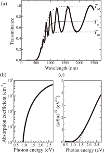
Fig. 1. (a) Transmission spectrum for sample A, where  . (b) Absorption spectrum. (c) (αdhν)1/2 versus hν plot.22)
Download figure:
Standard image High-resolution image3.2. Minority-carrier diffusion length
Figures 2(a) and 2(b) show the secondary electron (SE) and EBIC images of BaSi2 on Si(111), respectively, with Vac = 5 kV.24) To obtain Figs. 2(a) and 2(b), we used the same BaSi2 film as reported in Ref. 24, but we formed the Schottky contact with the Al wire at different positions to measure L. In the EBIC method, the carriers generated within the diffusion length of the n-type BaSi2 are collected by the electric field under the Schottky contact and sensed as a current in the external circuit. The brighter regions indicate a higher number of electron-beam-induced carriers collected in the BaSi2. Figure 2(c) shows the plot of EBIC line-scan data along the broken line AA' in Fig. 2(b). The EBIC profiles show a clear exponential dependence on the distance from the metal contacts. The contribution of carriers generated within the n-Si substrate to the measured EBIC signals can be excluded as described above. In this work, L was estimated to be approximately 8.6 µm for holes in the n-BaSi2 on Si(111), assuming that the EBIC profile varies as exp(−x/L). Here, x is the distance from the metal edge along the line, which is almost the same as that reported previously.24)
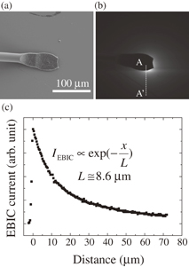
Fig. 2. (a) SE and (b) EBIC images around the Al contact. (c) Experimental EBIC line-scan profile along dotted line AA' in (b).25)
Download figure:
Standard image High-resolution image3.3. Minority-carrier lifetime
Figure 3 shows 12 × 12 µm2 EBSD crystal orientation maps and distribution histograms of the grain area fraction in samples A–H. The red, blue, and green colors indicate that three epitaxial variants of a-axis-oriented BaSi2 exist on Si(111).24) The average grain area of the BaSi2 varied in the range from 2.6 to 23.3 µm2.28) It seems reasonable to think that the density of BaSi2 GBs decreases when the average grain area increases. Figure 4(a) shows a typical example of the normalized µ-PCD decay curve, obtained for sample C. The decay curve can be divided into three decay modes, that is, Auger recombination and Shockley–Read–Hall (SRH) recombinations without and with the carrier-trapping effect, denoted by decay times of τAuger, τSRH, and τSRH-trapping, respectively. The inserted dotted lines correspond to the exponential decays of these three modes. In the SRH recombination, we assume a trap level in the band gap, where the recombination of electrons and holes occurs via this level.54) Basically, upon laser irradiation, Auger recombination occurs in the initial stage because of the high absorption coefficient of BaSi2 for the 349 nm light, and the high excitation in the µ-PCD measurement. The initial excess carrier concentration, Δn, at the surface reaches the range of 1018 to 1021 cm−3, which was calculated from the absorption coefficient of BaSi2 at a wavelength of 349 nm and the irradiated laser intensity. Thus, it is difficult to avoid Auger recombination in the present µ-PCD measurement. Since there is an electric field in BaSi2 due to the difference in electron affinity between BaSi2 (3.2 eV)55) and Si (4.0 eV), carrier separation occurs at the same time as Auger recombination, followed by SRH recombination. In this work, we used τSRH as a measure to investigate the minority-carrier properties of BaSi2 films. This is because the first decay mode, Auger recombination, is not likely to happen under AM 1.5 illumination. Thus, the second decay mode is very important; τSRH should be sufficiently large to achieve high efficiency. τSRH decreased with increasing Δn. This is because Δn is orders of magnitude higher than the majority-carrier (electron) density of approximately 1016 cm−3 at equilibrium in undoped n-BaSi2. Such a high carrier injection level leads to multicarrier recombination. We therefore adopted τSRH when Δn was about 1016 cm−3. For this small Δn, it was confirmed that the influence of the high-resistivity Si substrate on τSRH was negligible, as shown by experiments using exfoliated BaSi2 films.56)

Fig. 3. 12 × 12 µm2 EBSD crystal orientation maps of the BaSi2 epitaxial films and distribution histograms of BaSi2 grain area fraction in samples A–H. The average grain area for each sample is also presented.28)
Download figure:
Standard image High-resolution image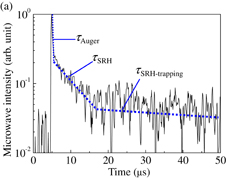
Download figure:
Standard image High-resolution image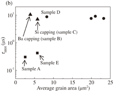
Fig. 4. (a) Normalized µ-PCD decay curve of sample C. (b) Dependence of τSRH on average grain area of BaSi2.28)
Download figure:
Standard image High-resolution imageFigure 4(b) shows the dependence of τSRH on the average grain area of BaSi2 for samples A–H. For the samples without capping layers, τSRH values were grouped into two, that is, approximately 0.4 µs (samples A and E) and 8–10 µs (samples D and F–H). In each group, τSRH is almost the same, regardless of the BaSi2 average grain area. The difference between the two groups was due to the surface conditions.28) BaSi2 films with a large τSRH had cloudy surfaces, whereas those with a smaller τSRH had mirror surfaces. However, the problem was that we were not able to intentionally grow BaSi2 films with a large τSRH. This problem was overcome by in situ capping with a 3 nm Ba or Si layer on BaSi2 in samples B and C, as shown in Fig. 4(b). X-ray photoemission spectroscopy analyses revealed that the O atoms may play an important role in making τSRH large.28) Currently, we are able to form BaSi2 films with a large τSRH of approximately 10 µs, regardless of the grain size of BaSi2, by capping the surface of BaSi2 with the Ba or Si layer. This means that τSRH is not influenced by GBs. This result is consistent with what we expect from the potential variations around the GBs,29) where the potentials are higher at GBs and thus minority carriers (holes) are not attracted towards the defective GBs.
3.4. Photoresponse spectra, photocurrent density, and open-circuit voltage
In this subsection, we attempt to deduce the expected photocurrent density in a BaSi2 homojunction diode. Analytical expressions for the photogenerated and dark current densities can be obtained only when the dopant concentration, minority-carrier lifetime, and other parameters are assumed constant.57,58) We assume here a simple p+n abrupt junction diode, as shown in Fig. 5. When monochromatic light of energy E is incident on the front surface (p+), the generation rate of electron–hole pairs per unit volume per unit time at a distance x from the semiconductor surface, G(x), is given by

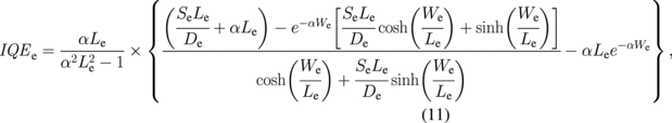
Here, Φ0 is the number of photons incident per unit time per unit area per unit bandwidth at energy E, and R is the reflectance at the surface. These three parameters vary with E, and thus G(x) depends on E. The total photocurrent density j is given by the sum of the current density due to electrons generated within the neutral p+-BaSi2 region, je, the current density due to electron–hole pairs generated within the depletion region, jDL, and the current density due to holes generated within the neutral n-BaSi2 region, jh. The internal quantum efficiency IQE is equal to

Once IQE is derived, the total photocurrent density  obtained from the solar spectral range is given by
To increase JL, we should minimize R and maximize IQE over the solar spectral range. Therefore, IQE is a measure of the quality of the diode. Assuming that the quantum efficiency is 100% because of the electric field within the depletion region, jDL is expressed as

Here, q is the elemental charge and W is the depletion region width.
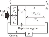
Fig. 5. Dimensions and parameters in a simple p+n abrupt homojunction diode.
Download figure:
Standard image High-resolution imageWe next derive je. The excess electron concentration  in the neutral p+-type layer (0 ≤ x ≤ We) is given by solving the current continuity equation for electrons as follows:
Here, De is the diffusivity and τe is the minority-carrier (electron) lifetime. There are two boundary conditions. At the surface, we have surface recombination with a recombination velocity Se under the condition of

where np and np0 are the electron concentrations in the neutral p+ layer under biased conditions and under thermal equilibrium, respectively. At the depletion edge, the electron concentration is given by
Here, V is the forward voltage applied across the p+n junction under illumination. Once np(x) is obtained, je is given by
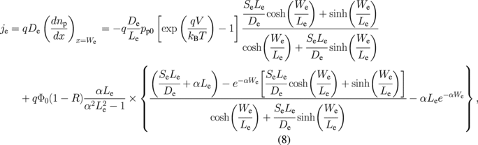
where Le = (Deτe)1/2 is the diffusion length of electrons in the neutral p+-type layer. The first term in Eq. (8) is the dark current flowing in the opposite direction to the photocurrent.
In the same way, jh is given by
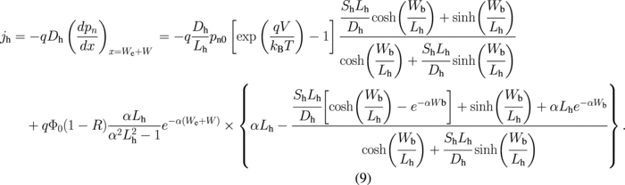
Here, Dh is the diffusivity and τh is the minority-carrier (hole) lifetime in the neutral n-type layer. The minority-carrier (hole) diffusion length Lh is expressed as (Dhτh)1/2. From Eqs. (4), (8), and (9), the contributions of jDL, je, and jh to IQE, that is, IQEDL, IQEe, and IQEh, respectively, are described as follows:


We next investigate the dependence of IQE on various parameters. For α, we used the experimental data shown in Fig. 1(b). As the diffusivity is not highly sensitive to impurities and defects,58) we set both De and Dh to be 0.1 cm2/s, because Lh and τh were approximately 10 µm in Fig. 2(c) and 10 µs in Fig. 4(b),24,25,27,28) respectively. When the impurity concentrations in the p+ and n layers, that is, NA and NV, are set to be 1018 and 1016 cm−3, respectively, W is estimated to be 0.4 µm and the built-in voltage is 1.0 V, assuming that the permittivity of BaSi2 is approximately 15.21,59) The effective densities of states at the conduction band and valence band, that is, NC and NV, are 2.6 × 10¹⁹ and 2.0 × 1019 cm−3, respectively, from the principal-axis components of the effective mass tensor for electrons and holes.21) The square of the intrinsic carrier concentration,  , is calculated to be 8 × 1016 cm−3 at RT. Other parameters are summarized in Table I. The complete ionization of impurity atoms is also assumed. Regarding surface recombination velocities, the BaSi2 layer thickness dependence of τh revealed that the surface recombination velocity is as low as approximately 8 cm/s in undoped n-BaSi2.27) Thus, we varied Se and Sh from 8 to 100 cm/s, as shown in Table I.
Table I. Parameters of BaSi2 homojunction diode.
| Sample | NA (cm−3) | We (µm) | Le (µm) | Se (cm/s) | W (µm) | ND (cm−3) | Wb (µm) | Lh (µm) | Sh (cm/s) |
|---|---|---|---|---|---|---|---|---|---|
| pn-A | 1018 | 0.1 | 0.1 | 8 | 0.4 | 1016 | 1.5 | 10 | 8 |
| pn-B | 1018 | 0.1 | 0.1 | 8 | 0.4 | 1016 | 2.5 | 10 | 8 |
| pn-C | 1018 | 0.05 | 0.1 | 8 | 0.4 | 1016 | 1.5 | 10 | 8 |
| pn-D | 1018 | 0.05 | 0.1 | 100 | 0.4 | 1016 | 1.5 | 10 | 8 |
| pn-E | 1018 | 0.05 | 0.1 | 8 | 0.4 | 1016 | 1.5 | 10 | 100 |
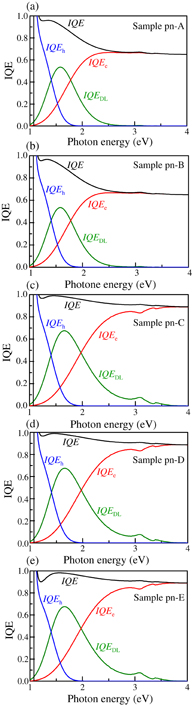
In Figs. 6(a) and 6(b), IQE is almost the same for samples pn-A and pn-B, although Wb increases from 1.5 µm in sample pn-A to 2.5 µm in sample pn-B. This means that Wb = 1.5 µm is sufficiently large. When We decreases from 0.1 to 0.05 µm, IQE increases particularly at higher energies in samples pn-C to pn-E. This is attributed to the enhancements of IQEe and IQEDL. Since the absorption coefficient of BaSi2 is very high, the contributions of the surface p+-layer and the depletion region to IQE become pronounced when We decreases. This result implies that we need to design We to be equal to Le or smaller. In samples pn-C to pn-E, there is no significant difference in IQE regardless of differences in Se and Sh. This means that IQE is not very sensitive to surface conditions in a BaSi2 homojunction solar cell.
Fig. 6. Calculated internal spectral responses for samples pn-A to pn-E. Individual contributions of IQEe, IQEDL, and IQEh to the total IQE are shown.
Download figure:
Standard image High-resolution image
We next discuss the expected conversion efficiency of the diodes. Considering that the hole concentration in the neutral n-type layer at thermal equilibrium, pn0, is much higher than np0 because of the p+n junction, the dark current density of the diode, Jdark, is dominant from the contribution of the n-type layer and is given by
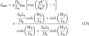
Thus, the reverse saturation current density Js is expressed as
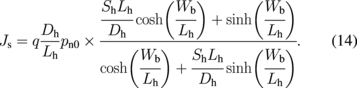
The values of Js and JL, and the expected open-circuit voltage VOC under AM 1.5 illumination for samples pn-A to pn-E are related by

The results are summarized in Table II. Assuming that the fillfactor is 0.8 regardless of VOC and R = 0, the conversion efficiency is calculated to be approximately 25% in samples pn-C and pn-D even though the total layer thickness is only 2 µm. It is true that we overestimated VOC and JL because R cannot be 0, and other residual effects such as series resistance and shunt resistance should be taken into consideration in actual devices. However, it is safe to conclude that BaSi2 is indeed an attractive material for thin-film solar cell applications.
Table II. Calculated Js, JL, and VOC for samples pn-A to pn-E, assuming R = 0 and FF = 0.8.
| Sample | JS (A/cm2) | JL (A/cm2) | VOC (V) | Pout (mW/cm2) |
|---|---|---|---|---|
| pn-A | 2.90 × 10⁻¹⁷ | 3.17 × 10⁻² | 0.897 | 22.7 |
| pn-B | 4.08 × 10⁻¹⁷ | 3.18 × 10⁻² | 0.888 | 22.6 |
| pn-C | 2.90 × 10⁻¹⁷ | 3.55 × 10⁻² | 0.900 | 25.6 |
| pn-D | 2.90 × 10⁻¹⁷ | 3.55 × 10⁻² | 0.900 | 25.6 |
| pn-E | 1.28 × 10⁻¹⁶ | 3.51 × 10⁻² | 0.861 | 24.2 |
4. Conclusions
We calculated the photoresponse spectra of BaSi2 p+n abrupt homojunction diodes using experimentally obtained absorption coefficients, the minority-carrier diffusion length, and the minority-carrier lifetime, and discussed the influences of parameters such as emitter and base layer thicknesses and surface recombination velocities. It was found that IQE is not very sensitive to Se, Sh, and Wb, whereas We significantly affects on IQE particularly in a high-energy region. This is because the absorption coefficient of BaSi2 is high. Thus, we need to carefully consider the relationship between We and Le in the emitter layer when we design We. A conversion efficiency of approximately 25% is expected for 2-µm-thick BaSi2 homojunction diodes under ideal conditions.
Acknowledgements
I thank Professor N. Usami and Dr. K. O. Hara of Naogya University, and Dr. T. Sekiguchi and Dr. K. Watanabe of the National Institute for Materials Science for their help, discussions and encouragement to pursue this work. I am also particularly grateful to Dr. K. Toko, Dr. W. Du, Dr. M. Ajmal Khan, and present and past students in my laboratory of the University of Tsukuba for their experiments and fruitful discussions. This work was financially supported in part by the Core Research for Evolutionary Science and Technology (CREST) of the Japan Science and Technology Agency (JST).