Abstract
CMOS utilizing high-mobility III–V/Ge channels on Si substrates is expected to be one of the promising devices for high-performance and low power advanced LSIs in the future, because of its enhanced carrier transport properties. However, there are many critical issues and difficult challenges for realizing III–V/Ge-based CMOS on the Si platform such as (1) the formation of high-crystal-quality Ge/III–V films on Si substrates, (2) gate stack technologies to realize superior MOS/MIS interface quality, (3) the formation of a source/drain (S/D) with low resistivity and low leakage current, (4) process integration to realize ultrashort channel devices, and (5) total CMOS integration including Si CMOS. In this paper, we review the recent progress in III–V/Ge MOS devices and process technologies as viable approaches to solve the above critical problems on the basis of our recent research activities. The technologies include MOS gate stack formation, high-quality channel formation, low-resistance S/D formation, and CMOS integration. For the Ge device technologies, we focus on the gate stack technology and Ge channel formation on Si. Also, for the III–V MOS device technologies, we mainly address the gate stack technology, III–V channel formation on Si, the metal S/D technology, and implementation of these technologies into short-channel III–V-OI MOSFETs on Si substrates. On the basis of the present status of the achievements, we finally discuss the possibility of various CMOS structures using III–V/Ge channels.
Export citation and abstract BibTeX RIS
1. Introduction
Since the introduction of the 90 nm technology node, a variety of technology boosters such as strained-Si and SiGe channels, high-k/metal-gate gate stacks, and ultrathin Si-on-insulator (SOI) and multi-gate structures have been introduced for the equivalent scaling of the device performance.1) However, stringent demands on low power consumption are one of the most critical issues for the 10 nm technology node and beyond. Here, the enhancement of the carrier transport properties of complementary metal–oxide–semiconductor (CMOS) channels is quite effective in obtaining high performance CMOS operation with low power supply voltage,1–3) which is mandatory for a reduction in power consumption. As a result, the high-mobility-channel CMOS on the Si platform is strongly expected to be one of the promising devices for high-performance and low-power logic large-scale integrated circuits (LSIs) in the future technology nodes.
To achieve a high current drive with a low power supply, the channel materials with high mobility and, more essentially, low effective mass, are preferable even in the ultrashort channel regime.3–8) The carrier transport in metal–oxide–semiconductor field-effect transistors (MOSFETs) with a channel length (Lch) of less than 100 nm can be regarded as quasi-ballistic transport, where a higher injection velocity and lower back scattering rate near the source edge are needed to increase the on-current (Ion).6–9) Here, a lower effective mass along the channel length direction can lead to a higher injection velocity, irrespective of thermal velocity or Fermi velocity.3,7) Also, a smaller back scattering rate and lower effective mass provide a higher mobility of channel materials. As a result, low-field mobility as a material parameter is still a good indicator for a high current drive under quasi-ballistic transport, while the effective mass is the essential parameter under full ballistic transport.
Table I shows the fundamental physical properties of the main semiconductor materials including Si, Ge, and III–V materials.10–15) The lightest hole effective mass and the highest hole mobility of Ge indicate that Ge is very suitable for p-MOSFET applications. Also, the comparatively high electron mobility and low electron effective mass of Ge also suggest that Ge is promising for CMOS applications.
Table I. Lists of electron and hole mobilities, electron and hole effective masses, and bandgap and permittivity for Si, Ge, and typical III–V compound semiconductors.
| Si | Ge | InP | GaAs | In0.47Ga0.53As | InAs | GaSb | InSb | |
|---|---|---|---|---|---|---|---|---|
| Electron mobility (cm2 V−1 s−1) | 1600 | 3900 | 5400 | 9200 | 14000 | 40000 | 5000 | 77000 |
| Electron effective mass (/m0) | mt/ml, 0.19/0.16 | mt/ml, 0.082/1.467 | 0.08 | 0.067 | 0.041 | 0.026 | 0.042 | 0.014 |
| Hole mobility (cm2 V−1 s−1) | 430 | 1900 | 200 | 400 | 300 | 500 | 850 | 850 |
| Hole effective mass (/m0) | mHH/mLH 0.53/0.16 | mHH/mLH 0.35/0.043 | mHH/mLH 0.55/0.083 | mHH/mLH 0.46/0.051 | mHH/mLH 0.36/0.026 | mHH/mLH 0.37/0.043 | mHH/mLH 0.38/0.014 | mHH/mLH 0.53/0.16 |
| Band gap (eV) | 1.12 | 0.66 | 1.34 | 1.42 | 0.75 | 0.36 | 0.72 | 0.14 |
| Permittivity | 11.8 | 16 | 12.4 | 13.2 | 13.9 | 14.6 | 15.7 | 17 |
As- and P-based III–V semiconductors such GaAs, InGaAs, InAs, and InP are suitable for n-MOSFET applications, because of their extremely high electron mobility and low electron effective mass, while those materials are not preferable for p-MOSFETs. In contrast, Sb-based III–V materials such as GaSb, InGaSb, and InSb are regarded as possible candidates for p-MOSFETs and CMOS, because of their higher hole mobility and lower hole effective mass.15) As a result, strong attention has recently been paid to CMOS utilizing high-mobility Ge/III–V channels on Si substrates as the future logic devices.
There are a variety of CMOS structures using III–V/Ge channels.16) The typical CMOS structures are schematically shown in Fig. 1. One of the ultimate CMOS structures is the co-integration of an As-based III–V n-MOSFET and a Ge p-MOSFET.2) In addition to the extremely high electron and hole mobilities, the quite low contact resistance with metals is also an important property from the viewpoint of logic CMOS applications. It is known that, because of the inherent strong surface pinning of these semiconductors with metals,17) low Schottky barrier height (SBH) for electrons is obtained for InGaAs and InAs,18) and low SBH for holes is obtained for Ge.19,20)
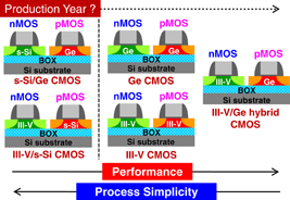
Fig. 1. Several CMOS structures using Ge/III–V channels.
Download figure:
Standard image High-resolution imageOn the other hand, Ge CMOS is also plausible in terms of the simplicity of the process/material integration, because the CMOS is composed of a single material. The key issue for Ge CMOS is the realization of high-performance Ge n-MOSFETs, which have not been fully obtained yet. Also, while III–V CMOS is another possible CMOS structure, there are still many choices of materials for CMOS, because III–V materials suitable for n-MOSFETs and p-MOSFETs are different in most cases, as shown in Table I. Also, the key issue in III–V CMOS is the realization of high-performance III–V p-MOSFETs, whose performance has not been sufficient yet either. Thus, CMOS structures for near-future applications could be integrated with strained-Si devices, although the performance improvement might be limited. As a result, realistic CMOS structures using high mobility materials are still strongly dependent on future progress in the device/process/integration technologies of III–V/Ge MOS devices, the amount of the performance enhancement and the yield/cost.
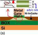
In addition, one of the most critical issues for CMOS under advanced technology nodes is the suppression of short-channel effects (SCEs), which must be satisfied by an ultrathin body (UTB) or nanowire channels with extremely-thin equivalent oxide thickness (EOT) gate stacks.1) Among a variety of UTB structures including FinFET, tri-gate devices, nanowire devices, planar UTB channel/ultrathin buried oxide (UTBOX)-based devices2,3,21,22) can be useful, because of their (1) simple device fabrication and easy integration with bulk MOSFETs, (2) further improvement of SCEs by combination with multi-gate structures, and (3) possibility of static and dynamic threshold voltage (Vth) control through UTBOX by back bias and/or substrate doping. Figure 2 shows possible device structures based on ultrathin body Ge/III–V channels on the Si platform. Here, gate stacks with high-k gate insulators and metal gates are mandatory for a thin EOT. Also, metal source/drain (S/D) structures are assumed here for suppressing the parasitic S/D resistance. In this study, the combination of high-mobility-channel MOSFETs with the planar UTB structure is emphasized.
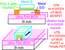
Fig. 2. Possible device structures based on ultrathin body Ge/III–V channels on the Si platform.
Download figure:
Standard image High-resolution imageThe critical technological issues and difficult challenges to realize high-mobility-channel CMOS on the Si platform are summarized23) as (1) the formation of high-crystal-quality Ge/III–V films on Si substrates, (2) gate stack technologies to realize superior MOS/MIS interface quality, (3) the formation of an S/D with low resistivity and low leakage current, (4) process integration to realize ultrashort channel devices, and (5) total CMOS integration including Si CMOS. In this paper, we present several possible and viable device technologies, which can solve these critical issues of CMOS using Ge and/or III–V channels with emphasis on a thin EOT and ultrathin body, which are mandatory for the future nodes.
The composition of this paper is as follows. First, a couple of Ge MOS device technologies are described in Sect. 2. One is the gate stack formation technology to realize a thin EOT and high carrier mobility, which is described in Sect. 2.1. In particular, high electron mobility is one of the strongest concerns in terms of Ge CMOS applications. The other technology is related to the thin body Ge formation on Si substrates, which is described in Sect. 2.2. Here, we emphasize the Ge condensation technique, which is known to realize ultrathin body Ge-on-insulator (GOI) structures with a combination of conventional CMOS process technologies.
Next, we present several device technologies for realizing III–V MOSFETs in Sect. 3. First, the gate stack formation technologies are given in Sect. 3.1. Next, the III–V channel formation technologies are described in Sect. 3.2 with emphasis on direct wafer bonding of III–V films on Si substrates to realize III–V channels on Si wafers with a large wafer size, which is indispensable in the implementation to the Si platform. Next, we describe the S/D formation technologies in Sect. 3.3. Here, we focus mainly on the metal S/D structures, which are suitable for low parasitic resistance in UTB films. In Sect. 3.4, the channel engineering for quantum well (QW) UTB III–V-on-insulator (III–V-OI) channels and the results of short-channel III–V tri-gate MOSFETs on Si substrates are described as an example of integration of the above device technologies for satisfying both the SCEs and the suppression of mobility reduction.
Next, we briefly summarize the III–V/Ge CMOS structure in Sect. 4. The present status and the critical issues on Ge CMOS, III–V CMOS, and III–V/Ge CMOS are concisely described in Sects. 4.1, 4.2, and 4.3, respectively. Finally, we summarize the content.
2. Ge MOS device technologies
2.1. Ge gate stack technology
One of the most critical issues in Ge MOSFETs is the realization of gates stacks with superior MOS interfaces. In particularly, to obtain high electron mobility in Ge n-MOSFETs, careful MOS interface design and superior MOS interface properties are indispensable. Many recent studies24–48) have revealed that Ge oxide interfacial layers (IL) can provide superior MOS interfaces with lower Dit among the various Ge MOS interfaces. The typical energy distribution of Dit in Ge oxide/Ge interfaces has a symmetrical U-shape distribution,30,35–37,40,42,46) meaning that a sufficiently-low Dit is obtained even near the conduction band edge, which is quite important for high electron mobility. However, the realization of an ultrathin EOT while maintaining this low Dit is still challenging for Ge gate stacks with the Ge oxide ILs. This is because Ge oxides are chemically and physically unstable, and thin Ge oxides are easily degraded by exposure to air and any chemical solutions including water.29,34,49–51) Also, ultrathin Ge oxide formation is not very controllable, because Ge surfaces are easily oxidized at low temperature.50)
Recently, several methods to form gate stacks including the Ge oxide ILs have been developed to realize a low Dit and thin EOT at the same time.16,52–73) We have proposed a novel IL formation process employing electron-cyclotron resonance (ECR) oxygen plasma to form GeOx ILs after thin Al2O3 ALD.16,52–56) Also, we have demonstrated a revised version of gate insulator formation using ALD HfO2/Al2O3 stacks for further reducing EOT.16,57,60) The basic process flow is shown in Fig. 3. The key process in this gate stack formation is to form Ge oxides between Ge and Al2O3 after the deposition of thin high-k films including Al2O3 by exposing oxygen plasma with low plasma damage. The main advantages of this fabrication method for Ge gate stacks with Ge oxide ILs are summarized as follows: (1) The Al2O3 layer serves as a sufficient oxygen barrier, which suppresses the growth of unnecessarily-thick Ge oxide ILs, thanks to its intrinsic oxygen permeability. (2) The Al2O3 layer effectively prevents Ge surfaces from the direct exposure to ECR oxygen plasma and any damage during the fabrication processes, leading presumably to the reduction in the plasma and process damage to the MOS interfaces. (3) The low processing temperature in the ECR plasma oxidation, typically 300 °C or less,69) is expected to sufficiently suppress any thermal degradation of the Ge oxide/Ge interface.
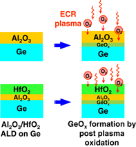
Fig. 3. Proposed Al2O3/GeOx/Ge and HfO2/Al2O3/GeOx/Ge gate stack formation process by oxidation using ECR oxygen plasma through a thin Al2O3 and a thin HfO2/Al2O3 layer, respectively, by ALD.
Download figure:
Standard image High-resolution imageWe have confirmed through X-ray photoelectron spectroscopy (XPS) analyses52,54,57,60) that the MOS gate stacks fabricated by oxidizing Al2O3/Ge and HfO2/Al2O3/Ge layers are basically composed of Al2O3/GeOx/Ge and HfO2/Al2O3/GeOx/Ge structures, respectively, though we are not able to fully exclude the possibility of slight intermixing of Ge, Al, and Hf at both interfaces in terms of the accuracy of the analyses. It should be noted that the application of post plasma oxidation to ALD HfO2/Ge interfaces leads to the HfGeOx formation through the intermixing of HfO2 and Ge oxides,57,60) which causes a high leakage current and high Dit of the fabricated Ge MOS structures. Thus, the insertion of the thin Al2O3 layer and the resulting HfO2/Al2O3 layered structure are needed to suppress this intermixing. The XPS analyses have also revealed that Ge oxides are not GeO2 but Ge sub-oxides, and that the averaged Ge oxide states determined by the chemical shift in the peak of the Ge 3d spectra change from GeO to GeO2 with increasing the Ge oxide IL thickness.52,54,56,61) Thus, the Ge oxide ILs are denoted as GeOx in this paper.
Figure 4 shows the relationship between Dit and EOT for the Al2O3-based and HfO2/Al2O3-based gate stacks with and without the post plasma oxidation.16,55,56,60,61,72) Here, EOT for Al2O3/GeOx/Ge was varied by changing the GeOx IL thickness under different plasma powers (300, 500, and 650 W) and different Al2O3 thicknesses from 1 to 1.5 nm at a given post plasma oxidation time of 10 s. Here, the data of Al2O3/GeOx/(100), (110), and (111) Ge MOS interfaces are shown. A thinner GeOx IL can be realized by lowering the plasma power as well as increasing the Al2O3 thickness. Post-deposition annealing (PDA) was carried out at 400 °C for 30 min in N2 for the capacitors. The Dit values obey the almost universal relationship against the GeOx thickness and resulting EOT, irrespective of the Ge surface orientations, indicating that Dit is determined by the thickness of GeOx IL and that Dit can be effectively reduced by introducing GeOx ILs. GeOx with ∼0.3 nm EOT (physical thickness of ∼0.5 nm) is needed to sufficiently reduce Dit. While the Al2O3/GeOx/Ge gate stacks can provide a Dit of as low as 1011 cm−2 eV−1 order, the low permittivity of Al2O3 poses a limitation on thinning EOT of approximately 1 nm, necessitating HfO2 for further scaling EOT.
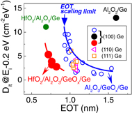
Fig. 4. Dit at Ei − 0.2 eV as a function of EOT of HfO2/Al2O3/(100) Ge and Al2O3/(100) Ge MOS interfaces with and without GeOx formed by ECR post plasma oxidation. EOT was varied by changing plasma oxidation conditions and the resulting thickness of GeOx ILs. Here, the data of Al2O3/GeOx/(110) and (111) Ge MOS are also shown.
Download figure:
Standard image High-resolution imageAs described above, the plasma oxidation of HfO2/Ge direct stacks provides inferior MOS interface properties with a high Dit and a high leakage current, because of the intermixing of HfO2 and GeOx during the oxidation. Thus, ultrathin Al2O3 films were inserted between HfO2 and Ge as an interdiffusion control layer. The EOT of the Au/HfO2 (2.2 nm)/Al2O3 (0.2 nm)/GeOx/p-Ge MOS capacitors was changed by using different post plasma oxidation times of 0, 5, 10, 15, and 25 s. PDA was also carried out at 400 °C for 30 min in N2. The values of Dit as a function of EOT are also plotted in Fig. 4. While a similar decreasing trend of Dit with an increase in EOT as that in the Al2O3/GeOx/Ge MOS structure is observed, the relationship between EOT and Dit in the HfO2/Al2O3/GeOx/Ge MOS structure is shifted toward thinner EOT direction because of the higher permittivity of HfO2.
Figure 5(a) shows a transmission electron microscopy (TEM) photograph of a fabricated HfO2/Al2O3/GeOx/Ge gate stack with an EOT of 0.76 nm, after post plasma oxidation using 500 W plasma for 15 s. The TEM image shows a clear boundary of the interface between HfO2 and Al2O3, while the interface between Al2O3 and GeOx is not visible because of the small difference in the density between both layers. As a result, we can consider this gate stack as the 2.2-nm-thick HfO2 and ∼0.55-nm-thick IL composed of the 0.2-nm-thick Al2O3 and the 0.35-nm-thick GeOx. Figures 5(b) and 5(c) show the frequency dispersion and the measurement temperature dependence of the capacitance–voltage (C–V) characteristics of the HfO2 (2.2 nm)/Al2O3 (0.2 nm)/GeOx (0.35 nm)/Ge structure. The good C–V characteristics with small frequency dispersion measured at room temperature (RT) and no change in the minimum and maximum capacitances at different temperatures indicate the sufficient passivation of the Ge MOS interfaces. However, the hysteresis of the C–V curves with a sweep scan between 1 and −1.5 V amounts to ∼150 mV, which is attributable to slow traps in both IL and the HfO2 layer. Further reduction in slow traps and improvement of the long-term instability are present critical issues of the gate stacks using GeOx ILs.74,75) Figure 6 shows the drain current–gate voltage (Id–Vg) characteristics of n- and p-MOSFETs with the HfO2 (2.2 nm)/Al2O3 (0.2 nm)/GeOx (0.35 nm)/Ge gate stacks under an EOT of 0.76 nm. The normal operation of n- and p-MOS devices can be confirmed from the Id–Vg characteristics. These Ge p- and n-MOSFETs show the on/off current ratios of ∼104 and ∼103, and the S factors of 85 and 80 mV/dec, respectively.

Fig. 5. (a) Frequency dispersion and (b) measurement temperature dependence of C–V characteristics of an HfO2 (2.2 nm)/Al2O3 (0.2 nm)/GeOx (0.35 nm)/Ge structure after post plasma oxidation using 500 W plasma for 15 s, and (c) cross-sectional TEM image of this MOS interface.
Download figure:
Standard image High-resolution image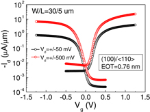
Fig. 6. Id–Vg characteristics of the Ge p- and n-MOSFETs with HfO2 (2.2 nm)/Al2O3 (0.2 nm)/GeOx (0.35 nm)/Ge gate stacks.
Download figure:
Standard image High-resolution imageThe hole and electron mobilities of the Ge p- and n-MOSFETs with the 0.76-nm-EOT HfO2 (2.2 nm)/Al2O3 (0.2 nm)/GeOx (0.35 nm)/Ge gate stacks are plotted in Figs. 7(a) and 7(b), respectively. In comparison, the mobilities of the Ge MOSFETs with HfO2/Al2O3/Ge, HfO2/Ge, and 20-nm-thick thermal oxidation GeO2/Ge gate stacks are also shown here. In addition, the Si universal mobility76) for electrons and holes is shown. It is found that the HfO2/Al2O3/GeOx/Ge gate stacks provide much higher electron mobility than the HfO2/Al2O3/Ge and HfO2/Ge direct interfaces. The hole mobility of p-MOSFETs with the HfO2/Al2O3/GeOx/Ge gate stacks is even higher than the Si universal hole mobility and the mobility with the thick GeO2/Ge stack. Also, the electron mobility of n-MOSFETs with the HfO2/Al2O3/GeOx/Ge gate stacks in the high-Ns region is comparable to or higher than the Si universal electron mobility and the mobility with the thick GeOx. These results indicate that the existence of GeO2 interfaces with a low Dit is essential to achieve higher electron and hole mobilities of Ge MOSFETs. These high electron and hole mobilities even in this ultrathin EOT range demonstrate that HfO2/Al2O3/GeOx/Ge gate stacks can realize high-performance Ge n- and p-MOSFETs with minimal mobility expense under aggressive scaling of EOT.

Download figure:
Standard image High-resolution image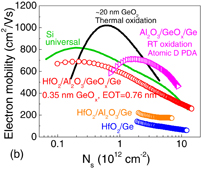
Fig. 7. (a) Electron mobility of the Ge n-MOSFETs and (b) hole mobility of the Ge p-MOSFETs with the HfO2 (2.2 nm)/Al2O3 (0.2 nm)/GeOx (0.35 nm)/Ge gate stacks, compared with those of the Ge MOSFETs with HfO2/Al2O3/Ge, HfO2/Ge, and 20-nm-thick GeO2/Ge gate stacks (solid black line). The Si-universal mobilities are shown by the solid green line. In addition, the effective electron mobility of the Al2O3/GeOx/Ge stack with PDA using atomic deuterium (D) is also shown in (a).
Download figure:
Standard image High-resolution imageOn the other hand, the mobility reduction of Ge MOSFETs, particularly in the high-Ns region, is still a critical issue of Ge CMOS, because MOSFETs usually operate in this high Ns region. To further improve the effective mobility in the high Ns region, we have introduced two mobility enhancement technologies. One is the suppression of MOS interface roughness by post plasma oxidation at RT.59,69,71,77) The oxidation temperature dependence of the GeOx/Ge interface roughness was directly examined by TEM. Figure 8 shows cross-sectional TEM images of the Al2O3/GeOx/Ge structures fabricated at the plasma oxidation temperature of 300 °C and RT. Larger roughness is observed at the GeOx/Ge interface grown at 300 °C, while a reduction of the GeOx/Ge interface roughness is observed for the one grown at RT. Figure 8 also shows the effective hole and electron mobilities in the Ge p- and n-MOSFETs with 300 °C and RT post plasma oxidation. It is found that the effective mobility of Ge p- and n-MOSFETs with RT oxidation is higher by 20 and 25%, respectively, at an Ns of 1013 cm−2, than those with 300 °C oxidation, which is attributable to the reduction of GeOx/Ge interface roughness by RT post plasma oxidation. In comparison, the hole mobilities with RT oxidation are also plotted in Fig. 7(a), confirming that the highest mobility is obtained in the high-Ns region for this interface.

Fig. 8. Cross-sectional TEM images of the GeOx/Ge interfaces formed by 300 °C and RT post plasma oxidation and the comparison of effective mobility in Ge MOSFETs with 300 °C and RT oxidized GeOx (1.2 nm)/Ge interfaces for both holes and electrons.
Download figure:
Standard image High-resolution imageThe other mobility enhancement technology is the reduction in the trapping effect of carriers into Dit inside the conduction and valence bands by atomic deuterium (D) annealing.62) We have revealed through Hall mobility measurements that the effective mobility is degraded by a large amount of Dit inside the conduction and valence bands.59,71) In addition, we have found that this Dit inside the conduction band can be reduced by PDA in atomic deuterium (D) atmosphere at 400 °C.62) The electron effective mobility after the atomic D PDA is also shown in Fig. 7(b). The mobility enhancement in the high-Ns region is clearly observed. We have confirmed that the Hall mobility does not change for n-MOSFETs with and without the atomic D PDA. Thus, this increase in the mobility with PDA is attributed to the reduction in Dit inside the conduction band, which decreases the amount of trapping of inversion-layer electrons resulting in the increase of Ns at a given Vg value.
2.2. Ge channel formation on Si
High-crystal-quality Ge channel formation on Si substrates as well as the mobility enhancement due to strain are indispensable in realizing III–V/Ge or Ge CMOS on the Si platform.78) It should be noted here that Ge channels thinner than 20 or 10 nm are strongly needed in advanced logic devices, irrespective of planar structure such as fully-depleted SOI or vertical Fin structures, to realize high immunity against the short-channel effects, which is one of the most difficult challenges in scaled MOSFETs. There are many ways78,79) to form Ge layers on Si or GOI structures, such as selective epitaxy of Ge films on Si,80,81) smart-cut GOI wafers,82–84) direct wafer bonding,79,85–89) Ge condensation,89–92) the lateral overgrowth of Ge films on insulators,93,94) and direct epitaxy of Ge films on crystal oxides.95,96) Among them, ultrathin body GOI structures formed by the Ge condensation technique89–92) are promising for the advanced CMOS logic devices. Figure 9(a) shows the schematic process flow of the Ge condensation technique, where SiGe films epitaxially grown on SOI substrates are thermally oxidized. Then, because of the stability of SiO2 against GeO2, only SiO2 is formed, Ge atoms are segregated at the SiO2/SiGe interface and diffused toward the deeper region.97,98) When all Si atoms included in the initial SOI and the SiGe epitaxial layer are oxidized, a pure GOI layer can be formed. The advantages of the Ge condensation technique are listed as follows: (1) A GOI thinner than 20 or 10 nm can be formed, (2) only conventional processes such as oxidation and SiGe epitaxial growth are employed, and (3) selective condensation for patterned substrates is suitable for the CMOS integration.3,99,100) Figure 9(b) shows an example of a CMOS structure composed of strained-SOI n-MOSFETs and Ge/SiGe p-MOSFETs formed by local Ge condensation of SiGe/strained-SOI layers, where epitaxial growth of the SiGe films and the Ge condensation are performed only in the p-MOSFET areas.
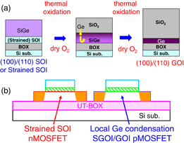
Fig. 9. (a) Concept of GOI channel formation by Ge condensation technique. (b) Schematic cross section of a CMOS structure composed of strained-SOI n-MOSFETs and Ge/SiGe p-MOSFETs formed by local Ge condensation of SiGe/strained-SOI layers.
Download figure:
Standard image High-resolution imageOn the other hand, one of the most critical problems of GOI formed by the Ge condensation technique is the defect formation associated with the stress relaxation during the condensation process90,101,102) and the resulting residual high hole concentration in GOI layers.103–105) The black symbols in Fig. 10 show the compressive strain during Ge condensation evaluated by Raman spectroscopy for SGOI layers on SOI substrates. Because of the difference in the lattice constant between Si and Ge and the strong bonding between initial SOI substrates and SiO2 buried oxides, the increase in the Ge content of the SGOI leads to an increase in the compressive strain. However, when the amount of strain is very high, the strain cannot be sustained in the SGOI layer and starts to be relaxed by generating dislocations through the SGOI layer. The dashed line indicates the compressive strain of the pseudo-morphic SiGe layer. Thus, the deviation from this line indicates the strain relaxation. Almost full relaxation in the SGOI with a higher Ge content suggests the generation of a high density of dislocations and defects in SGOI. We have optimized the oxidation process condition during the condensation process, where a higher oxidation temperature and intermixing annealing are employed, leading to a residual hole concentration of 1017 cm−3 or less.106) However, sufficient elimination of defects in the SGOI has not been realized yet.
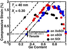
Fig. 10. Compressive strain during Ge condensation evaluated by Raman spectroscopy for SGOI layers on XsSOI with 1.14% tensile strain (blue circle), sSOI with 0.8% tensile strain (red circle), and SOI with no strain (black circle). The dashed line and the dotted line indicate that layers are pseudomorphic on each substrate. Deviation from the lines indicates strain relaxation.
Download figure:
Standard image High-resolution imageA possible solution for this problem can be the utilization of high-Ge-content SGOI channels with less strain relaxation by any technology to reduce the dislocation and defect densities. Here, one way to suppress the strain relaxation of the SGOI is to employ SOI substrates with tensile strain as starting materials.107,108) This is because the SOI substrates with tensile strain has smaller lattice mismatch with SiGe, resulting in the reduced strain in the SGOI. As a result, more highly-strained SGOI channels can be realized at a given Ge content. Figure 10 also shows the strain relaxation properties of the SGOI layers during the Ge condensation process on two types of strained-SOI substrates, an sSOI substrate with 0.8% tensile strain (red symbols) and an XsSOI substrate with 1.14% tensile strain (blue symbols). The parallel shift toward the higher Ge content of the compressive strain is simply explained by the change in the lattice constant of Si due to strain. It is found that the higher tensile strain in the initial SOI substrate provides a higher peak compressive strain. As a result, using SOI with tensile strain as the initial substrate can realize a higher compressive strain in a higher Ge content, which can significantly contribute to the enhancement of hole mobility.
Figures 11(a) and 11(b) show the effective hole mobility of SGOI p-MOSFETs with Ge contents of 58 and 87–93%, respectively, on SOI, sSOI, and XsSOI as a function of Ns. The hole mobilities of Si MOSFETs are also shown for comparison.76) The SGOI p-MOSFETs are operated under the back gate configuration. It is found that SGOI p-MOSFETs fabricated on the strained-SOI substrates yield a higher hole mobility than those on unstrained SOI. Figure 11(c) shows the enhancement factor of the hole mobility of SGOI p-MOSFETs against the Si hole mobility as a function of Ns. We have found that a quite high hole mobility enhancement factor of ∼8 against the hole mobility in Si p-MOSFETs is obtained for SGOI p-MOSFETs with a Ge content of 0.9, fabricated on strained-SOI substrates with bi-axial tensile strain. We have confirmed that this mobility enhancement can be quantitatively represented by the combined effects of the Ge content and the compressive strain,108) indicating that the quite high hole mobility on the strained-SOI substrates is attributed to higher compressive strain in the high Ge content region. As a result, local Ge condensation applied to p-MOSFET regions can provide realistic and effective CMOS integration on a strained-SOI platform, as shown in Fig. 9(b), because high hole mobility in SGOI p-MOSFETs can be combined with high electron mobility in strained-SOI n-MOSFETs.
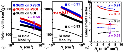
Fig. 11. Effective hole mobility of SGOI p-MOSFETs with Ge contents of (a) 58% and (b) 87–93% on XsSOI, sSOI, and SOI with Si hole mobility (Ref. 15) as a function of Ns. (c) Enhancement factor of hole mobility of SGOI p-MOSFETs against Si hole mobility as a function of Ns.
Download figure:
Standard image High-resolution image3. III–V MOS device technologies
3.1. III–V gate stack technology
The MOS interface control and EOT scaling are more problematic for III–V semiconductors than for Ge, because it is well known through the long history of intensive studies that III–V MOS interfaces have a high density of interface states and interface defects.15,109–112) Thus, III–V gate stack technologies for high-quality MOS interfaces are quite important. Actually, one of the most important recent findings in the III–V MOS interface control has been the effectiveness of ALD Al2O3 films as a gate insulator for III–V materials such as GaAs and InGaAs in terms of the reduction in Dit,113–121) often attributed to the cleaning effect of trimethylaluminum (TMA) on the III–V surfaces.113–117) Figure 12(a) shows the experimental energy distributions of Dit as a function of surface potential for ALD Al2O3/InGaAs and ALD HfO2/InGaAs MOS capacitors at the deposition temperature of 250 °C.120) It is found that the ALD Al2O3/InGaAs interfaces exhibit a Dit of approximately (2–3) × 1012 cm−2 eV−1, which is a fairly good value for III–V MOS interfaces, while the ALD HfO2/InGaAs MOS interfaces exhibit a Dit of approximately 1014 cm−2 eV−1 order under the present deposition conditions. As a result, many groups have reported the high performance of InGaAs MOSFETs with ALD Al2O3 gate insulators.117–119,122–125) However, one of the drawbacks of Al2O3 as an gate insulator is the low dielectric constant (∼9), which is not sufficient to provide low EOT gate stacks with a low gate leakage current.
Download figure:
Standard image High-resolution image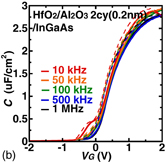
Fig. 12. (a) Energy distribution of Dit as a function of surface potential for ALD HfO2/InGaAs and ALD HfO2/Al2O3/InGaAs with different Al2O3 thicknesses. (b) C–V characteristics of a HfO2 (2 nm)/Al2O3 (0.2 nm)/InGaAs MOS capacitor with a CET of 1.08 nm.
Download figure:
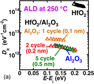
Standard image High-resolution imageOn the other hand, since HfO2 can be regarded as a promising gate insulator because of its high dielectric constant (∼22), the double layer HfO2/Al2O3/InGaAs gate stacks formed by inserting a thin ALD Al2O3 layer between HfO2 and InGaAs are promising,120,126–129) similar to the Ge gate stacks described in Sect. 2.1. To examine the impact of the Al2O3 interlayer thickness on the HfO2/Al2O3/InGaAs interface properties, we evaluated the MOS interface properties of the ALD HfO2/Al2O3/InGaAs MOS capacitors with changing Al2O3 thickness.119) Al2O3 and HfO2 layers were successively deposited at 250 °C by ALD. The ALD cycle number of Al2O3 was 1, 2, or 5 cycles, which corresponds to 0.1, 0.2, and 0.6 nm, and that of HfO2 was 100 cycles, corresponding to 10 nm. Au and Al were used as gate electrodes and the back contact, respectively. Post metallization annealing (PMA) was carried out at 400 °C for 1 min in N2 ambient.
Figure 12(a) also shows the energy distributions of Dit as a function of surface potential for the HfO2/Al2O3/InGaAs MOS capacitors. By inserting only the 2 cycle Al2O3 interlayer, Dit at the HfO2/InGaAs MOS interfaces drastically reduces from 2 × 10¹⁴ to 2 × 1012 cm−2 eV−1, which is the same as that at the thick Al2O3/InGaAs interfaces, indicating that the ultrathin 2 cycle Al2O3 interlayer effectively passivates the interface defects at the HfO2/InGaAs interfaces. Note that the 2 cycle Al2O3 layer (0.2 nm), less than one monolayer, can passivate 58% of an InGaAs surface, because the monolayer Al2O3 thickness is 0.38 nm.130) This result agrees with the theoretical prediction131–133) that, when a trivalent oxide like Al2O3 covers 50% or more of GaAs surface bonds, the HfO2/GaAs interface can be effectively passivated.
Figure 12(b) shows the C–V characteristics of a Au/HfO2 (2 nm)/Al2O3 (2 cycles: 0.2 nm)/InGaAs MOS capacitor. The accumulation capacitance of 2.9 µF/cm2 is realized at a Vg of 2.0 V, corresponding to a capacitance equivalent thickness (CET) of 1.08 nm, evaluated from the C–V curve fitting. The gate current density of the InGaAs gate stack with a CET of 1.08 nm was estimated to be 2.4 × 10² A/cm2 at Vg of (1 V + VFB), which is comparable to that of HfO2/Si gate stacks.134)
On the other hand, our recent works135–137) have also revealed that the Al2O3/InGaAs interface properties would still include a large amount of Dit inside the conduction band of InGaAs, which has been characterized by the difference in the Hall and effective mobilities. This Dit inside the conduction band can significantly degrade the effective mobility particularly in the high-Ns region. Also, a recent study has revealed that La2O3/InGaAs MOS interfaces can provide a lower Dit than Al2O3/InGaAs.138) Therefore, to further reduce the density of MOS interface defects of III–V MOS interfaces and improve the effective mobility of III–V MOSFETs, understanding of the physical origins of MOS interface defects and refinement of the gate stack technologies are still strongly needed.
3.2. III–V channel formation on Si
We consider that the high-quality III–V channel formation on Si substrates is one of the most difficult challenges in III–V MOSFET technologies on the Si platform. Actually, the high-quality and thin III–V channel formation on Si substrates seems to be much more difficult than Ge. The essential reasons for the difficulties in the III–V material formation on Si are (1) the lattice mismatch of typical III–V channel materials such as InGaAs and GaSb is much larger than Ge, (2) growth of polar semiconductors like III–Vs on non-polar semiconductors like Si tends to generate inherent defects like antiphase domains, and (3) group IV semiconductors like Si and Ge act as shallow impurities in III–Vs.
There can be two possible ways to form thin III–Vs on Si. One is the direct growth of III–V materials on Si substrates, similar to Ge. Here, graded buffer layers between Si and III–V channels are needed to accommodate the large lattice mismatch. Many efforts to reduce the buffer layer thickness have been made for the wafer level direct growth of III–V materials on Si substrates.139–143) The buffer layer thickness of 1 µm order seems to be needed to obtain high-quality III–V channel layers.140) While high-quality III–V channels with moderate dislocation density have been realized on Si substrates by this method, excessively thick graded buffers and the high wafer cost could cause difficulty in the realistic integration of III–V MOSFETs with Si CMOS.
Another promising approach using direct growth is the micro selective growth of III–Vs on Si,129,144–151) often called the aspect ratio trapping (ART) process. The advantages of the micro selective growth on III–V channels on the Si platform are (1) easy process integration into standard Si CMOS processes on large Si wafers, (2) easy integration of III–V and Si CMOS, and (3) reduction in dislocation density by termination of dislocations at the interfaces with shallow trench isolation. The development and significant progress of the ART process and the demonstration of InGaAs FinFETs on Si substrates, fabricated by this approach, have already been reported.129,151) While this approach is quite important from the viewpoint of compatibility with standard CMOS processes, there are still many issues to be solved, including the crystal quality of III–V channels and buffers, and the interface properties between Si and III–V are still problematic.
On the other hand, the other way to form thin III–Vs on Si is by wafer bonding of III–V channels with Si substrates,152–183) which is a good contrast to the direct growth. The advantages of the wafer bonding technique are (1) much better III–V material quality than the selective growth because of the optimized III–V growth condition and (2) easy formation of ultrathin III–V-OI structures, necessary for future technology nodes. Thus, the direct wafer bonding (DWB) process has been developed for forming ultrathin body III–V-OI structures on Si, such as InGaAs-OI,152–167,169,172–176,179,184) InAs-OI,165) InGaAs/InAs/InGaAs-OI,171,178) GaSb-OI,177,181,182) InGaSb-OI,168,170) and InAs/GaSb/InAs-OI181) and the operation of MOSFETs have been demonstrated on these III–V-OI structures.
Figure 13(a) shows schematic process flows of InGaAs-OI wafers formed by our developed DWB techniques using InGaAs channel layers grown on InP donor wafers.159,162,164,176) Here, multiple InP/InGaAs layers are inserted as etching sacrifice layers (ESLs) between the InP substrate and the top InGaAs channel layer to form an ultrathin InGaAs layer on Si with excellent uniformity. After pretreatment of InGaAs surfaces using NH4OH and (NH4)2Sx solutions, Al2O3 layers were deposited on both wafers by ALD. Then, the wafers were manually bonded in air, followed by post-bonding annealing. The InP substrates were removed by highly selective wet-etching with an HCl solution. The ELSs were etched with H3PO4:H2O2:H2O and HCl solutions. The high etching selectivity and ELSs allow us to fabricate extremely-thin body (ETB) III–V-OI on Si wafers. In addition, we can also precisely control the thickness of the BOX layers, because the BOX layers are the bonded Al2O3 layers formed by ALD. As a result, we can realize the ETB III–V-OI channel with the Al2O3 UTBOX layer,155,161) which is one of the most effective device structures for scaled MOSFETs, because of the strong immunity against short-channel effects and the threshold voltage controllability in a static or dynamic way by impurity doping beneath the BOX layer and back gate bias.
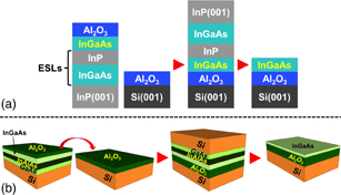
Fig. 13. Schematic process flows of InGaAs-OI wafers developed by direct wafer bonding (DWB) techniques using (a) an InP donor wafer and (b) a Si donor wafer. In process (a), multiple InP/InGaAs layers are inserted as etching sacrifice layers (ESLs) between the InP substrate and the top InGaAs channel layer to form an ultrathin InGaAs layer on Si. In process (b), InGaAs/InxAl−xAs/GaAs layers are epitaxially grown on Si substrates. After Al2O3 deposition as a BOX layer, CMP is carried out for surface smoothing for the Al2O3/III–V/Si wafer and the wafers are bonded to each other. Subsequent wet etching thins the top Si and the III–V buffer layers, resulting in the formation of InGaAs-OI on Si substrates.
Download figure:
Standard image High-resolution imageFigure 14 shows a TEM micrograph of the bonded interface.155,161) The 3.2-nm-thick InGaAs-OI layer shows excellent uniformity in thickness and smooth and abrupt interfaces. The thickness of the UTBOX layer was approximately 7.7 nm. We could not find any serious damage in the ETB InGaAs-OI layers, indicating that the developed DWB process is suitable for fabricating high-quality ETB III–V-OI on Si wafers. We have confirmed the high peak electron mobility of ∼3000 and ∼2000 cm2 V−1 s−1 for n- and p-InGaAs-OI front-gate MOSFETs, respectively, with a 100-nm-thick InGaAs-OI channel and an 11-nm-thick Al2O3 BOX.158) Also, 3.5-nm-thick ETB InGaAs-OI MOSFETs under the double-gate operation exhibited the Ion/Ioff ratio and S factor of ∼107 and 150 mV/dec, respectively, with an Ioff of as low as 0.1 pA/µm.155,161)
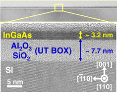
Fig. 14. Cross-sectional TEM micrograph of 3.2-nm-thick ETB InGaAs-OI on Si wafer with a 7.7-nm-thick UTBOX layer. The 3.2-nm-thick InGaAs-OI layer shows excellent uniformity and smooth and abrupt interfaces.
Download figure:
Standard image High-resolution imageOn the other hand, a clear drawback of the DWB technique using InGaAs channels on InP donor wafers is scalability in the wafer size of III–V-OI on Si substrates, because the size of InP donor wafers is much smaller than the 300-mm-Si wafers. To overcome this drawback of the DWB technique and to extend the wafer size of III–V-OI to 300 mm or larger, we have proposed and demonstrated the transfer of InGaAs grown directly on donor Si wafers to Si supporting substrates.183,185) The schematic process flow using the InGaAs channel layers grown on Si donor wafers is shown in Fig. 13(b). As an initial wafer, an InGaAs/InxAl−xAs/GaAs layer is epitaxially grown on a Si substrate. After Al2O3 deposition as a BOX layer, chemical mechanical polishing (CMP) is carried out for surface smoothing for the Al2O3/III–V/Si wafer and the wafers are bonded to each other. Here, ALD HfO2 is deposited on both the Al2O3/III–V/Si wafer and the Al2O3/Si supporting wafer to suppress any damage of the BOX layer during etching of the top Si substrate by HF. Subsequent wet etching thins the top Si and the III–V buffer layers, resulting in the formation of InGaAs-OI on Si substrates. Since III–V layers are grown on Si wafers, the present technique allows us to provide III–V-OI substrates with the same large wafer size as Si.
We have demonstrated InGaAs-OI MOSFETs on Si by using the InGaAs channels grown on 4-in. Si donor wafers as a preliminary work.183,185) We have confirmed that the Raman and PL spectra show high film quality of the bonded InGaAs-OI films on Si wafers. The fabricated n-MOSFETs have shown the high electron mobility of 1700 cm2 V−1 s−1 and the high enhancement factor of 3 against Si MOSFETs, which are almost the same as those of the n-MOSFETs fabricated by InGaAs on InP donor wafers. In addition, the fabricated MOSFETs exhibit a low drain leakage current and tight distribution of the leakage current, which are also almost the same as those of the MOSFETs fabricated by InGaAs on InP donor wafers. These results indicate the high quality of the InGaAs layers on Si with low defect density and the damage-free wafer bonding process. Daix et al. have also recently reported a similar process.186) The developed InGaAs-OI wafer fabrication technology can realize CMOS circuits by using III–V MOSFETs on the Si platform using large Si wafers.
3.3. III–V metal source/drain technology
The formation of S/D junctions with low resistivity and low leakage current is also one of the most critical issues in MOSFETs for logic applications. To form S/D regions with a high impurity concentration for III–V MOSFETs, epitaxial S/D regions with in-situ doping or ion implantation are commonly used. In particular, in-situ doping seems to be a good solution for III–V materials, because (1) in-situ doping can increase the doping concentration up to the solubility limit and (2) the natures of III–V materials such as the difficulty in full recovery of the implantation damage, particularly for UTB or nanowire structures, and the weak thermal stability make the full utilization of ion implantation difficult. On the other hand, even the in-situ doping technique may have a limitation in application to UTB, Fin or nanowire structures, because of the complicated and vertical device structures and the additional extension resistance.
From these viewpoints, we consider that metal S/D structures would be preferable to CMOS using high-mobility channels including Ge and III–V materials. Since the sheet resistance and contact resistance of S/D metals can be regarded as much lower than those in semiconductors, a key issue on the usefulness of the metal S/D technology is the realization of a low SBH between metals and channel materials. It is well known that Ge and III–V materials exhibit strong Fermi level (EF) pinning behaviors at metal–semiconductor interfaces.15,17–20,110) Thus, if we could choose an appropriate channel material enabling a low SBH, the metal S/D technology would become quite promising.
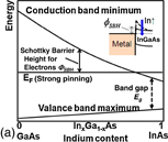
Figure 15(a) schematically shows SBH in InGaAs alloys as a function of the In content in InGaAs.18) The energies of the conduction band and the valence band edges, and the surface EF at the metal/InGaAs interfaces with respect to the vacuum energy level are plotted as the vertical axis. The surface EF level has an almost constant position from the vacuum level with changing In content, while the conduction band edge decreases with an increase in the In content from GaAs toward InAs. As a consequence, the SBH of electrons decreases monotonically with an increase in the In content and can be reduced down to zero, suggesting that InGaAs, particularly with high In contents, has quite a low SBH for electrons and, thus, is an appropriate material for n-MOSFETs with the metal S/D structure. Similarly, it is well known that Ge and GaSb have metal pinning levels close to the valence band edges and have quite a low SBH for holes,17,19,20,110) meaning that Ge and GaSb are suitable for p-MOSFETs with the metal S/D structure.
Download figure:
Standard image High-resolution image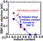
Fig. 15. (a) Schematic diagram of SBH of InGaAs as a function of indium content. (b) SBH of Ni/n-InxGa1−xAs direct contact and Ni–InGaAs alloy/n-InxGa1−xAs formed by RTA at 250 °C for 1 min as a function of indium content, x.
Download figure:
Standard image High-resolution imageOn the other hand, the metal S/D structures strongly require the self-aligned formation process, which is mandatory for deeply scaled MOSFETs, such as the silicide S/D in the Si CMOS process. As for Ge, there are many reports on MOSFETs with a metal-germanide S/D. In particular, the nickel germanide (NiGe) metal S/D has been intensively studied by many groups.187–192) It has been reported that NiGe can be formed by rapid thermal annealing at 200 °C and that excellent Ge p-MOSFETs with a NiGe S/D can be realized. Thus, we have developed self-aligned metal S/D structures by using Ni- and Co-InGaAs alloys formed by the direct reaction of InGaAs with Ni and Co, respectively, for InGaAs n-MOSFETs.123,162,167,169,193,194) It has been found that the Ni–InGaAs alloy layers exhibit a low sheet resistance of approximately 25 Ω/square, which is lower by 1/3 than that of InGaAs layers doped with n-type impurities up to the solid solubility (∼80 Ω/square). Also, it has been confirmed that Ni can be selectively etched by an HCl solution against the Ni–InGaAs alloy, allowing us to employ the salicide-like self-aligned metal S/D formation process. Figure 15(b) shows the experimental results of SBH between Ni–InGaAs and InGaAs as a function of the indium content. The Ni–InGaAs formation was carried out by RTA at 250 °C for 1 min. The results for the Ni/InGaAs contact without any reaction annealing are also shown for comparison. We have confirmed that SBH decreases with an increase in the In content, irrespective of the Ni–InGaAs reaction, and the SBH values of almost 0 eV are obtained at indium contents of 0.7 and 0.8, as expected. These results indicate that SBH engineering using the InGaAs channels with higher indium contents is promising for metal S/D n-MOSFETs.123,193)
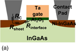
Figure 16(a) schematically shows the components of parasitic S/D resistance (RSD) in the present metal S/D structure, which is composed of S/D sheet resistance (Rsheet), contact resistance with contact via metal (RC), and interface resistance between Ni–InGaAs and InGaAs channels (Rinterface).195,196) The Ni–InGaAs alloy has low Rsheet of ∼250 µΩ cm for a thickness of Ni–InGaAs down to ∼4 nm. On the other hand, RC is quite sensitive to the interface properties between the contact metal and Ni–InGaAs alloys. By employing NH4OH and H2 plasma pre-cleaning for the contact regions and Al/Ti contact metal, which can reduce native oxides at the InGaAs surfaces, RC can be reduced down to 11 Ω µm, corresponding to the specific contact resistivity (ρC) of 5 × 10⁻⁸ Ω cm2.
Download figure:
Standard image High-resolution image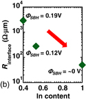
Fig. 16. (a) Schematic view of components of parasitic S/D resistance in InGaAs n-MOSFETs with metal S/D. (b) Extracted Rinterface from InGaAs n-MOSFETs with different In contents as a function of In content.
Download figure:
Standard image High-resolution imageAlso, Fig. 16(b) shows Rinterface for InGaAs n-MOSFETs with different In contents, extracted from the gate length dependence of the InGaAs n-MOSFET resistance and the values of Rsheet and RC. It is found that Rinterface is dramatically reduced down to ∼50 Ω µm by increasing the In content, which is attributable to the SBH free contact behavior in higher In content channels.123,193) The Rinterface value of ∼50 Ω µm for InAs is close to the fundamental limit of Rinterface, given by Landauer's theory on interface conductance.196–198) According to this formulation, the fundamental limit of Rinterface in the degenerate limit is estimated to be 52 Ω µm at a sheet electron concentration of 1013 cm−2 on the semiconductor side. This value is close to the present experimental result, suggesting that sufficiently low Rinterface can be realized for InAs n-MOSFETs with a metal S/D.
We have also confirmed that a similar metal S/D process using metal–semiconductor alloys is applicable to InP199) and GaSb.200–202) It has been found that Ni–GaSb alloy, which can be formed at a low temperature of 250 °C, provides an Rsheet of 10–80 Ω/square and SBH of 0.17 eV for holes.200,201) GaSb p-MOSFETs have also been fabricated and have operated by the self-align process using a Ni–GaSb alloy S/D.202)
3.4. Demonstration of short channel III–V tri-gate MOSFETs
While the ultrathin body structures are mandatory for scaled MOSFETs, a strong concern with decreasing the body thickness (Tbody) is the mobility reduction caused by the body thickness fluctuation scattering.203,204) While the mobility reduction by the body thickness fluctuation scattering has experimentally been identified for UTB-SOI MOSFETs, this scattering becomes much more influential to III–V MOSFETs because of the lower effective mass and larger inversion-layer thickness.156,159,165,166,175,205) Actually, we have clearly observed the rapid mobility reduction of InGaAs-OI n-MOSFETs with thinning of the InGaAs-OI down to less than 10 nm.159,175,205)
Thus, as channel engineering to enhance the mobility in ultrathin body InGaAs-based channels, we have introduced two booster technologies, higher In content (InAs) channels and MOS interface buffers, where lower-In-content buffers sandwich the higher-In-content channels, resulting in the QW InGaAs/InAs/InGaAs-OI channels.167,175,178,205–207) Figure 17(a) shows the schematic cross section of the InGaAs/InAs/InGaAs-OI MOSFETs with a MOS interface buffer layer. The higher In content can lead to higher mobility, because of the smaller effective mass. Also, the QW structure with MOS interface buffers is expected to mitigate the thickness fluctuation scattering, because the electron wave function is more confined into the center channel and, thus, is less influenced by the thickness fluctuation of the total semiconductor channels including the buffer layers. Actually, the fluctuation of the total channel thickness, determined by the thinning etching process, tends to be higher than that of the InAs channel thickness, as determined by epitaxial growth.
Download figure:
Standard image High-resolution image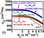
Fig. 17. (a) Schematic cross section of InGaAs/InAs/InGaAs-OI MOSFETs with a MOS interface buffer layer and each physical parameter. (b) Electron effective mobility characteristics of MOSFETs with the In0.53Ga0.47As-OI (20 nm) without MOS interface buffers, the In0.7Ga0.3As-OI (10 nm) without MOS interface buffers, the In0.3Ga0.7As (2 nm)/In0.7Ga0.3As (5 nm)/In0.3Ga0.7As (3 nm) QW-OI channel, and the In0.3Ga0.7As (3 nm)/InAs (3 nm)/In0.3Ga0.7As (3 nm) QW-OI channel as a function of Ns at RT.
Download figure:
Standard image High-resolution imageFigure 17(b) shows the electron effective mobility characteristics of InxGa1−xAs-OI MOSFETs as a function of Ns at RT.175) The mobility of MOSFETs with an In0.3Ga0.7As (2 nm)/In0.7Ga0.3As (5 nm)/In0.3Ga0.7As (3 nm) QW is higher than that of 10-nm-thick In0.7Ga0.3As without any buffers, in spite of the smaller In0.7Ga0.3As thickness, which is evidence of the mitigation of thickness fluctuation scattering by the QW structure with the MOS interface buffers. Also, the In0.3Ga0.7As (3 nm)/InAs (3 nm)/In0.3Ga0.7As (3 nm) QW channel provides a high electron mobility of 3180 cm2 V−1 s−1 at 300 K even with a Tbody of 3 nm, attributed to the combination of the suppression of the thickness fluctuation and the increase in phonon-limited mobility in InAs. Combining this channel structure with the RSD reduction technologies described in the previous section, we fabricated 20-nm-Lch InAs-on-insulator (InAs-OI) n-MOSFETs on Si substrates with a Ni–InGaAs metal S/D.195,196) The devices have provided a high maximum Ion and maximum transconductance (Gm) values of 2.38 mA/µm and 1.95 mS/µm at a drain voltage (VD) of 0.5 V, which are comparable to or higher than those of the recent advanced InGaAs MOSFETs.124,208–217) This high performance is attributable to the better mobility in the higher In-content channels with MOS interface buffers as well as the low RSD realized by the surface cleaning process of Ni–InGaAs surfaces before the contact pad formation.
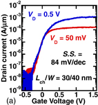
To improve the performance of InAs QW MOSFETs with much stronger SCE immunity, we have fabricated sub-20-nm-Lch tri-gate InGaAs/InAs/InGaAs-OI QW MOSFETs with better electrostatics.206,218) Figure 18(a) shows the schematic structure of the fabricated InGaAs/InAs/InGaAs tri-gate MOSFETs. The channel structure is composed of In0.3Ga0.7As (3 nm)/InAs (3 nm)/In0.3Ga0.7As (3 nm)-OI channel (InAs-OI) structures, shown in Fig. 17, to achieve both high mobility and good SCE control through reduction in scattering probability under the minimized channel thickness.167,175,178,205–207) Also, the S/D is formed by the Ni–InGaAs metal for low RSD. Figures 18(b) and 18(c) show cross-sectional TEM photographs of a fabricated tri-gate MOSFET along the channel length direction and the channel width direction, respectively. The channel length is determined by the distance between the Ni–InGaAs metal source and the drain, evaluated from the energy dispersive X-ray spectroscopy (EDX) profile of Ni shown here. A Fin-like tri-gate channel structure with the top channel width (W) down to 36 nm and the (111) facet side channels, formed by chemical wet etching of the InGaAs layer for W narrowing, is clearly seen.

Fig. 18. (a) Schematic structure of fabricated InGaAs/InAs/InGaAs tri-gate MOSFETs. (b) Cross-sectional TEM photograph of a fabricated tri-gate MOSFET along the channel length direction. (c) Cross-sectional TEM photograph of a fabricated tri-gate MOSFET along the channel width direction.
Download figure:
Standard image High-resolution imageFigures 19(a) and 19(b) show the ID–VG and ID–VD characteristics, respectively, of the MOSFETs with W of ∼40 nm and Lch of 30 nm. Here, ID is normalized by the total length of the top and side channels. Excellent transfer characteristics are obtained with sub-threshold swing (S.S.) of 84 mV/dec, DIBL of 22 mV/V, and Gm,max of 1.64 mS/µm, indicating good MOS interface quality in the (111) side channels. Also, the output characteristics show a maximum Ion of ∼1.3 mA/µm with good current saturation. Figure 20(a) shows the S.S. characteristics with different W. While severe SCEs are observed in In0.3Ga0.7As (3 nm)/InAs (3 nm)/In0.3Ga0.7As (3 nm)-OI MOSFETs with a large W in Lch < 100 nm, S.S. is suppressed in In0.3Ga0.7As/InAs/In0.3Ga0.7As-OI MOSFETs with W smaller than 50 nm. These results strongly indicate that the side gate effect due to the W scaling of ETB-OI MOSFETs can significantly suppress SCEs in Lch < 50 nm.
Download figure:
Standard image High-resolution image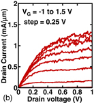
Fig. 19. (a) ID–VG and (b) ID–VD characteristics of a tri-gate In0.3Ga0.7As (3 nm)/InAs (3 nm)/In0.3Ga0.7As (3 nm) QW-OI MOSFET with Lch/W of 30/40 nm.
Download figure:
Standard image High-resolution image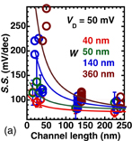
Download figure:
Standard image High-resolution image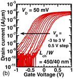
Fig. 20. (a) S.S. characteristics of In0.3Ga0.7As (3 nm)/InAs (3 nm)/In0.3Ga0.7As (3 nm) QW-OI MOSFETs with different W values, as a function of Lch. (b) Substrate bias (VB) dependence of ID–VG curves of In0.3Ga0.7As (3 nm)/InAs (3 nm)/In0.3Ga0.7As (3 nm) QW-OI MOSFETs with Lch/W = 450/40 nm at VD of 50 mV.
Download figure:
Standard image High-resolution imageWe have also examined Vth tunability using substrate bias (VB) control for the present devices with a 40-nm-thick Al2O3 BOX.206,218) Figure 20(b) shows the ID–VG characteristics of In0.3Ga0.7As/InAs/In0.3Ga0.7As-OI MOSFETs with W/Lch of 40/450 nm at VD of 50 mV as a parameter of VB. It is found that the application of VB of ∼3 V can substantially modulate the threshold voltage (Vth) by ∼0.73 V without any degradation of Ion, Ioff, or S.S. characteristics, ascribed to tri-gate structures on ETB-OI. These results strongly suggest that the tri-gate ETB III–V-OI structure is very promising for scaled devices on the Si platform to simultaneously satisfy high performance, high SCE immunity, and Vth tunability.
4. CMOS devices using Ge/III–V materials
4.1. Ge CMOS
Among a variety of CMOS structures using Ge/III–V high mobility materials, shown in Fig. 1, Ge CMOS can be regarded as one of the most promising and realistic CMOS structures,219–222) because (1) high electron and hole mobilities can be obtained for Ge, as shown in Table I, (2) Ge/SiGe p-MOSFETs with the comparatively high performance have already been demonstrated, (3) Ge films grown on Si can be usable for device applications, and (4) a single material can be used for both n- and p-MOSFETs. On the other hand, the realization of high-performance Ge n-MOSFETs can be one of the most critical issues for Ge CMOS. While the recent progress in gate stack technologies based on the Ge oxides, described in Sect. 2.1, has enabled us to significantly enhance the electron mobility of Ge n-MOSFETs, further enhancement of the mobility and optimization of the fabrication processes to overcome the higher current drive in short-channel Ge n-MOSFETs than in existing strained-Si n-MOSFETs are strongly needed.
One of the key technologies for obtaining such high performance Ge n-MOSFETs can be the application of tensile strain into Ge channels and the reduction of the S/D resistance,223–227) in addition to further refinement of the gates stack technologies. Tensile-strained Ge n-MOSFETs with an embedded SiGe S/D have recently been demonstrated.228–230) GeSn buffer technologies are also expected to introduce tensile strain in Ge channels.226,227) The development of the excellent strained-Ge technology combined with UTB Ge structures is strongly expected.
On the other hand, the reduction in the contact resistance of Ge n-MOSFETs could have an essential difficulty among the parasitic resistance in S/D. It is well known that Ge p-MOSFETs can enjoy low contact resistance, because the EF level position at metal/Ge interfaces is strongly pinned near the valence band edge, almost independent of the metal species, leading to quite a low SBH against holes.19,20) While this inherent nature also makes Ge channels suitable for metal S/D p-MOSFETs, this property makes the contact resistance with the n+ Ge S/D quite high because of the high SBH against electrons. In addition to the high SBH, the low solubility of donor impurities in Ge and high diffusion constant of the donors can increase the sheet resistance in impurity-doped Ge S/D regions.231–233) Recent intensive studies on controlling and reducing the SBH against n-Ge as well as doping technologies of high concentration donors into Ge are expected to lead to further reduction in the S/D parasitic resistance of Ge n-MOSFETs.39,234–241)
4.2. III–V CMOS
To realize III–V CMOS, the realization of high-performance III–V p-MOSFETs is a key, in contrast to the Ge CMOS. Thus, much attention has been paid to GaSb-based p-MOSFETs, because of their higher hole mobility. In addition, the application of compressive strain into antimonide materials can be regarded as quite effective in boosting the hole mobility.15,242) There have recently been many reports on GaSb,178,182,202,243–248) InGaSb,168,170,247,249–252) and InSb253–255) p-MOSFETs. Some of them have exhibited fairly good hole effective mobility. Also, similar to the InGaAs/InAs channels described in Sect. 2, GaSb p-MOSFETs with self-aligned Ni–GaSb S/D,181,247) GaSb-OI,177,202) and InGaSb-OI168,170,252) p-MOSFETs have already been demonstrated. However, there are still many technological issues such as the high density of interface defects, poor thermal stability, high leakage current, integration with the Si platform, and the necessity of further improvement in mobility and current drive.
From the viewpoint of CMOS structures, on the other hand, III–V channels are more complicated than Ge, because a single material with both high electron and hole mobilities is rare and, thus, the ones enabling the single-channel CMOS are very limited. One III–V semiconductor system promising for the single material CMOS is InGaSb.250) While sufficiently high performance has not been achieved for InGaSb n-MOSFETs,250) further intensive studies of the InGaSb CMOS is expected.
Another possible option for the III–V CMOS is to integrate As-based III–V n-MOSFETs with Sb-based III–V p-MOSFETs. Nah et al. have demonstrated III–V CMOS operation by combination of InAs n-MOSFETs with InGaSb-OI p-MOSFETs on Si substrates by bonding the two different materials with SiO2/Si substrates through the epitaxial lift-off technique.170) While this approach seems quite interesting,170,252) the separated formation of the two different materials for the channels of n-MOSFETs and p-MOSFETs could be complicated in terms of device integration. Thus, any one structure combining InAs n-MOSFETs and GaSb p-MOSFETs is also interesting. An InAs/GaSb core–shell-type CMOS has been realized.256,257) We have also proposed and demonstrated a novel single structure III–V CMOS composed of GaSb/InAs heterostructures.181) It has been found that the CMOS operation of the InAs/GaSb-OI channel is realized by using ultrathin InAs layers, enabling the quantum confinement of the InAs channel and tight gate control. QW InAs/GaSb-OI on Si structures have been fabricated by using DWB. We have experimentally demonstrated both n- and p-MOSFET operation for an identical InAs/GaSb-OI transistor by choosing the appropriate thickness of InAs and GaSb channel layers, suggesting that the developed InAs/GaSb-OI MOSFETs can open up a new and simple way to realize III–V CMOS transistors on the Si platform. However, there are still many issues to be solved, such as the high leakage current, and significant mobility reduction due to InAs and GaSb UTB channels. Since the activities of the development of III–V CMOS on the Si platform are very few,170,181,252) further intensive studies on realistic CMOS integration are necessary in addition to the fundamental understanding of MOS interface properties and carrier transport properties in Sb-based III–V MOSFETs.
4.3. III–V/Ge CMOS
As described in Sect. 1 and Fig. 1, the ultimate CMOS structure can be the combination of InGaAs/InAs n-MOSFETs and Ge p-MOSFETs, judging from the fundamental properties of the semiconductors. In addition to high carrier mobility, a low or almost zero SBH for electrons in InGaAs/InAs123,193) and for holes in Ge19,20) is effective in reducing the parasitic resistance of the S/D, which is important for scaled CMOS devices with ultrashort Lch. However, one drawback of this structure is the complexity of the integration process to form the two different channel materials on Si substrates.
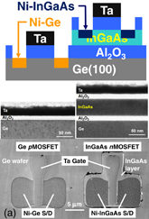
To realize this CMOS structure, we have employed wafer bonding of In0.53Ga0.47As thin films with Ge substrates through an Al2O3 BOX.163,172) The Al2O3-based gate stacks and Ni-semiconductor alloy S/D, described in Sects. 2.1 and 3.3, have been applied to both InGaAs-OI n-MOSFETs and Ge p-MOSFETs as the common gate stack and S/D formation technologies. Figure 21(a) shows the schematic cross section of the fabricated devices and a photograph of the top view of III–V/Ge MOS transistors (the right transistor is the InGaAs-OI n-MOSFET with a Ni–InGaAs metal S/D and the left transistor is the Ge p-MOSFET with a Ni–Ge metal S/D) on an InGaAs-OI-on-Ge wafer. Figure 21(a) also shows cross sectional TEM photographs of the III–V/Ge CMOS transistors. Here, the left photograph shows the gate stack region of the Ge p-MOSFET and the right photograph shows the stack structures of the Ta/Al2O3/InGaAs gate stack on Ge with Al2O3 buried oxides. It has been confirmed that the flat and uniform structures are fabricated by the DWB process. Also, we have confirmed that the Ni–InGaAs and Ni–Ge metal S/Ds are formed without any connection with the Ta gate. Figure 21(b) shows the ID–VD characteristics of a 20-nm-thick In0.53Ga0.47As-OI n-MOSFET and a Ge p-MOSFET. The normal MOSFET operation is observed for both devices on the same Ge wafer. We have confirmed the high electron and hole mobilities of 1800 and 260 cm2 V−1 s−1 and the mobility enhancement against Si MOSFETs of 3.5× and 2.3× for the InGaAs-OI n-MOSFET and the Ge p-MOSFET, respectively.
Download figure:
Standard image High-resolution image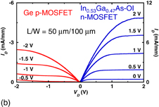
Fig. 21. (a) Top view of III–V/Ge CMOS transistors (the right transistor is the InGaAs-OI n-MOSFET with a Ni–InGaAs metal S/D and the left transistor is the Ge p-MOSFET with a Ni–Ge metal S/D) and cross-sectional TEM photographs of the bonded substrate and the schematic cross section of the III–V/Ge CMOS transistors. (b) ID–VD characteristics of a Ge p-MOSFET and a 20-nm-thick InGaAs-OI n-MOSFET.
Download figure:
Standard image High-resolution image
Also, Czornomaz and co-workers have recently achieved the CMOS inverter operation using InGaAs-OI n-MOSFETs and SGOI p-MOSFETs by wafer bonding of InGaAs layers with SGOI layers on Si substrates.173,180) Similarly, Irisawa and co-workers have also demonstrated the real circuit operation of CMOS composed of InGaAs-OI wire n-MOSFETs and SGOI wire p-MOSFETs by three-dimensional (3D) vertical stacking of InGaAs-OI nMOSFETs on SGOI p-MOSFETs through wafer bonding.174,184) The operation of 21-stage CMOS ring oscillators and independent Vth control for n- and p-MOSFETs have been demonstrated for this CMOS structure realized by sequential 3D integration. The low thermal budget for III–V/Ge channel MOSFETs is suitable for devices in 3D stack integration. Further progress in the technologies to overcome any possible problems in the CMOS integration is strongly expected for the III–V/Ge CMOS.
5. Conclusions
CMOS utilizing high-mobility Ge/III–V channels on the Si platform is expected to be one of the promising devices for high-performance and low-power logic LSIs in the future. To realize the III–V/Ge logic CMOS, there are many critical issues including the technologies of the gate stacks, the channel formation, low resistivity S/D formation, formation of UTB channels with high immunity against SCEs, and CMOS integration. However, the device/process/integration technologies of Ge/III–V n- and p-MOSFETs for satisfying these requirements for future node MOSFETs have not been established yet. The reality of a variety of CMOS structures is dependent on the progress of these device and process technologies. In this paper, we have addressed several key technologies to realize the III–V/Ge CMOS for logic LSIs on the basis of our recent achievements.
For Ge MOSFETs, GeOx/Ge interfaces formed by post plasma oxidation were shown to realize thin EOT, low Dit, and high mobility. HfO2/Al2O3/GeOx/Ge gate stacks have exhibited high electron and hole mobilities under an EOT thinner than 1 nm. The reduction in interface roughness and interface state density through low temperature plasma oxidation and D annealing, respectively, have effectively enhanced the mobility in the high Ns region. Also, the Ge condensation method was mainly described for UTB GOI/SGOI formation on Si substrates with emphasis on the effectiveness of the condensation using tensile strained SOI substrates.
For III–V MOSFETs, the MOS interface control based on ALD Al2O3 ILs was employed to realize HfO2/Al2O3/InGaAs stacks with a low Dit and a CET of 1.08 nm. Direct wafer bonding technology has been employed for III–V channel formation on Si substrates. The wafer bonding using III–V epitaxial films on Si substrate donor wafers allows us to apply this technology to the Si platform based on 300 mm wafers or larger. The planar UTB/UTBOX-based multi-gate structures to suppress SCEs and to control Vth in a static and/or dynamic way have been realized with the combination of the InAs-OI QW channel structure and the Ni–III–V metal S/D technology. The 20-nm-Lch tri-gate InAs-OI QW MOSFETs have been demonstrated with good electrostatics, a low S.S. value and a high current drive.
Based on the present viable device technologies, plausible CMOS structures using III–V/Ge channels have been discussed. The present status and critical issues for realizing Ge CMOS, III–V CMOS, and III–V/Ge hybrid CMOS have been addressed referring to typical examples of demonstrated CMOS results.
As a result, we can conclude that UTB-based III–V/Ge MOSFETs on the Si CMOS platform can be strong candidate device structures under the 10 nm technology node and beyond. To introduce III–V/Ge MOSFETs into real LSIs, on the other hand, further fundamental studies including the understanding of the carrier transport properties in the UTB and ultrashort-channel devices, physical mechanisms of MOS interface defects, and the reliability physics of any possible degradations of the performance are indispensable. Also, ultimate refinements of the process technologies allowing atomic-scale material control such as defect-less high material quality and hyperfine surface flatness are strongly required. Further progress in the science and technologies for realizing III–V/Ge CMOS is highly expected.
Acknowledgments
This work was partly supported by a Grant-in-Aid for Scientific Research (No. 23246058) from MEXT, Innovation Research Project on Nano Electronics Materials and Structures, and Research and Development Program for Innovative Energy Efficiency Technology from NEDO, and the JST-CREST. The authors would like to thank Dr. T. Hoshii and Professor R. Nakane of the University of Tokyo, Dr. T. Yasuda, Dr. T. Maeda, Dr. W. Jevasuwan, Dr. N. Miyata, Dr. Y. Urabe, and Dr. H. Takagi of AIST, Dr. A. Ohtake of NIMS, Dr. M. Hata, Dr. O. Ichikawa, Dr. N. Fukuhara, and Dr. H. Yamada of Sumitomo Chemical, Dr. H. Yokoyama of NTT and Dr. J. Li and Dr. Y.-C. Kao of IntelliEPI Inc. for their collaborations. We would also like to thank SOITECH for providing sSOI and XsSOI substrates.