Abstract
Power semiconductor devices are key components in power conversion systems. Silicon carbide (SiC) has received increasing attention as a wide-bandgap semiconductor suitable for high-voltage and low-loss power devices. Through recent progress in the crystal growth and process technology of SiC, the production of medium-voltage (600–1700 V) SiC Schottky barrier diodes (SBDs) and power metal–oxide–semiconductor field-effect transistors (MOSFETs) has started. However, basic understanding of the material properties, defect electronics, and the reliability of SiC devices is still poor. In this review paper, the features and present status of SiC power devices are briefly described. Then, several important aspects of the material science and device physics of SiC, such as impurity doping, extended and point defects, and the impact of such defects on device performance and reliability, are reviewed. Fundamental issues regarding SiC SBDs and power MOSFETs are also discussed.
Export citation and abstract BibTeX RIS
1. Introduction
The improvement of energy efficiency (reduction of power consumption and dissipation) is one of the most critical problems of this century. In 2010, the world average ratio of electrical energy consumption to total energy consumption was about 20%.1) This ratio is expected to rapidly increase in the future. Regardless of the means by which electrical power is generated, power conditioning and conversion are required for cost-effective and efficient delivery to the loads. It is estimated that more than 50% of all electrical power flows through some form of power conversion. Electric power is regulated and converted so that it can be supplied to the loads in an optimum form. Electric power conversion includes AC–DC, DC–AC, DC–DC (voltage conversion), and AC–AC conversion (voltage or frequency conversion).2) The efficiency of power conversion is typically 85–95% using currently available technology, which is not high enough, because approximately 10% of the electric power is lost as heat at every power conversion.
In general, the efficiency of power electronics is mainly limited by the performance of semiconductor devices. As shown in Fig. 1, major applications of power devices include power supplies, motor control, heating, robotics, electric/hybrid vehicles, traction, lighting ballasts, and electric power transmission. The development of high-voltage and low-loss power devices is also essential for the construction of future smart grids.

Fig. 1. Major application areas of power devices plotted as a function of rated voltage.
Download figure:
Standard image High-resolution imageSilicon (Si) is currently the most commonly used semiconductor for power devices. The performance of Si power switching devices has been significantly improved through the development of power metal–oxide–semiconductor field-effect transistors (MOSFETs) and insulated gate bipolar transistors (IGBTs).3,4) Progress in Si LSI technology and in device simulation has had a great impact on the development of Si power devices in recent decades. However, now that Si power device technology is relatively mature, it is not easy to achieve innovative breakthroughs using this technology.
Silicon carbide (SiC) is a IV–IV compound material with unique physical and chemical properties. The strong chemical bonding between Si and C atoms gives this material high hardness, chemical inertness, and high thermal conductivity.5) The strong bonding also provides this material with a wide bandgap and high critical (breakdown) electric field strength. Among the many wide-bandgap semiconductors, SiC is rather exceptional because it makes both n- and p-type control across a wide doping range (1014–1019 cm−3) relatively easy. The ability of SiC to form silicon dioxide (SiO2) as a native oxide is another important advantage for device fabrication. Because of these properties, SiC has been developed as a semiconductor for high-power and high-temperature electronics.6–13)
However, the physical and chemical stability of SiC made crystal growth extremely difficult and severely hampered the development of SiC semiconductor devices and their electronic applications in the last century. The existence of various SiC crystal structures with different stacking sequences (otherwise known as "polytypism")14) has also been an obstacle to the growth of electronic-grade SiC crystals. Among the numerous SiC "polytypes", 4H-SiC has been the choice for power devices9,12,15–18) owing to the availability of high-quality epitaxial wafers and superior physical properties such as its high breakdown electric field strength,19) high electron mobility, and low anisotropy.20) Figure 2(a) shows a schematic of the crystal structure of 4H-SiC, where the open and closed circles denote the Si and C atoms, respectively. This polytype exhibits a hexagonal structure with four Si–C bilayers inside the unit cell. That is why this polytype is called "4H" according to the Ramsdell notation.14) This stacking sequence is a kind of mixture of zincblende and wurtzite structures. Since 4H-SiC is the default SiC polytype for electronic applications, the term "SiC" will hereafter represent 4H-SiC in this paper, unless otherwise specified. Figure 2(b) illustrates the hexagonal unit cell of SiC, where the major crystal faces, (0001),  ,
,  , and
, and  , are indicated. Here, (0001) and
  are called the "Si face" and "C face", respectively. Note that the standard face of commercial SiC wafers is almost exclusively (0001).

Download figure:
Standard image High-resolution image
Fig. 2. (a) Schematic crystal structure of 4H-SiC, where the open and closed circles denote the Si and C atoms, respectively. (b) Hexagonal cell of SiC, where the major crystal faces, (0001),  ,
,  , and
, and  , are indicated.
Download figure:
Standard image High-resolution imageTable I tabulates the main physical properties of SiC and Si at room temperature. The unique properties of SiC include its three times larger bandgap, roughly ten times higher breakdown electric field strength, and three times higher thermal conductivity as compared with Si. Note that in SiC (i.e., 4H-SiC),20) the electron mobility along the 〈0001〉 direction is about 15–20% higher than that perpendicular to 〈0001〉, which is beneficial for the development of vertical power devices on standard SiC{0001} wafers.
Table I. Main physical properties of SiC (4H-SiC) and Si at room temperature.
| SiC | Si | |
|---|---|---|
| Bandgap (eV) | 3.26 | 1.12 |
| Electron mobility for high-purity material (cm2 V−1 s−1) | ||
| μ parallel to c-axis | 1200 | 1350 |
| μ perpendicular to c-axis | 1020 | 1350 |
| Hole mobility (cm2 V−1 s−1) | 120 | 450 |
| Electron saturated drift velocity (cm/s) | 2.2 × 10⁷ | 1.0 × 10⁷ |
| Hole saturated drift velocity (cm/s) | (∼1.3 × 10⁷) | 9 × 10⁶ |
| Breakdown electric field for material with a doping density of 1016 cm−3 (MV/cm) | ||
| EB parallel to c-axis | 2.8 | 0.3 |
| EB perpendicular to c-axis | 2.2 | 0.3 |
| Thermal conductivity (W cm−1 K−1) | 3.3–4.9 | 1.3–1.5 |
| Relative dielectric constant | 9.8 | 11.9 |
Both SiC and gallium nitride (GaN) are wide-bandgap semiconductors, which are attractive for advanced power devices because of their superior physical properties. Although it is difficult to predict how Si-, SiC-, and GaN-based power devices will compete, SiC power devices are more attractive for high-voltage applications owing to the availability of reasonably high-quality epitaxial wafers and the more mature process technology than that of GaN. On the other hand, GaN-based lateral switching devices fabricated on GaN heteroepitaxially grown on large Si wafers show much promise for relatively low-voltage applications.21,22) The performance, reliability, and cost of SiC and GaN power devices will be determined depending on advances in growth and device technologies of the two materials. The present review focuses on fundamental issues regarding SiC for power device applications. The present understanding and future challenges of the material science and device physics are discussed.
2. Features of SiC power devices
Power devices are key components in power conversion systems. Figure 3 depicts a typical power conversion circuit (inverter) employed for three-phase motor control. In each phase with positive and negative polarities, the switching operation of a pair consisting of a transistor (switching device) and diode regulates the electric power supplied to the motor. In many applications, both rectifiers (diodes) and switching devices having the same rating of voltage and current are required. In any case, power devices are either "on-state" or "off-state", similar to logic devices in integrated circuits. A switching operation is performed between the on- and off-states, but the switching frequency is usually not very high, in the range from 1 kHz to a few 100 kHz.

Fig. 3. Typical circuit of three-phase power inverter for motor control.
Download figure:
Standard image High-resolution imageFigure 4 schematizes the current–voltage characteristics of (a) a power rectifier (diode) and (b) a power switching device, where the ideal and real characteristics are compared. In ideal devices, a "zero" voltage drop in the on-state and "zero" leakage current (and "infinite" breakdown voltage) in the off-state are expected. However, real devices exhibit a finite semiconductor resistance and a finite leakage current (and a maximum voltage limited by breakdown), which are the main cause of the on-state and off-state loss, respectively. Furthermore, any transient behavior during the switching operation results in switching loss. Therefore, the major requirements for power devices include (i) low on-state voltage (low on-resistance), (ii) low leakage current, and (iii) fast switching with minimum current/voltage transients, which are directly linked to the on-state loss, off-state loss, and switching loss, respectively. A high blocking voltage can, of course, be a requirement, depending on the application. Furthermore, a large safe-operation area (robustness) and reliability are also important because power devices must withstand, for example, simultaneous high-voltage and high-current stress for a certain period without any degradation. In all these aspects, SiC shows promising potential, as described below.

Download figure:
Standard image High-resolution image
Fig. 4. Current–voltage characteristics of (a) power diode and (b) power switching device, where the ideal and real characteristics are compared.
Download figure:
Standard image High-resolution imageFigure 5 schematically illustrates the electric field distribution in a one-sided abrupt junction for SiC and Si at the same breakdown voltage. Because the breakdown field strength for SiC is about ten times higher than that for Si, the thicknesses of the voltage-blocking layers in SiC power devices can be one-tenth those in Si devices, and their doping concentrations can be two orders of magnitude higher than in their Si counterparts for the same blocking voltage. Thus, the drift-layer resistance in unipolar devices can be reduced by 2–3 orders of magnitude at any given blocking voltage by utilizing SiC instead of Si. This is particularly important for high-voltage devices because the drift-layer resistance (Rdrift) increases with the blocking voltage (VB) in proportion to  and is the dominant factor determining the total specific on-resistance (RON) of power devices.3,4) The on-state loss (PON) of a power device without a built-in voltage is given by
  , where JON is the on-state current density (typically 100–300 A/cm2 at the rated current). Thus, the extremely low drift resistance of SiC devices contributes to the reduction of the on-state loss. Figure 6 plots the minimum specific on-resistance (drift-layer resistance) against the blocking voltage for Si and SiC unipolar devices. The minimum specific on-resistance (drift-layer resistance) is given by4,12,23)

where ε, μ, and EB are the dielectric constant, mobility, and breakdown field strength, respectively. Here, η is the ionization ratio for the dopants at room temperature. In the case of lightly-doped n-type SiC, η is about 0.85–1.0 owing to the relatively shallow nitrogen donors. This is especially important for wide-bandgap semiconductors, where the incomplete ionization of dopants is often observed. In fact, p-type SiC Schottky barrier diodes (SBDs) and power MOSFETs cannot compete with Si because of the low hole mobility and small ionization ratio for aluminum (Al) acceptors at room temperature. In Fig. 6, the doping-dependent mobility and breakdown field were taken into account to calculate the drift-layer resistance. The above-mentioned benefits of SiC power devices can be clearly recognized in this plot. Although the drift-layer resistance (Rdrift) is proportional to  in Eq. (1), the actual resistance increases in proportion to
  , as seen in Fig. 6, because the breakdown field strength decreases in the lightly-doped materials employed for high-voltage devices. The dependence of the breakdown electric field strength on doping density is discussed in Sect. 4.

Fig. 5. Electric field distribution in a one-sided abrupt junction for SiC and Si at the same breakdown voltage. Because of the approximately ten times higher breakdown field strength of SiC than that of Si, the thickness of the voltage-blocking layers for SiC power devices can be reduced tenfold and the doping concentration can be increased by two orders of magnitude compared with the Si counterpart with the same blocking voltage.
Download figure:
Standard image High-resolution image
Fig. 6. Minimum specific on-resistance (drift-layer resistance) for Si and SiC unipolar devices (so-called "Si limit" and "SiC limit") versus the blocking voltage. Experimental data for SiC power MOSFETs and JFETs recently reported are plotted.
Download figure:
Standard image High-resolution imageAnother important feature of SiC power devices is fast switching with minimum reverse recovery (little current overshoot). For medium- and high-voltage applications, Si bipolar devices such as PiN diodes, IGBTs, bipolar junction transistors (BJTs), and thyristors are employed because the high on-resistance can be significantly reduced by a conductivity modulation effect through minority carrier injection.4) Bipolar power devices, however, suffer from minority carrier storage, leading to a slow switching speed and large reverse recovery in the turn-off operation. For these applications, SiC unipolar devices such as SBDs and FETs are an ideal choice since the on-resistance of these devices is low and minority carrier storage is absent. Even SiC bipolar devices can offer fast switching because the voltage-blocking region is about ten times thinner and thus the stored charge in the region is about ten times smaller compared with Si bipolar devices.12,13)
Owing to the wide bandgap and chemical stability of SiC, SiC electronic devices are operational at high temperatures (>250 °C). This is attractive in that it helps to avoid bulky cooling units, which are often required in Si-based power converters. Note that SiC devices themselves can operate even at 500 °C or higher,24,25) but performance factors such as their on-resistance generally degrade at such high temperatures. Packaging technology represents another issue in the commercialization of high-temperature operational SiC power devices.
Figure 7 illustrates the structures of major SiC power devices that have been developed. These device structures are basically similar to those of Si power devices, but some modifications have been made due to the unique properties and problems of the current process technology. For example, impurity doping by a diffusion process is unrealistic owing to the extremely small diffusion constants of dopants in SiC.5,12) Thus, impurity doping is performed by either epitaxial growth or ion implantation. In SiC, a high density of deep levels and extended defects remains inside the ion-implanted region as well as the implant-tail region, even after high-temperature activation annealing. As a consequence, the carrier lifetimes near the implanted junction are very short (<0.1 µs), which is not desirable for bipolar devices, where efficient carrier injection and diffusion are essential. Therefore, pn junctions in SiC bipolar devices, such as PiN diodes, BJTs, and thyristors, are fabricated exclusively by epitaxial growth. For the fabrication of SiC unipolar devices, such as SBDs and MOSFETs, however, ion implantation is a very useful technique because nearly ideal breakdown characteristics can be obtained with implanted junctions and no carrier injection is involved in the normal operation of unipolar devices.12,13)

Fig. 7. Schematic structures of various SiC power devices currently developed. (a) Schottky barrier diode (SBD), (b) PiN diode, (c) double-implanted MOSFET (DIMOSFET), (d) trench MOSFET, (e) Junction FET (JFET), (f) bipolar junction transistor (BJT), (g) thyristor, (h) n-channel insulated gate bipolar transistor (IGBT).
Download figure:
Standard image High-resolution imageFigure 8 shows the major territories of individual unipolar and bipolar power devices for Si and SiC in terms of the rated blocking voltage.26) The boundary between unipolar and bipolar devices is located at 300–600 V in the case of Si power devices. In SiC power devices, this boundary is shifted toward a blocking voltage that is about ten times higher, namely several kV. It is expected that SiC unipolar devices will replace Si bipolar devices in the blocking-voltage range from 300 V to about 6500 V. SiC bipolar devices will be attractive for ultrahigh-voltage applications above 10 kV.

Fig. 8. Major territories of individual unipolar and bipolar power devices for Si and SiC in terms of the rated blocking voltage.
Download figure:
Standard image High-resolution image3. Present status of SiC power devices
Since the 1980's, sustained effort has been directed toward developing SiC material and device technology. Because device-quality SiC with a reasonable size was not available for many years, the breakthroughs in SiC crystal growth achieved in the 1980's eventually triggered device development. Tairov and Tsvetkov reported the basic concept of, and successful experimental data on, the so-called "seeded sublimation technique" (or "modified Lely method").27,28) This technique was refined by Carter and coworkers, and the first commercial SiC wafers were released in 1991.29) Low-resistivity n-type SiC wafers with a diameter of 100–150 mm are currently commercially available. The high-quality homoepitaxial growth of SiC was achieved by utilizing step-flow growth on off-axis {0001} substrates by chemical vapor deposition (CVD).30,31) In the epitaxial growth of SiC, perfect replication of the SiC polytype without any polytype mixing is important and was first realized by step-flow growth (called "step-controlled epitaxy").10,30,32) Since wide-range n- and p-type doping is easy with this growth technique, the availability of epitaxial wafers with the desired doping density and thickness has accelerated device development since the 1990's.
Matus et al. reported a 1 kV 6H-SiC pn diode and its rectification operation up to 600 °C.33) The author's group demonstrated a 1 kV 6H-SiC SBD with a low specific on-resistance and 400 °C rectification in 1993.34) In 1994, the on-resistance of high-voltage SiC SBDs was markedly reduced by using 4H-SiC.35) After structure and process optimization, the first SiC SBD products were released in 2001.36) One of the typical applications of SiC SBDs has been as fast diodes employed in the power-factor-correction circuit of switching-mode power supplies.36) Because of the negligibly small reverse recovery of SiC SBDs, the switching loss can be dramatically reduced and the switching frequency can be increased, leading to the downsizing of passive components. The market for SiC SBDs has grown rapidly over the last several years, and SiC SBDs are employed in a variety of power systems, including power supplies, photovoltaic converters, air conditioners, and motor controls for elevators and railcars.37) In research and development, the maximum blocking voltage of SiC diodes has exceeded 25 kV.38,39)
In conjunction with the development of high-voltage SiC diodes, the fabrication of vertical SiC switching devices started in the early 1990's. In 1993, a vertical trench MOSFET using 6H-SiC was demonstrated by Palmour et al.40) Palmour and coworkers also extensively developed 4H-SiC trench MOSFETs, thyristors, and BJTs as important steps towards high-power electronics.41) In 1997, the first planar double-implanted MOSFET (DIMOSFET) using SiC with a blocking voltage of 760 V and a low on-resistance was reported by Cooper and coworkers.42) This group demonstrated a 1.4 kV–15 mΩ cm2 SiC trench MOSFET with a number of innovative design features in 1998.43) A 660 V–1.8 mΩ cm2 SiC MOSFET with a unique channel design was demonstrated in 2006.44) To avoid problems at the SiC MOS interface, vertical junction FETs (JFETs) were developed,45,46) leading to the commercialization of SiC power JFETs in 2006.36) Following the steady improvement of MOS channel mobility and oxide reliability, SiC power DIMOSFETs have been commercially available since 2010.29,47) These devices are well accepted by the market, and industry is now reaping the benefits of SiC power switches. For example, the volume and weight of a power supply or inverter can be reduced by a factor of 2–10, depending on the extent to which SiC components are employed. In addition to the size and weight reduction, a substantial reduction in power dissipation has been confirmed, leading to improved efficiency in electric power conversion systems owing to the use of SiC components. In research and development, double-trench MOSFETs with a very low on-resistance of below 1 mΩ cm2,48) as well as 10 kV DIMOSFETs49) have been demonstrated. However, these SiC power switching devices require further improvement in performance and cost reduction. As examples of ultrahigh-voltage switching devices, 15–20 kV thyristors, IGBTs, and BJTs have been demonstrated.38,50,51) For more detail, please see recent conference proceedings.52) Figure 6 plots the on-resistance and breakdown voltage of recently reported SiC power FETs. Although a gap exists between the theoretical limit and experimental data, especially in relatively low-voltage (600–1200 V) devices, the performance is orders of magnitude better than the Si limit. Note that the performance of SiC SBDs is closer to the theoretical limit of SiC (not shown).
It should be pointed out, however, that the basic understanding of the material science and device physics in SiC is still poor compared with Si technology. For example, many of its physical properties, which are important for accurate device simulation, are unknown. The behavior of defects and their impact on device performance and reliability are under investigation. The mechanism of defect formation during device processing steps such as oxidation and ion implantation remains poorly understood. Furthermore, several unique features of device physics that are observed in SiC but not observed in Si can be common in wide-bandgap semiconductors. For example, the dominant process of carrier generation in a space-charge region as well as the breakdown mechanism of SiC devices may be very different from those of Si devices because of the different bandgap and about ten times higher electric field strength for SiC. The main purpose of this paper is to present a basic understanding of SiC technology.
4. Important aspects associated with material properties
The major physical properties of SiC are tabulated in Table I. In this section, a few electronic properties peculiar to SiC (or wide bandgap semiconductors) are briefly discussed. Because of its wide bandgap, the intrinsic carrier density (ni) in SiC is extremely low, 5 × 10⁻⁹ cm−3 at room temperature, while the corresponding value for Si is 1 × 1010 cm−3. An Arrhenius plot of the intrinsic carrier densities for SiC and Si is shown in Fig. 9. In general, carrier generation is proportional to  in the case of band-to-band generation and to ni in the case of generation via a deep level.53) This is the main reason why SiC devices exhibit a low leakage current even at elevated temperatures. Furthermore, it is of interest to estimate the equilibrium minority carrier density in SiC. Consider n-type SiC having an electron density of 1 × 1016 cm−3, for example. The equilibrium hole density in this n-type SiC can be estimated to be (5 × 10⁻⁹ cm−3)2/(1 × 1016 cm−3) = 2.5 × 10⁻³³ cm−3 at room temperature. Therefore, it is reasonable to assume that no minority carriers are present in SiC unless intentional carrier injection or excitation is performed. No minority carriers are involved during the on-state operation of SiC unipolar devices, which is not the case for Si SBDs. In a SiC MOS capacitor, no inversion layer is created even if a sufficiently large bias voltage is applied, which leads to the appearance of deep depletion because of the absence of minority carriers. These facts must be taken into account in analyzing the characteristics of SiC devices. Through advances in crystal growth and defect engineering, semi-insulating SiC (SI-SiC) wafers have become commercially available. When the Fermi level is pinned at 1.0 eV below the conduction band edge (or above the valence band edge), the majority carrier density is estimated to be as low as about 200 cm−3. Indeed, the resistivity of commercial SI-SiC wafers is extraordinarily high, over 1011 Ω cm,54) which is useful for the development of high-frequency devices55) and high-temperature integrated circuits.56)

Fig. 9. Arrhenius plot of the intrinsic carrier density for SiC and Si.
Download figure:
Standard image High-resolution imageIn conjunction with the extremely small intrinsic carrier density, the Fermi level does not approach the midgap (intrinsic level) in SiC, even at high temperatures. Figure 10 plots the Fermi level for nitrogen- or aluminum-doped SiC as a function of temperature and impurity density, taking into account the temperature dependence of the bandgap and the incomplete ionization of dopants at low temperatures.12) Figure 10 indicates that chemical reactions and defect stability in SiC crystals may exhibit a clear conduction type or doping density dependence during high-temperature treatment. It has been reported, for example, that the thermal oxidation rate for SiC at 1100–1300 °C is dependent on the conduction type and doping density.57) A theoretical study has predicted that the formation energy and migration (diffusion) barrier of point defects in SiC strongly depend on the Fermi level.58) In SiC, this Fermi level dependence is maintained during high-temperature treatment above 1000 °C.

Fig. 10. Fermi level for nitrogen- or aluminum-doped SiC as a function of temperature and impurity density, taking into account the temperature dependence of the bandgap and the incomplete ionization of dopants at low temperatures.
Download figure:
Standard image High-resolution imageFigure 11 plots the breakdown electric field strength versus the doping density for 4H-SiC〈0001〉, 6H-SiC〈0001〉, and 3C-SiC〈111〉.12,19,59,60) The data for Si are also shown for comparison. 4H- and 6H-SiC exhibit approximately 8–10 times higher breakdown field strengths than Si at a given doping density, while the field strength for 3C-SiC is only 3–4 times higher because this polytype has a relatively small bandgap (similar to gallium phosphide). It should be noted that the breakdown field strength is strongly dependent on the doping density, as shown in Fig. 11. As the doping density is increased, the width of the space-charge region as well as the distance over which carriers are accelerated both decrease. Furthermore, the mobility is reduced in highly doped materials because of enhanced impurity scattering. These are the reasons why the breakdown electric field strength increases with increasing doping density. As shown in Fig. 11, the breakdown electric field for 6H-SiC〈0001〉 is slightly higher than that for 4H-SiC〈0001〉 despite the smaller bandgap of the former (Eg = 3.02 eV for 6H-SiC and 3.26 eV for 4H-SiC). It is known that 6H-SiC exhibits strong anisotropy in carrier transport, and the electron mobility along the 〈0001〉 direction is unusually low, about 100 cm2 V−1 s−1, even in a high-purity material.20) The narrow width of the conduction band in 6H-SiC also helps to increase the breakdown electric field strength for 6H-SiC〈0001〉. The breakdown field strength for 6H-SiC is only half of that for 6H-SiC〈0001〉.61) The anisotropy in the breakdown field strength for 4H-SiC is smaller, and the field strength for 4H-SiC
 is only 20–25% lower than that for 4H-SiC〈0001〉.62,63) Note that the breakdown field strength is also slightly anisotropic in Si and gallium arsenide (GaAs).

Fig. 11. Breakdown electric field strength versus doping density for 4H-SiC〈0001〉, 6H-SiC〈0001〉, and 3C-SiC〈111〉. The data for Si are also shown for comparison.
Download figure:
Standard image High-resolution imageThe breakdown field strength is a convenient physical property to use for estimating the ideal breakdown voltage. However, the breakdown field strength is valid only for junctions with non-punch-through structures. When considering punch-through structures, which are common in power devices, the breakdown field strength shown in Fig. 11 does not give the correct breakdown voltage. In this case, simulation of the leakage current or calculation of the ionization integral using a device simulator is required to determine the ideal breakdown voltage.4) To this end, accurate determination of the impact ionization coefficients in SiC has been investigated.64,65)
5. Impurity doping during crystal growth
In SiC, nitrogen (N) or phosphorus (P) is employed for n-type doping, while aluminum (Al) is used for p-type doping. Although boron (B) was also previously employed as an acceptor, it is currently not preferred because of its large ionization energy (∼300 meV),66) its abnormal diffusion,66–68) and the generation of a boron-related deep level (D center).66,67) Although gallium and arsenic work as acceptors and donors, respectively, their ionization energies are relatively large and their solubility limits are low. Nitrogen substitutes at carbon sublattice sites, while phosphorus, aluminum, and boron substitute at silicon sublattice sites. The ionization energies and solubility limits of nitrogen, phosphorus, aluminum, and boron in 4H-SiC are listed in Table II.66,69–76) In SiC, the ionization energies for dopants depend on the lattice site, in particular, whether the site is hexagonal or cubic (site effect).69) In the case of nitrogen or phosphorus doping, the ionization energy for the donors is relatively small, and the ionization ratio for donors at room temperature is reasonably high, ranging from about 80% to nearly 100%, depending on the doping density. Conversely, the ionization energy for aluminum is large (200 meV), and incomplete ionization (5–30%) of acceptors is observed at room temperature. Note that the ionization energy decreases when the doping density is increased as a result of bandgap shrinkage and the formation of an impurity band. Above a dopant density of 1019 cm−3, the ionization energy decreases sharply. As a result, near-perfect ionization is observed in heavily aluminum-doped SiC (>4 × 1020 cm−3) despite the relatively large ionization energy of aluminum.77,78)
Table II. Ionization energies and solubility limits of nitrogen (N), phosphorus (P), aluminum (Al), and boron (B) in SiC.66,69–76) For N, P, and Al, the ionization energies at the hexagonal/cubic sites are indicated.
| N | P | Al | B (shallow) | |
|---|---|---|---|---|
| Ionization energy (meV) | 61/126 | 60/120 | 198/201 | 280–300 |
| Solubility limit (cm−3) | 2 × 10²⁰ | (∼1 × 10²¹) | 1 × 10²¹ | 2 × 10¹⁹ |
In general, one can observe a similar trend in dopant incorporation irrespective of the SiC growth technique: nitrogen incorporation is significantly higher for growth on  than on (0001), and the opposite tendency [higher on (0001)] is true for aluminum incorporation. This polarity effect originates from the surface kinetics during growth. Because nitrogen substitutes at carbon lattice sites, a nitrogen atom adsorbed onto a
  surface is bound to three underlying silicon atoms, while it is only bound to one silicon atom on a (0001) surface. Thus, the desorption of nitrogen atoms from
  is presumably much less extensive than from (0001) (note that the nitrogen vapor pressure is very high at the growth temperature of SiC). This may be the main reason why nitrogen incorporation is higher on
  .79) The higher aluminum incorporation on (0001) can be explained in a similar manner, taking account of the substitution of aluminum at the silicon lattice site.
Impurity incorporation is also influenced by the C/Si ratio in the growth ambient, which was first reported in the CVD of SiC (site competition effect).80,81) The site competition effect discovered by Larkin and coworkers is the key to achieving wide-range doping control in SiC. The doping efficiency of nitrogen is enhanced markedly under Si-rich (low C/Si ratio) conditions and reduced under C-rich (high C/Si ratio) conditions. This phenomenon can be explained by the competition between nitrogen and carbon atoms on the growing surface. Low carbon atom coverage on the growing surface promotes nitrogen incorporation into the lattice, while high carbon atom coverage prevents ("outcompetes") nitrogen incorporation. Conversely, the doping of aluminum and boron, which substitute at silicon lattice sites, shows the opposite trend: aluminum and boron incorporation is suppressed under Si-rich conditions and promoted under C-rich conditions.
For vertical device fabrication, low-resistivity n-type wafers (substrates) are essential, as indicated in Fig. 7. At present, the standard technique for SiC bulk growth is the seeded sublimation (or modified Lely) method,28) the details of which have been described in several review papers.82–84) Because no stoichiometric SiC liquid phase exists, it is impossible to employ congruent melt growth for SiC bulk growth at technically feasible system pressures. Instead, SiC sublimes at very high temperatures (>1800–2000 °C), which is the key process for source supply during the seeded sublimation method. The net doping density of undoped boules grown by this technique ranges from mid 1015 to low 1016 cm−3. The nitrogen density can be increased to 1020 cm−3, which results in a very low resistivity of 0.005 Ω cm.85) The typical resistivities of commercial n-type SiC wafers range from about 0.018 to 0.025 Ω cm (nitrogen dopant density range: 6 × 10¹⁸–1.2 × 1019 cm−3).
For the development of SiC power devices, epitaxial growth is essential to produce active layers with the desired doping density and thickness, and homoepitaxial growth technology by CVD has shown remarkable progress.86–89) Through process optimization and the purification of source materials, the purity of nominally undoped (or unintentionally doped) SiC epitaxial layers can be increased to a very high level. For obvious reasons, the main source of unintentional dopants is nitrogen. Key ways to obtain high purity are (1) increase the C/Si ratio80,81) and (2) decrease the growth pressure.90,91) Figure 12 shows the C/Si ratio dependence of the doping density of nominally undoped SiC{0001} epitaxial layers grown by hot-wall CVD at 1600 °C. For a C/Si ratio of 0.5, the donor density is about 5 × 1015 cm−3, irrespective of the substrate polarity. On the (0001) face, the donor density can be drastically reduced by increasing the C/Si ratio; for example, it reaches 5 × 1012 cm−3 for growth with a C/Si ratio of 2. A further increase in the C/Si ratio causes a switch of the conduction type from n-type to p-type in the nominally undoped epitaxial layers. Here, p-type materials are obtained by reducing nitrogen incorporation and enhancing aluminum or boron incorporation, which is consistent with the site competition concept. On the  face, however, the C/Si ratio dependence of the doping density is weaker,92) and the lowest donor density is about 8 × 1014 cm−3 in this particular case.

Fig. 12. C/Si ratio dependence of the doping density of nominally undoped SiC(0001) and  epitaxial layers grown by hot-wall CVD at 1600 °C.
Download figure:
Standard image High-resolution imageIn situ n-type doping is easily achieved by the introduction of N2 during CVD growth. When the growth temperature and pressure are fixed, the N2 flow rate and C/Si ratio are important parameters in achieving the wide-range control of nitrogen doping (1 × 10¹⁴–2 × 1019 cm−3). A growth simulation taking account of gas-phase and surface reactions gives the real C/Si ratio on the growing surface instead of that at the gas inlet. It is found that the real C/Si ratio on the surface is a good measure for explaining reactor-dependent impurity incorporation in a systematic manner.93)
The addition of a small amount of trimethylaluminum [TMA: Al(CH3)3] is effective for in situ p-type doping in SiC CVD.94) The accessible range of aluminum doping is from about 2 × 10¹⁴ to 5 × 1020 cm−3 on SiC(0001). The very high aluminum doping (5 × 1020 cm−3) results in the formation of degenerate p-type SiC with a resistivity as low as 16.5 mΩ cm.95) It has been reported that heavily-doped p-type layers can only be grown easily on the Si face; growing them on the C face is difficult.32) When the TMA supply is high, growth on the C face suffers from two- or three-dimensional nucleation, leading to a rough surface. Thus, the range of doping control is wider in both n- and p-type doping for growth on the Si face than on the C face, which is one of the reasons why the (0001) face (Si face) is rather exclusively employed for the epitaxial growth and device fabrication of SiC.
6. Extended defects in SiC
SiC epitaxial wafers employed for device fabrication contain a variety of crystal imperfections, both extended defects and point defects. Most extended defects in an epitaxial layer are replicated from the underlying substrate (bulk wafer), but some are generated during epitaxial growth. On the other hand, almost all point defects in an epitaxial layer are unaffected by the substrate quality, being determined instead by the epitaxial growth conditions. However, additional extended and point defects are generated during device processing steps such as ion implantation and dry etching. It is essential to understand and control these defects to ensure the high performance and reliability of SiC power devices.
Basic information on the major extended defects in SiC epitaxial layers can be found in Table III. Since most dislocations in SiC epitaxial layers originate from the substrates, the classification of major dislocations in SiC boule crystals will be briefly described in the next section. This will be followed by a discussion of the replication and conversion of dislocations as well as the generation of additional extended defects during epitaxial growth.
Table III. Basic information on major extended defects in SiC epitaxial layers.
| Extended defects | Burgers vector | Major direction | Typical density (cm−2) |
|---|---|---|---|
| Micropipe | n〈0001〉 (n > 2) | 〈0001〉 | 0–0.02 |
| TSD | n〈0001〉 (n = 1, 2) | 〈0001〉 | 300–1000 |
| TED |  |
〈0001〉 | 2000–5000 |
| BPD |  |
in {0001} plane (predominantly  ) ) |
0.1–10 |
| SF | Shockley:  Frank: 〈0001〉/n Frank: 〈0001〉/n |
in {0001} plane | 0.1–1 |
TSD: threading screw dislocation, TED: threading edge dislocation, BPD: basal plane dislocation, SF: stacking fault.
6.1. Dislocations in SiC boule crystals
A micropipe defect is a hollow core associated with a superscrew dislocation.96,97) The magnitude of the Burgers vector for micropipes has been investigated; the minimum values were found to be |3c| for 4H-SiC and |2c| for 6H-SiC (c: fundamental translation vector along the c-axis),98,99) both of which correspond to 3 nm. Because a micropipe is a micron- or submicron-size pinhole extending along the 〈0001〉 direction through the entire SiC wafer, it is not surprising that SiC devices that contain a micropipe exhibit severely degraded performance, such as an excessive leakage current and premature breakdown.100) Thus, micropipes were identified as the most important killer defects and were eliminated or reduced to a satisfactory level (<0.1 cm−2).
Although a threading screw dislocation (TSD) in compound semiconductors usually creates a spiral with a one-bilayer-height step on {111} (or {0001}) faces, the step height of a spiral in 4H-SiC{0001} is four Si–C bilayers, corresponding to |1c|. (The step often splits into two two-bilayer-height spiral steps.) TSDs in SiC propagate nearly along the 〈0001〉 direction but occasionally they are bent towards the basal planes (and sometimes bent back towards 〈0001〉).101) Recent studies using synchrotron X-ray topography revealed that the majority of TSDs possess a Burgers vector of 1c + a.102,103) This means that these TSDs are not pure screw dislocations, but mixed dislocations.
A threading edge dislocation (TED) and basal plane dislocation (BPD) possess the same Burgers vector of a ( ). A slip of
  results in the formation of an extra half plane or a missing half plane while keeping the stacking structure. Conversely, a slip of
  causes a fault in the stacking. This kind of defect is called a Shockley-type stacking fault (SSF)104) and plays an important role in bipolar degradation phenomena, as described in Sect. 6.5. Figure 13(a) illustrates an extra (or missing) half plane in a SiC crystal. In this case, a dislocation with a Burgers vector of
 ![$[11\bar{2}0]/3$](https://content.cld.iop.org/journals/1347-4065/54/4/040103/revision1/IR140004if030.gif) is present along the edge of the extra half plane. As seen from the figure, the dislocation lying in the basal plane (line AB) is defined as a "basal plane dislocation" (pure edge-type), and the dislocation lying along the 〈0001〉 direction (line BC) is defined as a "threading edge dislocation". Therefore, a BPD and TED have the same basic nature; the name simply differs depending on the dislocation direction. Indeed, BPD-to-TED and TED-to-BPD conversions are commonly observed inside boule crystals.101,105) Note that pure edge-type BPDs are not very abundant, and quite often, BPDs lie along the
is present along the edge of the extra half plane. As seen from the figure, the dislocation lying in the basal plane (line AB) is defined as a "basal plane dislocation" (pure edge-type), and the dislocation lying along the 〈0001〉 direction (line BC) is defined as a "threading edge dislocation". Therefore, a BPD and TED have the same basic nature; the name simply differs depending on the dislocation direction. Indeed, BPD-to-TED and TED-to-BPD conversions are commonly observed inside boule crystals.101,105) Note that pure edge-type BPDs are not very abundant, and quite often, BPDs lie along the  directions, as shown in Fig. 13(b), due to the Peierls potential. In this particular case [Fig. 13(b)], the BPD (line A'B) is a 60° dislocation. The dominant nucleation process of BPDs is plastic deformation caused by thermal stress, which is typically induced by temperature inhomogeneity during crystal growth or a high-temperature process. In this case, BPDs can nucleate heterogeneously as half-loops from the crystal surface or as full-loops inside the crystal.106)

Fig. 13. (a) Schematic illustration of an extra (or missing) half plane in a SiC crystal. In this case, a dislocation with a Burgers vector of ![$[11\bar{2}0]/3$](https://content.cld.iop.org/journals/1347-4065/54/4/040103/revision1/IR140004if028.gif) exists along the edge of the extra half plane. (b) Typical configuration of threading edge and basal plane dislocations, where the basal plane dislocation lies along one of the
exists along the edge of the extra half plane. (b) Typical configuration of threading edge and basal plane dislocations, where the basal plane dislocation lies along one of the  directions.
Download figure:
Standard image High-resolution imageIn the last two decades, extensive studies have been conducted, aiming at reducing extended defects in SiC boules, and one of the most striking techniques is the so-called "Repeated A–Face growth (RAF)" method.107) The main concept is (i) the preparation of an almost dislocation-free seed by repeating boule growth on  and
and  faces, and (ii) subsequent sublimation growth on the high-quality seed under stabilized conditions, the details of which are described in Ref. 107. An impressively low total dislocation density of 75 cm−2 was achieved through this technique. More recently, a "dislocation-free" SiC boule has been fabricated by solution growth using a similar concept.108) However, the total dislocation density of commercial wafers is still 3000–6000 cm−2. The stacking fault density in commercial SiC wafers is currently very low (below 1 cm−1).
6.2. Dislocations in SiC epitaxial layers
Figure 14 illustrates the dislocation replication and conversion typically observed in SiC epitaxial layers grown on off-axis {0001} by CVD.87,109) Almost all the TSDs in a substrate are replicated in an epilayer, but a small portion (typically < 1%) are converted to Frank-type partial dislocations.110) A TSD in the substrate can act as a nucleation site for a "carrot defect", as described in Sect. 6.3. Almost all the TEDs in a substrate are also replicated in an epilayer.

Fig. 14. Replication and conversion of dislocations typically observed in SiC epitaxial layers grown on off-axis {0001} by CVD.
Download figure:
Standard image High-resolution imageThe behavior of BPDs during epitaxial growth is much more complicated. A BPD is a detrimental defect for SiC bipolar devices because it can act as the source of a Shockley-type stacking fault upon carrier injection, which would locally reduce the carrier lifetime (increase on-resistance) and increase the leakage current.111–113) This is called "bipolar degradation", and is treated in a separate subsection (Sect. 6.5). Since the elastic energy of a dislocation is naturally proportional to the dislocation length, BPD replication in an epitaxial layer grown on off-axis {0001} results in a large increase in the elastic energy. This energy is greatly decreased by a BPD-to-TED conversion, during which the dislocation length is shortened considerably by a factor of cot θ (θ: off-angle). This dislocation conversion can be explained by a so-called "image force" exerted on the BPD.104) In reality, most (>95%) BPDs in the substrate are converted to TEDs within a few µm of the initial epitaxial layer without any special treatment.114–116) Some BPDs, however, are replicated in the SiC epitaxial layer. It has been discovered that all these BPDs propagating in basal planes of an epitaxial layer are of a screw character.87,117,118) It is known that a perfect BPD in SiC is dissociated into two partial dislocations, and a single SSF is created between the two partials, where the SSF width is about 30–70 nm.119) Conversion from BPDs to TEDs is enhanced by several techniques such as molten KOH etching120,121) or H2 etching122) prior to epitaxial growth or interruption during growth.123) The use of a substrate with a smaller off-angle is naturally effective in enhancing the conversion owing to the increased image force.124) High-temperature (∼1800 °C) annealing in Ar induces a spontaneous BPD-to-TED conversion near the surface (without growth).125) Furthermore, increasing the growth rate also effectively enhances the BPD–TED conversion.126) By combining these techniques, the conversion ratio has been increased to 99.9% or even higher. Thus, if the BPD density in a substrate is 1000 cm−2, the density of BPDs replicated in an epitaxial layer is about 1 cm−2 or less. It should be noted that BPDs easily glide during growth or high-temperature annealing under stress (misfit and thermal stress) because the critical resolved shear stress in SiC is relatively low, especially at high temperature.127) A BPD replicated in an epitaxial layer is deflected to the direction normal to the step flow, and the BPD often lies near the interface between a lightly-doped epitaxial layer and a heavily-doped substrate.128,129) Such a BPD lying at the epitaxial layer/substrate interface is called an "interface dislocation".
Dislocations in SiC have been detected by molten alkali (e.g., KOH) etching at about 500 °C130) or X-ray topography. In recent years, a photoluminescence (PL) mapping or imaging technique has been developed as a fast nondestructive method to detect the location of dislocations and identify their type (TSD/TED/BPD).131–136) Figure 15 shows (a) a typical PL image taken from a 180-µm-thick n-type SiC(0001) epitaxial layer at 880 nm and (b) an optical micrograph of the same location after molten KOH etching. In PL images taken at the band-edge emission (390 nm), threading dislocations and BPDs appear as dark spots and dark lines (or curves) (not shown), respectively. In contrast, an infrared PL image shows bright spots and bright lines (or curves), which have been identified as the locations of threading dislocations and BPDs, respectively, as shown in Fig. 15(b). TSDs produce much more intense PL in the infrared region (750–900 nm) than TEDs, which makes it possible to distinguish TSDs and TEDs. While the mechanism of the infrared luminescence from dislocations is unclear at present, localized states that are generated near the dislocation cores137) may be responsible for the luminescence. PL imaging/mapping is also a powerful method for the detection of stacking faults, as described in the next subsection.

Fig. 15. (a) Typical PL image taken from a 180-µm-thick n-type SiC(0001) epitaxial layer at 880 nm. (b) Optical photograph of the same location after molten KOH etching.
Download figure:
Standard image High-resolution image6.3. In-grown stacking faults and other defects in epitaxial layers
The nucleation of stacking faults (SFs) takes place during epitaxial growth, even if the substrate is free of stacking faults. So far, several types of "in-grown SFs" have been identified by cross-sectional transmission electron microscopy (TEM). A majority of these SFs are caused by slips in basal planes (Shockley-type). Note that most in-grown SFs are invisible in optical microscopy, and PL imaging/mapping is again a powerful method to detect these defects.138–142)
Figure 16 shows examples of PL intensity maps taken at (a) 455, (b) 480, and (c) 500 nm from the same location.142) An optical micrograph is shown as well [Fig. 16(d)]. The shape of these SFs that show a PL peak at 455 nm is a right-angle triangle with its apex pointed towards the upstream side of the step flow. Conversely, the shape of the SF that shows 480 nm emission is an isosceles triangle elongated along the off-direction. The lengths of all these SFs along the off-direction agree with the projected length of a basal plane in the epitaxial layer. This implies that these SFs nucleated in the initial stage of epitaxial growth. Although the misalignment of atoms during step-flow growth has been suggested as the nucleation mechanism for SFs,143) the detailed mechanism is not entirely clear at present. Figure 17 shows high-resolution TEM images taken from the major in-grown SFs that exhibit PL peaks at (a) 455, (b) 480, and (c) 500 nm.142) These stacking sequences have been determined to be types (44), (53), and (62), respectively, in Zhdanov's notation. A one-to-one correlation has been established between the PL peak position and the stacking sequence. Frank-type in-grown stacking faults have also been reported.144) The density of these in-grown stacking faults is typically 0.1–1 cm−2 but tends to increase in fast epitaxy.143)

Fig. 16. PL intensity maps taken for a SiC epitaxial layer at wavelengths of (a) 455, (b) 480, and (c) 500 nm from the same location (reproduced with permission from Elsevier).142) (d) Optical microscope image taken at the same location.
Download figure:
Standard image High-resolution image
Fig. 17. High-resolution TEM images taken from the major in-grown SFs that exhibit PL peaks at (a) 455, (b) 480, and (c) 500 nm (reproduced with permission from Elsevier).142) The stacking sequences have been determined as (44), (53), and (62) types, respectively, in Zhdanov's notation.
Download figure:
Standard image High-resolution imageSiC epitaxial layers grown on off-axis {0001} substrates occasionally exhibit several types of surface defects, most of which contain some kind of extended defect(s). Figure 18 shows the typical surface defects observed in SiC{0001} homoepitaxial layers: (a) "carrot" defect145–147) and shallow pit,148,149) (b) triangular defect,150,151) and (c) down-fall. Although the exact formation mechanisms of these defects are not fully understood, these defects are usually created by technical problems such as the incomplete removal of polishing damage or non-optimized growth processes. The down-fall is generated by the falling of a SiC particle released from the susceptor wall. The density of these defects is mostly influenced by the surface quality of the substrates and the growth conditions. TEM studies revealed that the carrot (and comet) defects contain both a basal plane fault and a prismatic plane fault.145–147) The triangular defects exhibit a variety of structures. In some triangular defects, the triangular region is actually cubic SiC (3C-SiC), while in others, only a 3C-like laminar region with a thickness of several Si–C bilayers is extended in the basal plane.150,151) Several other types of surface morphological defects that contain extended defects have been reported.152)

Fig. 18. Typical surface defects observed in SiC{0001} homoepitaxial layers, (a) "carrot" defect and shallow pit, (b) triangular defect, and (c) down-fall.
Download figure:
Standard image High-resolution image6.4. Impacts of extended defects on SiC devices
Extended defects can affect the performance and reliability of semiconductor devices.153) However, the effects of extended defects in SiC are still not well understood. This subsection will summarize our current understanding of the effects of extended defects on SiC device performance and reliability (Table IV).
Table IV. Current understanding of effects of extended defects on SiC device performance and reliability.
| SBD | MOSFET, JFET | PiN, BJT, Thyristor, IGBT | |
|---|---|---|---|
| TSD (without pit) | No | Noa) | Noa), but causes local reduction of carrier lifetime |
| TED (without pit) | No | Noa) | Noa), but causes local reduction of carrier lifetime |
| BPD (including interface dislocation, half-loop array) | No | Noa), but can cause degradation of body diode | Bipolar degradation (increase of on-resistance and leakage current) |
| In-grown SF | VB reduction (20–50%) | VB reduction (20–50%) | VB reduction (20–50%) |
| Carrot, triangular defects | VB reduction (30–70%) | VB reduction (30–70%) | VB reduction (30–70%) |
| Down-fall | VB reduction (50–90%) | VB reduction (50–90%) | VB reduction (50–90%) |
a) Impacts on gate-oxide reliability are still under investigation.
All kinds of macroscopic defects that are generated during epitaxial growth cause a considerable increase in leakage current and reduction in blocking voltage, and are detrimental to SiC devices.12,154) These defects include triangular defects, carrot defects, and macro-defects induced by particles ("down-falls"). These defects usually contain stacking faults in a basal plane and/or a prismatic plane or contain a 3C-lamella, as described in the previous subsection. The density of these defects is typically 0.1–1 cm−2 and tends to be higher in thick epitaxial layers.
In-grown stacking faults also cause increased leakage current and reduce the blocking voltage of SiC devices. It has been predicted that the bandgap is locally reduced at an in-grown stacking fault.139,155) When SiC SBDs contain an in-grown stacking fault, the barrier height is locally reduced, leading to excessive leakage currents.156)
The effects of TSDs and TEDs on device characteristics have been investigated by many research groups, and some conflicting results have been reported. Neudeck et al. reported the effects of a TSD on SiC(0001) pn diodes by direct comparison between the diode characteristics and the dislocation sites as determined by synchrotron X-ray topography.157) When a diode contained one TSD, the leakage current abruptly increased at a bias voltage slightly lower than the breakdown voltage. Along with the increase in leakage current, a microplasma was simultaneously observed at the location of the TSD. However, the breakdown voltage itself was hardly affected by the presence of a single TSD. Extensive comparisons between the characteristics of SiC SBDs and their dislocation sites have also been conducted by several groups.158,159) However, no direct evidence was obtained for the negative effects of TSDs and TEDs on diode characteristics. An example of such results is shown in Fig. 19. The leakage current of Ni/SiC SBDs containing 15–20 TSDs is almost identical to that of TSD-free diodes. Many groups have found that the impact of TSDs and TEDs on the characteristics of SiC pn diodes was negligibly small.

Fig. 19. Leakage current density of 800-V-class Ni/SiC Schottky barrier diodes at −600 V versus the number of TSDs present in the diode area. No obvious correlation between the leakage current and TSDs is observed.
Download figure:
Standard image High-resolution imageIn recent years, the SiC community has learned that surface pits can be formed at TSD and TED sites. The depth of these pits is typically 3–20 nm, and the pits are deeper for TSDs than for TEDs.160) When the pits are created, local electric field crowding occurs, simply because of a geometric effect.161) Fujiwara et al. found that the negative effects of TSDs on the diode characteristics could be eliminated almost entirely by suppressing the formation of dislocation-induced pits.162) Figure 20 shows the reverse characteristics of SiC SBDs fabricated on wafers (a) with surface pits associated with dislocations and (b) without such pits.162) It was confirmed that the locations of excessive leakage current for the diodes shown in Fig. 20(a) exactly matched the surface pits. Upon removing these pits, however, all the diodes exhibited a low leakage current regardless of the number of dislocations present inside the diode area. The size and depth of these dislocation-induced pits strongly depend on the growth conditions and processing conditions. This may be the main reason why different groups have observed somewhat different results for the effects of dislocations. As described above, the negative effects of dislocation-induced pits can be minimized to a satisfactory level by suppressing pit formation or by preparing pit-free surfaces via polishing.

Download figure:
Standard image High-resolution image
Fig. 20. Reverse characteristics of SiC SBDs fabricated on wafers with (a) surface pits associated with dislocations and (b) without such pits.162) After removing the surface pits, all the diodes exhibit low leakage current, regardless of the number of dislocations present in the diodes (reproduced with permission from AIP Publishing LLC).
Download figure:
Standard image High-resolution imageTo isolate the effects of dislocations (without surface pits) on SiC devices, the change in the electronic states near the dislocation cores must be taken into account. Chung et al. conducted electron holography measurements on TSDs in n-type SiC and reported that a deep state (Ec − 0.89 eV) was formed near a TSD core.137) Because the chemical bonds near a dislocation core are severely distorted (or broken), which is a major disturbance in the periodic potential inherent to SiC, localized states and/or local changes in the bandgap are expected to occur near the dislocation core.153) The states associated with these dislocations must, of course, be active under high electric fields, making them potential candidates for excessive leakage current. The total leakage current of a SiC junction (Ileakage) can be obtained roughly using the following equation:

where I0 is the ideal leakage current determined for a defect-free SiC junction and Igen is the generation current, which is dominated by bulk carrier generation via deep levels and by surface carrier generation via surface states. Ii (dislocation) is the leakage (generation) current induced by the ith dislocation inside the junction. The ideal leakage current (I0) of a pn diode is proportional to  (ni: intrinsic carrier density), while the generation current due to point defects, surface states, and dislocations is basically proportional to ni.53,153) Because of the very low intrinsic carrier density of SiC (∼10−9 cm−3 at 300 K), the ideal leakage current (I0) of SiC pn diodes is estimated to be in the 10−40 A/cm2 range or lower. Thus, the observed leakage current of SiC pn diodes is clearly governed by the generation current (via the point defects, surface states, and dislocations).12,154) The dominant leakage path depends on the densities of the defects (point defects, surface states, and dislocations). As indicated by Eq. (2), each dislocation (TSD or TED) adds a small component of generation current to the leakage current, but these dislocations do not have a detrimental effect on SiC devices because of their relatively low density in state-of-the-art SiC epitaxial wafers. Carrier generation at dislocation sites must become significant when the electric field strength is high, for example, higher than 3 MV/cm. Therefore, leakage current through dislocations will be pronounced for low-voltage (<300 V) devices,157) where the maximum electric field strength can exceed 3 MV/cm. For relatively high-voltage (>1 kV) devices, where the electric field strength does not exceed 3 MV/cm (because the breakdown electric field strength decreases with decreasing the doping density, as shown in Fig. 11), the third term in Eq. (2) is small and can only be unacceptably large when the dislocation density is very high (≫106 cm−2), as in the case of heteroepitaxially grown materials.
It is often found that when the device area is scaled up, the leakage current density for SiC devices increases significantly while the breakdown voltage decreases. In such large devices, the probability that the device contains macroscopic defects generated by epitaxial growth (triangular defects, carrot defects, in-grown stacking faults, and down-falls) increases. Indeed, many groups have observed that these epitaxially induced defects have a detrimental effect on SiC devices. Figure 21 shows histograms of the breakdown voltage of 1500-V-class SiC pn diodes containing such epitaxially induced defects. One can immediately see how damaging these defects are. This is the main reason why a larger number of devices exhibit a high leakage current density and low breakdown voltage as the device area is scaled up. Therefore, the most critical device-killing defects in state-of-the-art SiC epitaxial wafers are not TSDs or TEDs but ultimately these epitaxially induced defects. Improvement of the epitaxial process of SiC is strongly required to achieve a high yield in fabrication of large-area devices.

Fig. 21. Histograms of breakdown voltage of 1500-V-class SiC pn diodes which contain major epitaxially induced defects. "Carrot" defects, triangular defects, and down-falls have a detrimental impact on the breakdown voltage.
Download figure:
Standard image High-resolution imageThe correlation between gate-oxide reliability and the dislocations in SiC has also been investigated. In earlier studies, it was found that TSDs and BPDs severely degrade the oxide reliability (reduction of the mean failure time under high electric fields or reduction of the charge-to-breakdown).163–166) A more recent study has found that these negative effects can be minimized by removing the surface pits created at the dislocation sites.167) The epitaxially induced defects are far more detrimental to the dielectric properties of gate oxides than threading dislocations. However, the impact of dislocations on oxide reliability has not been fully clarified, and careful investigations are required before a definitive conclusion can be reached.
BPDs, on the other hand, are clearly detrimental to all types of SiC bipolar devices because upon carrier injection, BPDs cause the phenomenon of bipolar degradation.111,112) All kinds of BPDs (including interface dislocations128) and the basal plane segment of a dislocation half-loop) act as nucleation sites for SSFs upon minority-carrier injection and recombination,112,168) as described in the next subsection.
Assuming a uniform distribution of device-killing defects, the yield (Y), which is defined as the number of good devices divided by the number of fabricated devices, can be obtained approximately using the following equation:169)

where D and A are the device-killing defect density and the device area, respectively. Figure 22 plots the device yield versus the device area calculated from Eq. (3) by varying the device-killing defect density (D) as a parameter. In the figure, rough values of the rated current are indicated on the upper horizontal axis, assuming a current density of 200 A/cm2. If the device-killing defect density is 10 cm−2, then to attain a high yield of 80%, the maximum device area must be smaller than 2 mm2, which corresponds to a maximum rated current of only 4 A. To fabricate 100 A devices (device area ≈50 mm2) with a yield of 80%, the device-killing defect density must be reduced to 0.4 cm−2. On the basis of the above discussion, the main device-killing defects in state-of-the-art SiC epitaxial wafers can thus be assumed to be epitaxially induced defects (including triangular defects, carrot defects, in-grown stacking faults, and particles) for unipolar devices, and both epitaxially induced defects and BPDs for bipolar devices. However, much more extensive studies are required to elucidate all aspects of defect electronics in SiC.

Fig. 22. Device yield versus device area calculated from Eq. (3) by varying the device-killing defect density (D) as a parameter.
Download figure:
Standard image High-resolution image6.5. Bipolar degradation
After carrier injection (or excitation) followed by carrier recombination in SiC, the nucleation and expansion of a SSF takes place at the location of a BPD or at a basal plane segment of other dislocations.111,112) The expanded SSF causes a significant reduction in the carrier lifetime and also the formation of potential barriers for carrier transport, leading to an increase in the forward voltage drop in SiC bipolar devices such as PiN diodes, BJTs, and thyristors. The expanded SSF also acts as a severe leakage current path in a reverse-biased junction. These observations are due to a phenomenon called "bipolar degradation", which is detrimental to the reliability of SiC-based bipolar devices. Note that pure SiC unipolar devices such as SBDs do not exhibit this degradation because of the absence of carrier injection. A comprehensive review of bipolar degradation in SiC is available in the literature.112)
Figure 23 shows examples of bipolar degradation observed in SiC PiN diodes: (a) the forward current–voltage characteristics and (b) the change in the forward voltage drop at 100 A/cm2 as a function of the stress time. In this experiment, the diodes were stressed under a constant current (100 A/cm2). The forward voltage drop exhibits irregular increases at several different times, reaching 6 V or even higher in some diodes. A low current density of 1–10 A/cm2 is sufficient to cause this degradation. In a degraded PiN diode, multiple dark triangular (or trapezoidal) regions, which correspond to expanded stacking fault planes, are observed in near-band-edge PL or cathodoluminescence (CL) images.111) On the other hand, the stacking-fault regions exhibit a distinctive luminescence with a peak wavelength of 424 nm at room temperature.170)

Download figure:
Standard image High-resolution image
Fig. 23. Examples of bipolar degradation observed in SiC PiN diodes. (a) Forward current–voltage characteristics and (b) change in the forward voltage drop at 100 A/cm2 as a function of the stress time. In this experiment, the diodes were stressed under a constant current (100 A/cm2).
Download figure:
Standard image High-resolution imageThe exact stacking structure of expanded stacking faults has been identified by cross-sectional TEM.171) Figure 24 shows (a) a high-resolution TEM image of the fault region of a 4H-SiC(0001) PiN diode and schematics of the stacking sequence of (b) the observed structure and (c) perfect 4H-SiC. The stacking fault can be denoted by the (31) structure using Zhdanov's notation, while perfect 4H-SiC has the (22) structure. The energy position of the electronic states formed by this type of SSF in 4H-SiC is calculated to be Ec − 0.22 eV,172) which is consistent with the luminescence result.

Download figure:
Standard image High-resolution image
Fig. 24. (a) High-resolution TEM image of the fault region of a 4H-SiC(0001) PiN diode after current stress,171) (b) schematic stacking sequence of the observed structure, and (c) stacking sequence of perfect 4H-SiC. The stacking fault can be denoted by the (31) structure using Zhdanov's notation, while perfect 4H-SiC has the (22) structure (reproduced with permission from AIP Publishing LLC).
Download figure:
Standard image High-resolution imageThe expansion of SSFs occurs because the activation energy for the glide motion of the partial dislocations is significantly reduced by the energy transfer in the electron–hole recombination process. Thus, this phenomenon is not only observed during the on-state operation of SiC bipolar devices but also during PL or CL measurements. In real SiC bipolar devices, however, the morphology of the expanded SSFs is influenced by the device structure. In SiC PiN (p+/i/n+ structure) diodes, for example, carrier recombination mainly occurs within the lightly-doped i-region, where a high-density electron–hole plasma is created by forward biasing. (Carrier recombination also occurs inside the p+-anode and n+-cathode, roughly within a distance equivalent to the diffusion length of minority carriers in individual highly-doped regions.) Therefore, the expansion of the SSFs almost ends when the fronts of the gliding partials reach the p+/i or i/n+ interface. Schematic illustrations of SSF expansion from a BPD in an epitaxial layer replicated from a substrate are shown in Fig. 25. In this figure, a screw-type BPD (![$\boldsymbol{{b}} = [11\bar{2}0]/3$](https://content.cld.iop.org/journals/1347-4065/54/4/040103/revision1/IR140004if035.gif) , dislocation line ∥
, dislocation line ∥ ![$[11\bar{2}0]$](https://content.cld.iop.org/journals/1347-4065/54/4/040103/revision1/IR140004if036.gif) ) in a SiC PiN diode is schematized in (a) and the SSF expansion inside a SiC PiN diode is shown in (b). In the PiN diode, the SSF expansion is restricted by not only the immobile C-core partial dislocation but also the electron–hole recombination region. For the reasons described above, the majority of the expanded SSFs in PiN diodes (or other devices) are triangular in shape. On the other hand, an SSF expanded from a BPD segment of a dislocation half-loop exhibits a rhombic shape.112,173)
) in a SiC PiN diode is schematized in (a) and the SSF expansion inside a SiC PiN diode is shown in (b). In the PiN diode, the SSF expansion is restricted by not only the immobile C-core partial dislocation but also the electron–hole recombination region. For the reasons described above, the majority of the expanded SSFs in PiN diodes (or other devices) are triangular in shape. On the other hand, an SSF expanded from a BPD segment of a dislocation half-loop exhibits a rhombic shape.112,173)

Download figure:
Standard image High-resolution image
Fig. 25. Schematic illustrations of single SSF expansion from a screw-type BPD in a SiC epitaxial layer replicated from a substrate; (a) before and (b) after expansion of SSF.
Download figure:
Standard image High-resolution imageThe driving force behind the SSF expansion has been studied and was found to be intrinsic to the material and not caused by stress.112) Therefore, complete elimination of nucleation sites is essential for the development of SiC bipolar devices. Bipolar degradation is the most serious problem in the development of SiC bipolar devices and can also be harmful to SiC field-effect transistors when the body diodes (p+ body/n− drift layer) are forward-biased. The reduction of BPD density in bulk growth, enhanced conversion from BPDs to TEDs during epitaxial growth, and the elimination of BPD nucleation during device processing are the most important remaining issues in SiC technology.
7. Point defects in SiC
7.1. Major deep levels in SiC epitaxial layers
Another important type of defect in epitaxial layers is point defects, which create deep level(s) in a bandgap.174) Deep levels are usually characterized by deep-level transient spectroscopy (DLTS) measurements175–177) on SiC Schottky (or pn) structures. The density of deep levels in lightly-doped as-grown SiC(0001) epitaxial layers is typically 5 × 10¹²–2 × 1013 cm−3, depending on the growth conditions. This value is fairly low for a compound semiconductor and is acceptable for the fabrication of unipolar devices. In the fabrication of power MOSFETs, for example, deep levels created by ion implantation are more important. For bipolar device applications, however, the above-mentioned density is not low enough, especially when a long carrier lifetime is required. Details are presented in Sect. 7.2.
Figure 26 shows the energy levels of major deep levels observed in as-grown n- and p-type 4H-SiC epitaxial layers.178–183) Among these levels, the Z1/2 (Ec − 0.63 eV)178) and EH6/7 (Ec − 1.55 eV)179) centers are the dominant defects commonly observed at densities of (0.3–2) × 1013 cm−3 in all as-grown epitaxial layers grown by CVD. Both centers are extremely stable against high-temperature (∼1700 °C) annealing. In the lower half of the bandgap, the HK2 (Ev + 0.84 eV), HK3 (Ev + 1.24 eV), and HK4 (Ev + 1.44 eV)183) centers are dominant deep levels. The densities of HK2, HK3, and HK4 centers are typically in the range of (1–4) × 1012 cm−3. Because the HK2, HK3, and HK4 centers almost disappear upon annealing at 1450–1550 °C,183) the Z1/2 and EH6/7 centers are more important. Note that the Z1/2 and EH6/7 centers are also dominant in ion-implanted regions and dry-etched regions of SiC.178,184–186) In addition to these levels, a few impurity-related levels are often observed in as-grown SiC epitaxial layers. For example, boron is a typical impurity that can be unintentionally doped from reactor parts (such as graphite susceptors). Boron contamination creates the boron acceptor level [Ev + (0.28–0.35) eV]66) and the boron-related "D center" (Ev + 0.55 eV).66) Another common impurity is titanium (Ti), which also originates from graphite parts as well as from pumping oil. Titanium creates very shallow electron traps (Ec − 0.11/0.17 eV) in 4H-SiC.187) The typical impurity density in CVD-grown SiC epitaxial layers is about (0.5–5) × 1013 cm−3 for boron and (0.5–5) × 1012 cm−3 for titanium.

Fig. 26. Energy levels of major deep levels observed in as-grown n- and p-type SiC epitaxial layers.
Download figure:
Standard image High-resolution imageThe Z1/2 center and EH6/7 center (or at least the EH7 center) are observed with almost identical density in all SiC samples.180) The origin of the Z1/2 center and the EH7 center was unambiguously identified as a carbon monovacancy (VC) with different charge states on the basis of theoretical calculations188) and a compartive study using DLTS and electron paramagnetic resonance (EPR).189–191) Figure 27(a) plots the area density for single-negatively-charged carbon vacancies [VC(−)] as determined by EPR versus the area density of Z1/2 centers taken from the depth profile obtained by DLTS measurements.191) Because VC(2−) is not EPR-active (because it contains no unpaired electrons), the VC density is estimated by producing VC(−) through the photoexcitation of n-type SiC. As shown in Fig. 27(a), the VC density is very close to the Z1/2 center density for a series of samples. Figure 27(b) depicts the energy levels of a carbon monovacancy, Z1/2, and EH7 centers.189) The Z1/2 and EH7 centers are ascribed to the acceptor (negative-U)182) and donor levels of the carbon monovacancy, respectively.

Download figure:
Standard image High-resolution image
Fig. 27. (a) Area density of a single-negatively-charged carbon vacancy [VC(−)] determined by EPR versus the area density of the Z1/2 center taken from the depth profile determined by DLTS measurements (reproduced with permission from AIP Publishing LLC).191) (b) Energy levels of VC, Z1/2 center, and EH7 center.
Download figure:
Standard image High-resolution imageThe densities of Z1/2 and EH6/7 centers are strongly dependent on the C/Si ratio and growth temperature.192–194) However, the growth rate only has a minor effect on defect generation, even when the growth rate is changed from 5 to 80 µm/h.87) Both the Z1/2 and EH6/7 densities can be considerably reduced by increasing the C/Si ratio during CVD on (0001). Both defect densities increase significantly with increasing growth temperature. The Z1/2 and EH6/7 centers in SiC are thermally stable, and the densities of the Z1/2 and EH6/7 centers in the epitaxial layers have been found to increase rapidly through thermal annealing in Ar at temperatures above 1750 °C.195) This can be attributed to the higher equilibrium density of the carbon vacancy in SiC at higher temperatures. An Arrhenius plot of the density of the Z1/2 center as a function of the inverse of the annealing temperature yields a free energy of the defect (carbon vacancy) formation of approximately 5.8 eV.
7.2. Impact of deep levels on SiC devices
The Z1/2 center is the most important defect because of its abundance and its being a major carrier-lifetime killer, at least in n-type 4H-SiC.196,197) Figure 28 shows the inverse of the carrier lifetime versus the measured density of the Z1/2 center for 50-µm-thick n-type SiC epitaxial layers.197,198) At Z1/2 densities above (1–2) × 1013 cm−3, the inverse of the carrier lifetime is proportional to the Z1/2 density, indicating that the lifetime is governed by Shockley–Read–Hall (SRH) recombination via the Z1/2 center. However, the correlation between the lifetime and the Z1/2 density is unclear when the Z1/2 density is in the 1011–1012 cm−3 range. In a semiconductor, multiple recombination processes occur, including SRH recombination and several other recombination processes. Thus, the carrier lifetime (τ) can be expressed by the following equation:

where τSRH is the SRH lifetime governed by recombination centers, and τother is the carrier lifetime governed by other recombination processes, such as surface recombination, recombination in the substrate, Auger recombination, and recombination at extended defects. Here, the inverse of τSRH is proportional to the density of the recombination centers (1/τSRH = aNZ1/2, where a is a constant, and NZ1/2 is the density of the Z1/2 center), while τother can be assumed to be independent of the Z1/2 density. Experimental data can be fitted by using the model expressed by Eq. (4). The fitted result is shown as a solid line for 1/τSRH + 1/τother and as two broken lines for 1/τSRH and 1/τother in Fig. 28. Here the 1/τother line is determined by recombination at the surface and in the substrate owing to the limited thickness of the epitaxial layers (50 µm in this plot), and this component is decreased by using thicker epitaxial layers. The details have been described elsewhere.199)

Fig. 28. Inverse of the carrier lifetime versus the measured density of the Z1/2 center for 50-µm-thick n-type SiC epitaxial layers (reproduced with permission from Wiley-VCH Verlag).198) When the Z1/2 density is higher than (1–2) × 1013 cm−3, the inverse of the carrier lifetime is proportional to the Z1/2 density, indicating that the lifetime is governed by SRH recombination via the Z1/2 center.
Download figure:
Standard image High-resolution imageTo obtain a long carrier lifetime, which is beneficial for reducing the on-resistance in bipolar devices, the density of the Z1/2 center must be decreased to the order of 1 × 1012 cm−3 or lower. Thus far, two successful techniques have been proposed to eliminate the Z1/2 center (or carbon vacancy).
In the first technique, excess carbon atoms are introduced from the outside and the diffusion of these carbon atoms into the bulk region is promoted by high-temperature annealing.200,201) This can actually be achieved by carbon ion implantation and subsequent annealing in Ar at 1650–1700 °C. Figure 29 shows the DLTS spectra obtained from n-type SiC epitaxial layers before and after carbon ion implantation followed by high-temperature Ar annealing. The Z1/2 and EH6/7 centers are both eliminated by this process to below the detection limit (approximately 1 × 1011 cm−3 in this case). Because the created carbon interstitials have large diffusion coefficients above 1400–1500 °C, the excess carbon interstitials diffuse and fill the carbon vacancies, leading to the elimination of the Z1/2 and EH6/7 centers from the surface region to the bulk. After annealing, the defective implanted region near the surface is removed by plasma etching.

Fig. 29. DLTS spectra obtained from n-type SiC epitaxial layers before and after carbon ion implantation followed by high-temperature Ar annealing. Both the Z1/2 and EH6/7 centers are eliminated by this process to below the detection limit (approximately 1 × 1011 cm−3).
Download figure:
Standard image High-resolution imageIn the second technique, the thermal oxidation of SiC under appropriate conditions eliminates the Z1/2 and EH6/7 centers.202,203) During the thermal oxidation, carbon atoms are mostly removed by the production of carbon monoxide (CO). However, a certain proportion of the carbon atoms are emitted into the bulk region and diffuse deep into the SiC. As in the case of carbon ion implantation, the diffusion coefficient of the carbon interstitials is so large that the depth to which the Z1/2 and EH6/7 centers are eliminated can exceed 100 µm by either the combination of oxidation and subsequent high-temperature Ar annealing or by high-temperature oxidation (1300–1400 °C).204) It should be noted that the migration energy of the carbon interstitials is much lower than that of the silicon interstitials,58) and the experimentally obtained self-diffusion coefficient of carbon is much larger than that of silicon.205) During high-temperature oxidation or annealing, carbon vacancies (or Z1/2 center) are almost immobile because of the extremely low diffusion coefficient in SiC.58,178) Figure 30 shows the depth profile of the Z1/2 center density for SiC epitaxial layers after thermal oxidation.204) By extending the oxidation time or raising the oxidation temperature, the "Z1/2-free" region extending from the surface becomes thicker (100 µm or even thicker).

Download figure:
Standard image High-resolution image
Fig. 30. Depth profile of the Z1/2 density for SiC epitaxial layers after thermal oxidation at (a) 1300 and (b) 1400 °C for different periods. By extending the oxidation time or raising the oxidation temperature, the "Z1/2-free" region extending from the surface becomes thicker. (Symbols: experiments, lines: simulation.)
Download figure:
Standard image High-resolution imageFigure 31 plots the microwave-detected photoconductance (µ-PCD) decay curves at room temperature obtained from a 220-µm-thick n-type SiC epitaxial layer.136) The decay curves for the as-grown material and for the material after Z1/2-center reduction through thermal oxidation at 1400 °C for 48 h are shown. For the as-grown epitaxial layer, the measured lifetime is 1.1 µs, while the lifetime is greatly improved to 26 µs after the defect reduction process. The depth of the Z1/2-eliminated region of this particular sample is estimated to be about 230 µm, indicating that the defects are eliminated throughout the entire thickness of the epitaxial layer. After lifetime measurement of the defect-eliminated sample, the surface was passivated with a 20-nm-thick deposited oxide annealed in nitric oxide (NO) at 1250 °C for 30 min. After this surface passivation, the lifetime increased to 33 µs, and then to 47 µs at a measurement temperature of 200 °C. Similar carrier lifetimes can be achieved by carbon ion implantation and subsequent Ar annealing.206)

Fig. 31. µ-PCD decay curves at room temperature obtained from a 220-µm-thick n-type SiC epitaxial layer (reproduced from Ref. 136). The decay curves for the as-grown material and the material after Z1/2-center reduction through thermal oxidation at 1400 °C for 48 h are shown.
Download figure:
Standard image High-resolution imageThe carrier lifetime in p-type SiC is more complicated. Because the Fermi level is close to the valence band in p-type SiC, the carbon vacancy defect must be positively charged [VC(+): EH7 center] in equilibrium. Thus, it is expected that any excess electrons will quickly be trapped by the defect, and the charge state will change to neutral. However, accurate capture cross sections for electrons and holes are not yet known for this neutral defect. The carrier lifetime of as-grown p-type SiC epilayers is typically about 1 µs, increasing to 2–3 µs after the carbon-vacancy reduction process (carbon implantation or high-temperature oxidation).207,208) The measured lifetimes seem to be more sensitive to the surface passivation compared with the case of n-type SiC. Through the carbon-vacancy reduction process and subsequent hydrogen annealing at 1000 °C for 10 min, a long carrier lifetime of 10 µs has been obtained for lightly-doped p-type SiC epilayers (acceptor density: 2 × 1014 cm−3).209) It should be pointed out that the measured lifetimes are severely underestimated, especially when the lifetime is long, due to the influence of surface recombination.199) Accurate determination of the surface recombination velocity of SiC is an important subject of study.210)
It has been reported that the on-resistance of ultrahigh-voltage (>10 kV) SiC PiN diodes can be improved dramatically by such lifetime enhancement.109,211) One example is shown in Fig. 32, where the forward current density versus voltage characteristics of 13-kV-class SiC PiN diodes are plotted.39) The thickness and donor density of the voltage-blocking layer (i-layer) are 98 µm and 2 × 1014 cm−3, respectively. Before epitaxial growth of the p-type anode layer, one wafer was oxidized at 1400 °C for 24 h to enhance the carrier lifetime, while the other wafer was processed without oxidation. Through this lifetime enhancement process, the differential on-resistance at a current density of 100 A/cm2 improved markedly from 6.7 to 1.8 mΩ cm2. To achieve a low on-state loss and switching loss, control of the carrier lifetime will be required in the future.197)

Fig. 32. Forward current density–voltage characteristics of 13-kV-class SiC PiN diodes. The thickness and donor density of the voltage-blocking layer (i-layer) are 98 µm and 2 × 1014 cm−3, respectively. Before epitaxial growth of the p-type anode layer, one wafer was oxidized at 1400 °C for 24 h to enhance the carrier lifetime, while the other wafer was processed without the oxidation.
Download figure:
Standard image High-resolution image8. SiC Schottky barrier diodes
Since SiC unipolar devices exhibit superior characteristics in the blocking-voltage range from 600 to 6500 V (or even 10 kV), SiC SBDs and power MOSFETs have been developed most intensively. In this section, several important aspects of SiC SBDs are described.
8.1. Schottky contacts on SiC
Figure 33 plots the barrier height versus metal work function for n-type SiC SBDs with various metals.212–216) Data for SiC(0001),  , and
, and  are shown. For a given metal, the barrier height is slightly higher on
  and slightly lower on (0001), with the value for
  in between them. This difference may be attributed to the presence of polarity-dependent dipoles at the interface and/or the different distribution of surface states. The slope of this plot is 0.8–0.9, indicating that the metal/SiC interface is free from Fermi level pinning and close to the Schottky–Mott limit.217,218) The barrier heights can be changed slightly by employing different processes, such as surface treatment, prior to metal deposition.

Fig. 33. Schottky barrier height versus metal work function for n-type SiC Schottky barrier diodes with various metals. Data for SiC(0001),  , and
, and  are plotted.
Download figure:
Standard image High-resolution imageSchottky barrier heights on p-type SiC have been much less studied,219) but it has been found that the sum of the Schottky barrier heights on n- and p-type SiC (ϕBn, ϕBp) for a given Schottky metal material is close to the bandgap (Eg):

Therefore, a metal having a small work function such as Ti gives a high barrier height on p-type SiC. This insight is useful not only for the design of SiC SBDs but also for the process optimization of ohmic contacts.
8.2. Leakage current in SiC Schottky barrier diodes
Unique device physics is involved in the reverse leakage current of SiC SBDs. In SiC, the electric field strength in the space-charge region can be almost ten times higher than that for Si-based devices. Therefore, the band bending can be so sharp that the potential barrier can be very thin. Figure 34(a) illustrates the band diagram for an n-type SiC Schottky barrier under high reverse bias. In Si SBDs, the reverse leakage current is well described by a thermionic emission model, taking into account the barrier height lowering by the image force,53,217) unless the semiconductor is heavily doped. In SiC SBDs, however, the observed leakage current density is many orders of magnitude higher than the value calculated by the thermionic emission model (taking into account barrier height lowering). In the early stage, a leakage current through crystalline defects or severe local lowering of the Schottky barrier height was suspected to occur. However, it turned out that there is an important reason for the relatively large leakage current in SiC SBDs. In SiC, the triangular-like potential barrier can be very thin because of the high electric field, and the leakage current is governed by thermionic field emission,220,221) as shown in Fig. 34(a). The leakage current density based on a thermionic field emission (TFE) model can be expressed by the following equation:221)

where m* and E are the tunneling mass of carriers and the electric field strength, respectively. Here q, k, and T are the elementary charge, Boltzmann constant, and absolute temperature, respectively. A* is the effective Richardson's constant for the semiconductor. In SBDs on n-type 4H-SiC(0001), A* has been determined to be 146 A cm−2 K−2 by using Mc (number of equivalent conduction band minima) = 3 and m* = 0.4 m0.15) This value agrees with that obtained from a careful experiment.222) Note that the effective Richardson's constant depends on the crystal face as well as on the conductivity type (n- or p-type). Figure 34(b) shows an example of reverse current–voltage characteristics of a Ti/SiC(n-type) SBD at various temperatures.221) The considerable increase in leakage current with increasing bias voltage, as well as the small temperature dependence, can be well reproduced by the TFE model. It has been reported that the leakage current in SBDs formed on high-quality GaN(0001) can also be reproduced by the TFE model.223) Thus, the TFE current will be dominant in SBDs on any wide-bandgap material that exhibits a high electric field strength, such as SiC, GaN, gallium oxide (Ga2O3), and diamond.

Download figure:
Standard image High-resolution image
Fig. 34. (a) Band diagram of an n-type SiC Schottky barrier under high reverse bias. Since the potential barrier can become very thin due to the high electric field, TFE can take place. (b) Reverse current–voltage characteristics of a Ti/SiC SBD at various temperatures (reproduced with permission from Trans Tech Publications).221)
Download figure:
Standard image High-resolution imageTherefore, an effective way to reduce the leakage current of SiC SBDs is to minimize the electric field strength near the Schottky barrier interface so that the potential barrier does not become too thin. For this purpose, several diode structures have been developed. Figure 35 shows schematics of (a) a junction barrier Schottky (JBS) diode17,224,225) and (b) a trench SBD.48) In JBS diodes, p-type islands (or stripes) are formed beneath the Schottky contact by aluminum ion implantation. At a high reverse bias voltage, the space-charge regions extending from the pn junctions (p-type island/n-type drift layer) merge and the electric field strength near the Schottky interface is reduced. The concept is very similar in trench SBDs, where the space-charge regions extending from the pn junctions at the trench bottom play an important role. In either case, the width and spacing of the p-island or trench are critical, because otherwise the on-resistance can be severely increased by the space-charge regions. Since the TFE current is very sensitive to the barrier height, the uniformity of the Schottky barrier height is essential to ensure a low leakage current.159,226,227) A small area having a smaller barrier height can be a dominant leakage path in SiC SBDs.

Download figure:
Standard image High-resolution image
Fig. 35. Schematic structures of (a) JBS diode and (b) trench SBD, both of which are effective in reducing the electric field strength underneath the Schottky barrier.
Download figure:
Standard image High-resolution image9. SiC MOSFETs
9.1. On-resistance of SiC power MOSFETs
Figure 36 shows a schematic of a DIMOSFET, where the major components of resistance are indicated.3,4) The on-resistance of a power MOSFET naturally consists of a series connection of several resistances, such as the source resistance, the channel resistance, the drift-layer resistance, and the substrate resistance. In DIMOSFETs, the resistance between two neighboring p-wells ("JFET resistance") cannot be neglected. For SiC DIMOSFETs, the drift-layer resistance is more than 100 times lower than that of Si power MOSFETs having the same blocking voltage, as described in Sect. 2. On the other hand, the channel resistance and JFET resistance are dominant factors in SiC MOSFETs with blocking voltages up to about 2–3 kV. Above 3–5 kV, the on-resistance of SiC MOSFETs is dominated by the drift-layer resistance, as in the case of 600–1200 V Si MOSFETs.

Fig. 36. Schematic illustration of DIMOSFET, where the major components of resistance are indicated. The on-resistance of a power MOSFET consists of several series resistances. Rsc: source-contact resistance, Rs: source resistance, Rch: channel resistance, Rac: accumulation-layer resistance, RJFET: JFET resistance, Rdrift: drift-layer resistance, Rsub: substrate resistance, and Rdc: drain-contact resistance.
Download figure:
Standard image High-resolution imageIt has been pointed out that the performance of SiC MOSFETs can be limited by a low channel mobility, which yields a high channel resistance.12,13,16) To improve the channel resistance, the following approaches have been used:
- (i)Enhancement of channel mobility
- (ii)Decrease in channel length
- (iii)Reduction of cell pitch.
Enhancement of the channel mobility, which is a challenge, will be described in the subsequent subsections. A shortened channel length can directly contribute to the reduction of on-resistance. However, one has to be vigilant of the short-channel effect.228) Without appropriate design taking account of the short-channel effect, the threshold voltage decreases and the leakage current increases. Reduction of the cell pitch is effective in increasing the cell density (and thus also the channel width). However, when the spacing between p-wells becomes short, the JFET resistance increases considerably.229) Thus, careful structure optimization by device simulation is a mandatory requirement to improve the MOSFET performance. Note that trench MOSFETs are, in principle, free of JFET resistance, and the extensive scaling of cells is possible. This is one of the main reasons why very low on-resistances have been reported for trench MOSFETs.43,48)
9.2. Interface properties of SiC MOS structure
Thermal oxides of SiC are commonly employed as a gate dielectric in MOS devices as well as to passivate the SiC surface. However, the most striking difference from Si technology is, of course, the presence of carbon, one of the host elements in SiC. A number of review papers have been published on SiC MOS structures.230–237) Despite continuous improvement of the SiC MOS interface, the interface quality and the scientific community's understanding of the factors that control this quality are still far from satisfactory. This subsection briefly describes the common features, present understanding, and problems of SiC MOS technology.
Conventional dry oxidation usually yields a high density of interface states and poor channel mobility of below 10 cm2 V−1 s−1. The situation is not improved even when annealing is performed in a hydrogen ambient.230,231) In recent years, however, low interface state densities have been obtained through careful adjustment of the oxidation conditions, taking into account the oxidation reactions of SiC.238,239) When oxidation is carried out in a wet ambient, SiC MOSFETs on  240) and
  241,242) exhibit relatively high mobilities of 90–200 cm2 V−1 s−1.
One promising process to improve the properties of SiC MOS structures is post-oxidation nitridation in a nitrogen-containing gas such as NO,243–251) nitrous oxide (N2O),252–254) or ammonia (NH3).255) Direct oxidation in N2O or NO was also proposed. In particular, interface nitridation by NO or N2O is widely employed in academic research as well as in the mass production of SiC power MOSFETs. Figure 37 depicts the distribution of the interface state density (DIT) near the conduction and valence band edges obtained from n- and p-type SiC(0001) MOS capacitors, respectively.235) The interface state densities of MOS structures formed by dry oxidation, and dry oxidation followed by nitridation in NO or N2O are plotted. In this figure, the interface state density was evaluated by the conventional high (1 MHz)-low method. Clearly, a reduction in the interface state density over the entire range of energies within the bandgap is achieved by nitridation. As a result, the effective mobility of n-channel SiC(0001) MOSFETs fabricated on lightly-doped p-type epitaxial layers was enhanced from 4–8 cm2 V−1 s−1 for dry oxides to 25–35 cm2 V−1 s−1 for N2O-nitrided oxides, and to 40–52 cm2 V−1 s−1 for NO-nitrided oxides. The effective mobility of p-channel MOSFETs is also improved from 1–2 cm2 V−1 s−1 for dry oxides to 7–12 cm2 V−1 s−1 for nitrided oxides.256)

Fig. 37. Distribution of interface state density near the conduction and valence band edges obtained from n- and p-type SiC(0001) MOS capacitors, respectively. The interface state densities of MOS structures formed by dry oxidation, and dry oxidation followed by nitridation in NO or N2O are plotted. In this figure, the interface state density was evaluated by a conventional high (1 MHz)–low method.
Download figure:
Standard image High-resolution imageIt has been found that a high density of very fast interface states is generated near the conduction band edge by nitridation annealing,257) although the density of relatively slow interface states is markedly reduced by nitridation, as shown in Fig. 37. The very fast states can respond to a probe frequency of 100 MHz or even higher (>GHz) at room temperature. Figure 38 shows the interface state densities obtained for SiC(0001) MOS capacitors by the high (1 MHz)–low method, the C–ψS method,258) and the conductance method, where Ec − ET (ET: energy level of interface traps) on the horizontal axis is determined from the surface potential calculated by the depletion approximation.258) In the conductance measurements, the highest probe frequency was 100 MHz. All measurements were performed on the same MOS capacitor with a roughly 40-nm-thick dry oxide annealed in NO. The DIT distribution obtained by the high (1 MHz)–low method is much lower than that obtained by the C–ψS method because fast interface states that respond to frequencies above 1 MHz are not detected. Even for SiC MOS structures without nitridation (without fast interface states generated by nitridation), the DIT distribution is markedly underestimated by the high (1 MHz)–low method. The limitations of the high-low method have been summarized in the literature.259) Despite recent process development, the interface state density of SiC MOS structures is still very high: about (0.5–1) × 1013 cm−2 eV−1 at Ec − 0.2 eV after appropriate nitridation.

Fig. 38. Distribution of interface state density obtained for SiC(0001) MOS capacitors by the high (1 MHz)–low method, the C–ψS method, and the conductance method, where Ec − ET (ET: energy level of interface traps) on the horizontal axis is determined from the surface potential calculated by the depletion approximation. The oxide was formed by dry oxidation at 1300 °C followed by annealing in NO at 1250 °C.
Download figure:
Standard image High-resolution imageAnnealing in NO or N2O naturally results in the accumulation of nitrogen at the SiO2/SiC interface. The nitrogen atom density at the interface strongly depends on the nitridation conditions and can reach 5 × 1020 cm−3 or higher. A correlation between the increase in nitrogen density at the interface and the reduction in interface state density has been indicated. However, it is unclear how the interface defects are passivated by nitridation. The passivation of dangling bonds with nitrogen or a simple shift in defect energy levels by nitridation is unlikely.
Post-oxidation nitridation or direct oxidation in a nitrogen-containing gas is also effective in reducing the interface state density on SiC ,
,  , and
, and  .250,253,260,261) Figure 39 shows the field-effect mobility as a function of the gate voltage of n-channel MOSFETs fabricated on SiC(0001),
  ,
,  , and
, and  . Roughly 40-nm-thick oxides were grown by dry oxidation, and subsequent nitridation was performed in a NO (10%)/N2 (90%) atmosphere at 1250 °C. The channel mobility obtained is reasonably high, 46 cm2 V−1 s−1, on
  , and very high, 95–115 cm2 V−1 s−1, on
  and
and  . The latter result is promising for the development of trench MOSFETs on SiC(0001) wafers. The effects of the tilt angle on the channel mobility of SiC MOSFETs with
  and
and  sidewalls have also been investigated.262)

Fig. 39. Field-effect mobility as a function of the gate voltage of n-channel MOSFETs fabricated on SiC(0001),  ,
,  , and
, and  . Approximately 40-nm-thick oxides were grown by dry oxidation, and subsequent nitridation was performed in a NO (10%)/N2 (90%) atmosphere at 1250 °C.
Download figure:
Standard image High-resolution imageThe exact origin of the high interface state density for SiC is not very well understood. In the case of Si MOS structures, dangling bonds at the interface are the dominant defects (for example, the Pb center).263) Since the interface state density for thermal oxide/Si structures is in the 109–1010 cm−2 eV−1 range, it is unlikely that the high interface state density (1012–1013 cm−2 eV−1) for SiC MOS structures is attributable simply to dangling bonds. Afanas'ev et al. suggested that the donor-like interface states in the lower half of the bandgap may originate from carbon clusters (carbon-cluster model), on the basis of internal photoemission spectroscopy studies of SiC MOS structures and graphite.231) Although it has been suggested that residual carbon near the interface may play a role, a direct link between the carbon density near the interface and the interface state density has not been established. The abnormally high interface state density near the conduction band edge of SiC(0001) also remains a mystery. To elucidate the origin of interface states and the nitridation mechanism, theoretical studies264–266) as well as structural analyses such as EPR267) and high-resolution electron energy loss spectroscopy (EELS)268,269) are required.
9.3. Mobility-limiting factors
The physical reason for the low channel mobility of SiC MOSFETs has been debated. In Si MOSFETs, the main factors limiting the channel mobility are the fixed charge and surface roughness270) because the interface state density in Si MOS structures formed by an adequate process is low enough not to limit the channel mobility. In SiC MOSFETs, Coulomb scattering has often been proposed as the main limiting factor. This model arises from the fact that the channel mobility of SiC(0001) MOSFETs usually exhibits a positive temperature coefficient (increasing at elevated temperatures). However, this is a misleading interpretation, and thermally activated transport or electron localization in inversion layers232,271) is more likely to be responsible.
In estimations of field-effect mobility or effective mobility, it is assumed that all the electrons in the inversion layer are mobile, travelling in the conduction band from the source to the drain. In other words, the sheet electron density in the inversion layer, nsheet, is approximately given by Cox(VG − VT), where Cox is the oxide capacitance, VG the gate voltage, and VT the threshold voltage. However, the interface state density in SiC MOS structures is so high that the integrated density of interface states can be of the same order as the induced sheet electron density (∼1012 cm−2). Electrons trapped at the interface states must be almost immobile. If 90% of induced electrons are trapped, for example, only 10% of induced electrons can travel and contribute to the drain current. Even if the mobile electrons drift with a mobility of 100 cm2 V−1 s−1, the overall channel mobility is calculated to be 10 cm2 V−1 s−1. Under these circumstances, an increasing number of electrons are excited to the conduction band and become mobile with increasing temperature. As a result, the calculated channel mobility shows a positive temperature coefficient. Therefore, the "electron trapping effect" is a more correct term to explain the mobility behavior. The temperature dependence of field-effect mobility or effective mobility does not give clear insight into the scattering mechanisms involved in carrier transport.
As described above, the total density of induced electrons (ntotal) is given by

where nmobile and ntrap are the densities of mobile electrons and of electrons trapped at interface states, respectively. The real mobility of mobile electrons (μreal) and the calculated mobility (μch) are linked by the following equation:

The real mobility of mobile electrons in the conduction band can be obtained by MOS-Hall effect measurements.272–274) Through MOS-Hall effect measurements, not only the real mobility but also the real mobile electron density (nmobile) can be determined. Since the total density of induced electrons (ntotal) is given by Cox(VG − VT), the degree of electron trapping [(ntotal − nmobile)/ntotal] can also be estimated.
When the interface state density is very high, one can see a rough correlation between the n-channel mobility and the interface state density near the conduction band edge. However, it is not very clear what the main mobility-limiting factor is once the interface state density has been reduced by nitridation or other processes. Figure 40 shows the correlation between the effective mobility (acceptor density of implanted p-body: 1 × 1017 cm−3) and interface state density integrated from Ec − 0.2 eV to Ec − 0.5 eV (Nit) for SiC(0001),  , and
, and  MOSFETs with nitrided gate oxides.261) When the Dit distribution determined by the high (1 MHz)–low method (only slow states) is employed to calculate Nit, the mobility shows poor correlation with Nit, as shown in Fig. 40(a). For example, a large difference in channel mobility between (0001) and nonpolar faces exists at similar Nit. However, a nearly one-to-one correlation (slope ≈ −1) is observed when Nit determined from the Dit distribution by the C–ψS method is employed, as shown in Fig. 40(b). The main difference between the high-low and C–ψS methods is the capability of fast state detection by the C–ψS method, as mentioned above. These results indicate the following:12,261,275)

Download figure:
Standard image High-resolution image
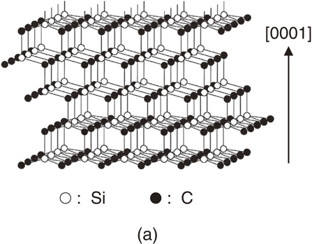
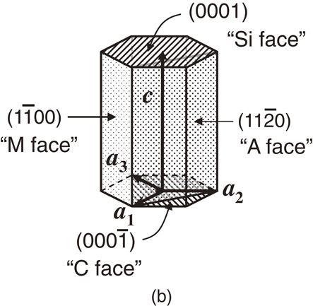
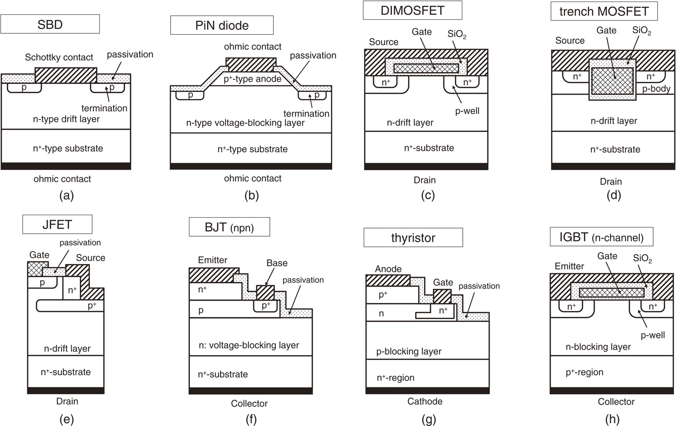
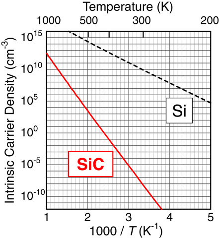
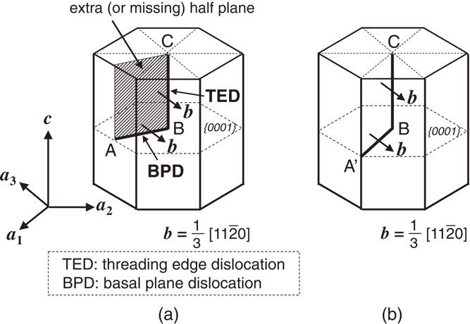
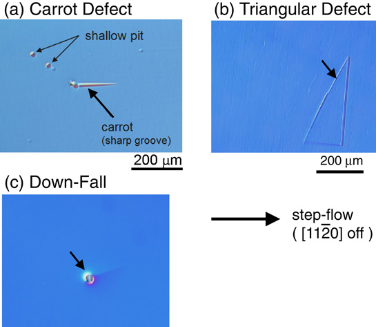
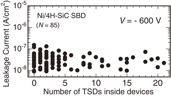
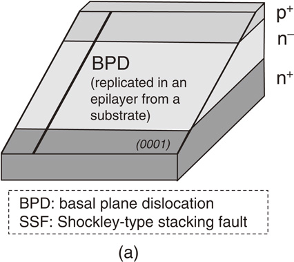
Fig. 40. Correlation between the effective mobility (acceptor density of implanted p-body: 1 × 1017 cm−3) and interface state density integrated from Ec − 0.2 eV to Ec − 0.5 eV (Nit) for SiC(0001),  , and
, and  MOSFETs with nitrided gate oxides. The interface state density was determined by the (a) high (1 MHz)–low method (detection of only slow states) and (b) C–ψS method (detection of both slow and fast states). A nearly one-to-one correlation (slope ∼ −1) is observed when Nit determined from the Dit distribution by the C–ψS method is employed.
Download figure:
Standard image High-resolution image
- (i)The n-channel mobility of SiC MOSFETs is still limited mainly by the very high interface state density, even after the recent process optimization.
- (ii)The channel mobility is affected not only by relatively slow states, which are detected by the conventional high (1 MHz)–low method, but also by very fast interface states, which can be detected by the C–ψS method [and not by the high (1 MHz)–low method].
- (iii)The smaller density of fast interface states for SiC MOS structures on nonpolar faces may be the main reason why higher mobilities can be attained on these faces than on (0001).
In general, SiC MOSFETs exhibit poor subthreshold slopes of 200–500 mV/decade, much larger than the ideal value of approximately 60 mV/decade, at room temperature. The poor subthreshold slope can be reproduced well using the distribution of the interface state density determined by the C–ψS method.12,275)
However, the mechanism of channel conduction in SiC MOSFETs must be much more complicated. The surface roughness of SiC is much larger than that of Si because of the usage of off-axis {0001} wafers and immature surface preparation technology. The roughness scattering may become prominent when the interface state density is further reduced. This is especially important at a high gate bias, at which real MOS devices operate. The influence of the real (not effective) fixed charge on channel mobility has not yet been clarified. Another possible problem is the large fluctuation in surface potential, as revealed by conductance measurements.230,261,276) Since the interface structure of SiC MOS structures can be highly inhomogeneous, the surface potential can fluctuate inside the MOS channel. Thus, the total conduction in the inversion layer may be limited by microscopic regions where the conductivity is greatly suppressed by the fluctuation.
It should be noted that a significant reduction of the interface state density and the improvement of n-channel mobility (120–150 cm2 V−1 s−1) have been achieved on SiC(0001) by "sodium (Na)-contaminated" oxidation.277) An accelerated oxidation rate has been reported for this Na-contaminated oxidation. Another strikingly effective technique to enhance the channel mobility is post-oxidation annealing in POCl3.278) By annealing in POCl3 at 1000 °C for 10 min, a high channel mobility of 89 cm2 V−1 s−1 is attained. The mobility can be further improved to 101 cm2 V−1 s−1 by two-step annealing in POCl3 at 1000 °C and in a forming gas at 700 °C.279) The interface state density and the subthreshold slope for MOSFETs are also significantly improved by the POCl3 annealing. A high channel mobility of 102 cm2 V−1 s−1 has also been attained by boron diffusion into the thermal oxide.280) Although these techniques cannot be employed directly in device manufacturing, it is worth investigating the mechanism of mobility improvement in greater detail in order to acquire important insights into mobility-limiting factors.
10. Conclusions
SiC is a promising wide-bandgap semiconductor for high-voltage and low-loss power devices, and the production of SiC SBDs and power MOSFETs has started. However, the basic understanding of the material and device physics in SiC remains poor. In this paper, the features and present status of SiC power devices were briefly reviewed. Several important aspects associated with the material properties and impurity doping were described. The major extended defects and point defects present in SiC epitaxial wafers were summarized, and our present understanding of the impact of these defects on SiC device performance and reliability was described. Unique features observed in SiC SBDs and power MOSFETs such as the leakage current in SBDs and the mobility-limiting factors in MOSFETs were also reviewed. However, the present paper omitted other important issues such as the implantation-induced damage281–286) and threshold voltage instability of MOSFETs.287–290) The exact mechanism of ohmic behavior at the contact/SiC interface is not very clear.291–296) Furthermore, the switching performance and high-temperature characteristics of SiC power devices were not discussed. For details of these topics, see recent conference proceedings or related books.8,12,13,297–302)
Acknowledgments
The author thanks Professor J. Suda and all the present and former members of his group for their contribution to SiC research. He also acknowledges Professor N. Ohtani of Kwansei Gakuin University and Dr. H. Tsuchida of Central Research Institute of Electric Power Industry for their valuable suggestions on defects in SiC.
Biographies

Tsunenobu Kimoto received the B.E. and M.E. degrees in Electrical Engineering from Kyoto University, Japan, in 1986 and 1988, respectively. He joined Sumitomo Electric Industries, Ltd. in April of 1988, where he conducted research and development of amorphous Si solar cells and semiconducting diamond material. In 1990, he started his academic career as a Research Associate at Kyoto University, and received the Ph.D. degree from Kyoto University in 1996, based on his work on SiC epitaxy, material characterization, and high-voltage diodes. From 1996 to 1997, he was a visiting scientist at Linköping University, Sweden. He is currently a Professor at Department of Electronic Science and Engineering, Kyoto University. His main research activity includes SiC epitaxial growth, optical and electrical characterization, defect electronics, ion implantation, MOS physics, and high-voltage devices. He has also been involved in nano-scale Si, Ge devices and novel materials for nonvolatile memories. He has published over 600 papers in scientific journals and international conference proceedings. He is a member of JSAP, IEEE, MRS, IEICE, and IEE.