
Abstract
Graphene is a two-dimensional material with a one-atom-thick layer of carbon. Since the first report of the excellent electrical properties of graphene in 2004, its unique physical properties have been attracting attention and research on the application of graphene to electronic and photonic devices has been intensively carried out. In this review, recent research trends in the application of graphene to electronic devices, particularly transistors and interconnects, and graphene formation techniques are examined. In addition, the technical issues to be addressed for its application to electronic devices and the prospects for future graphene devices are discussed.
Export citation and abstract BibTeX RIS
1. Introduction
It has been a long time since the limitation of the miniaturization of Si LSIs was first pointed out. Although the time at which the limit will be reached has been gradually postponed, the limit may be reached around 2020 when the channel length of transistors becomes less than 10 nm. Can graphene, the topic of this review, solve this problem? We sometimes hear that the application of graphene to transistors is difficult and that graphene cannot be applied to logic transistors although it may be applied to high-frequency transistors. However, I do not agree with this opinion. I think that graphene has high potential as a future electronic material and that the application of graphene should not be abandoned before our techniques of controlling graphene have matured, although I do not intend to claim that graphene will completely replace Si in electronic devices in the future. It has been just around ten years since graphene was "rediscovered". As explained later, various problems must be solved before graphene can be applied to transistors. The technical advances toward achieving graphene transistors have been remarkable in the last five years. I believe that attractive graphene devices different from Si devices or with functions exceeding those of Si transistors will be realized in the future. In practice, it will take some more time to realize graphene transistors. The application of graphene to transparent electrodes, heat dissipation techniques, and optical devices will probably precede the realization of graphite transistors. The structure of logic transistors using graphene may be different from the currently available MOS structure. Considering these factors, I will briefly introduce the properties of graphene and clarify the current and future challenges by reviewing previous studies, particularly focusing on graphene transistors. Application of graphene to interconnects and the graphene formation techniques required for the realization of various applications are also reviewed. Finally, the prospects for applying graphene to electronic devices are discussed.
2. What is graphene?
Graphene is an ideal two-dimensional one-atom-thick honeycomb lattice made of carbon atoms. The atomic structure of graphene is shown in Fig. 1. Graphene is a one-atom-thick layer of graphite as a layered material and its existence has been theoretically known for many years;1–3) however, a one-atom-thick layer of graphene has been considered to be thermodynamically unstable.4,5) Novoselov et al. experimentally identified graphene as a one-atom-thick layer for the first time (which is not necessarily contradictory to the theory because the layer was supported by a substrate).6) They experimentally demonstrated its high mobility while examining its electrical properties. This study,6) along with studies on the unique quantum Hall effect published the following year,7,8) and the fact that graphene is easily prepared using adhesive tape, triggered a boom in graphene research in subsequent years.

Fig. 1. Schematic of atomic structure of graphene.
Download figure:
Standard image High-resolution imageGraphene has excellent properties, such as a high mobility (approximately 100,000 cm2 V−1 s−1 at room temperature), durability at a high current density (109 A/cm2), good mechanical properties, and high thermal conductivity. The unique electronic state of graphene results in its excellent electrical properties. Figure 2 shows a three-dimensional plot of the energy band dispersion of graphene. The existence of K and K' points where the dispersion relationship is conical, with the energy being proportional to the wave number around the Fermi energy, is characteristic of graphene. This electronic state originates from the existence of two nonequivalent carbon atoms in a unit cell. Details of the electronic state of graphene are not explained here (refer to Ref. 9). This electronic state induces various characteristic phenomena, such as the suppression of backscattering10–12) and Klein tunneling.13,14) In this review, however, electrical properties from the viewpoint of its application to electronic devices, rather than the physical aspects of graphene, are mainly discussed.

Fig. 2. Three-dimensional plot of the energy band structure of graphene.
Download figure:
Standard image High-resolution image3. Electrical properties of graphene
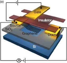
Graphene is a zero-gap semiconductor with a high electrical conductance. However, unlike general metals, the current can be modulated by gate biasing. Figure 3 shows a scanning electron microscopy (SEM) image of the first back-gate transistor with a graphene channel demonstrated by Novoselov et al.6) The key to facilitating the observation of monolayer graphene was to place the graphene layer on a SiO2 layer, which can be observed using an optical microscope.15) The mobility of the graphene channel was approximately 10,000 cm2 V−1 s−1. This value is not particularly high compared with that of compound semiconductors; however, it is surprising considering that this value was obtained for a device made from common graphite crystals using ordinary adhesive tape. Graphene is also very attractive as a semiconductor material because of its equal hole and electron mobilities.

Download figure:
Standard image High-resolution image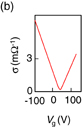
Fig. 3. (a) SEM image of a graphene device fabricated by Novoselov et al.6) © 2004 AAAS. (b) Dependence of conductance (σ) on back-gate voltage (Vg), reproduced by referring to Ref. 6.
Download figure:
Standard image High-resolution imageThere have been a number of reports on the factors that affect the mobility of graphene. Thus far, scattering of carriers by charged impurities originated from the SiO2 substrate,16–18) scattering by the acoustic phonon of graphene itself,19,20) and scattering by polar optical phonons of the substrate19,21) have been pointed out as such factors. Hwang et al. theoretically predicted that a mobility of approximately 2,000,000 cm2/V can be achieved by suppressing the amount of charged impurities.17) Chen et al. demonstrated that 1) the room-temperature mobility of graphene is suppressed to approximately 40,000 cm2 V−1 s−1 by the effect of polar optical phonons of SiO2 and 2) the room-temperature mobility is approximately 200,000 cm2 V−1 s−1 when only acoustic phonons of graphene, not SiO2, affect the mobility (at a carrier density of approximately 1012 cm−2 for both cases).19) The results of this study indicate that the type of substrate significantly affects the mobility of graphene. Bolotin et al. fabricated a device in which a graphene channel was suspended to remove the effects of the substrate. Mobilities of 200,000 cm2 V−1 s−1 at liquid helium temperature and 120,000 cm2 V−1 s−1 at 120 K were obtained at a relatively low carrier density of 2 × 1011 cm−2.22) After that, Mayorov et al. demonstrated that 1) a mobility of 1,000,000 cm2 V−1 s−1 can be obtained at low temperatures and 2) the mobility decreases to 20,000–30,000 cm2 V−1 s−1 at about room temperature because of flexural phonons.23) Dean et al. fabricated graphene transistors on a hexagonal boron nitride (h-BN) flake, which have an atomically smooth surface and a higher optical phonon energy than graphene. A mobility of 140,000 cm2 V−1 s−1 was obtained near the charge neutrality point at room temperature, and a mobility of approximately 25,000 cm2 V−1 s−1 was obtained at a high carrier density.24) From their results, the improvement in mobility is considered to be caused mainly by decrease in charged impurities, which was also supported by Kelvin probe force microscopy results.25)
As explained above, the effects of disturbance factors, such as charged impurities and the phonons in substrates, should be suppressed to bring out the inherent electrical properties of graphene. Although many papers have reported that the density of charged impurity residues caused by device-fabrication processes can be decreased by annealing,22,26) optimization appropriate for each process may be necessary. The above-mentioned h-BN substrates can be used to suppress the effects of substrates; however, a technique for synthesizing high-quality large-area h-BN substrates has not yet been established. Developing such a technique as well as investigating other materials will be necessary in the future.
The high mobility of graphene is certainly attractive. However, the on–off current ratio of transistors with a graphene channel is only approximately 10 because there is no bandgap in graphene (Fig. 3). Increasing the on–off current ratio will be essential to apply graphene to transistors, and the formation of a bandgap in graphene has been attempted. The details are explained in the next section.
4. Control of bandgap of graphene
There have been many reports on the formation of a bandgap in graphene. The methods used include the formation of graphene nanoribbons (GNRs), the application of an electric field to bilayer graphene, and the modification of graphene. These methods are explained sequentially in this section.
4.1. Formation of GNRs
Japanese scientists had already reported the electronic states of GNRs before graphene attracted its current attention.27,28) The results of tight-binding calculations showed that GNRs with armchair-shaped edges have a bandgap under certain conditions, whereas in GNRs with zigzag-shaped edges, the edge states appear at the Fermi level, in which the charge density strongly localized on the zigzag edge sites. Graphene with armchair edges behaves as a metal when the number of dimer lines is Na = 3p − 1, where p is an integer (Fig. 4). The ratio of GNRs with metallic behavior is 1/3, which is equal to that for carbon nanotubes (CNTs). Son et al. demonstrated that GNRs have a bandgap regardless of the edge termination (armchair or zigzag) by performing a first-principles calculation [local density approximation (LDA)].29) The bandgap and its dependence on the ribbon width differ with the type of edge termination and Na (the case of GNRs with armchair-shaped edges is shown in Fig. 5). Yang et al. demonstrated that the bandgap is estimated to be larger when the effects of the electron–electron interaction are taken into consideration using a first-principles many-electron Green's function approach within the GW approximation (Fig. 5).30)

Fig. 4. Schematic of GNR with armchair edges. Na is the number of dimer lines.
Download figure:
Standard image High-resolution image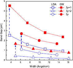
Fig. 5. Bandgap for GNRs with armchair edges obtained by first-principles calculations [LDA and many-body perturbation theory (GW approximation)].30) There are three series of GNRs with Na = 3p, 3p + 1, and 3p + 2. © 2007 American Physical Society.
Download figure:
Standard image High-resolution imageGNRs have been experimentally fabricated by a top-down approach using electron beam lithography and oxygen plasma etching.31–33) Han et al. fabricated GNRs with a width of down to 14 nm and demonstrated that the energy gap, Eg, is expressed as a function of the ribbon width as

where α = 2 eV and W* = 16 nm (Fig. 6).33) W* is the inactive edge width and is interpreted as the difference between the apparent ribbon width and the actual ribbon width or the decrease in the effective ribbon width as a result of edge defects. Research on the electron transport in GNRs fabricated by a top-down approach has since continued, and the above energy gap is now interpreted as a transport gap, which is generally larger than the theoretically calculated bandgap.34,35) The transport gap has been interpreted using various models including Anderson localization, variable-range hopping, and the Coulomb blockade model. In all models, the existence of defects at the edges causes the transport gap. Thus far, GNRs with ideal edges have not been successfully fabricated by any top-down approach. Further improvement in lithography and etching techniques will be required.
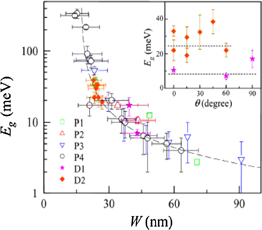
Fig. 6. Dependence of energy gap (Eg) on ribbon width (W) reported by Han et al.33) The insert shows that Eg is independent of the relative angle (θ) of GNR. © 2007 American Physical Society.
Download figure:
Standard image High-resolution imageOther methods have also been used in attempts to form GNRs. For example, Li et al. formed GNRs by heating expandable graphite at 1,000 °C in a forming gas, dispersing the resulting graphite in a 1,2-dichloroethane (DCE) solution of poly(m-phenylenevinylene-co-2,5-dioctoxy-p-phenylenevinylene) (PmPV), and ultrasonicating the solution.36) GNRs with a width ≤10 nm were obtained. Transmission electron microscopy (TEM) revealed that these GNRs had ultrasmooth edges. Regarding the electrical properties, an on–off current ratio of 105–107 was obtained for the GNRs with a width <10 nm at room temperature, which was a significant advance considering that the maximum on–off current ratio of the GNRs fabricated by a top-down approach was only 10–100. Similarly, a mobility of 100–200 cm2 V−1 s−1 was obtained for the GNRs. This combination of the on–off current ratio (105–107) and mobility (100–200 cm2 V−1 s−1) is the best reported combination for GNRs, to the best of my knowledge. The bandgap was also in reasonable agreement with that obtained by first-principles calculation (without consideration of the many-body effect). With this method, relatively high-quality GNRs can be obtained; however, the control of the ribbon width is difficult.
Methods of fabricating GNRs from CNTs have also been proposed.37,38) In one method, GNRs were fabricated by cutting the side walls of multiwalled CNTs in the lengthwise direction with the treatment of multiwalled CNTs with a strong oxidant.38) Here, the obtained GNRs were graphene oxide; they had poor electrical properties and required reduction treatment for use as graphene. After this method was proposed, another method of fabricating GNRs by mildly oxidizing multiwalled CNTs in a gas phase and dispersing the resulting multiwalled CNTs in a DCE solution of PmPV was reported.39) The obtained GNRs had smooth edges. A high mobility of 1,500 cm2 V−1 s−1 was obtained for the GNRs with a width of 14 nm. The above methods of fabricating GNRs from CNTs have been successful only for relatively thick multiwalled CNTs and only relatively wide GNRs have been obtained.
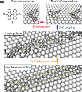
As a true bottom-up approach, a method of fabricating GNRs with a uniform width from anthracene dimers as a precursor was reported in 2010.40) Figure 7 shows the fabrication method. First, anthracene dimers with both ends terminated with Br are deposited on Au substrate. When the substrate temperature is increased to 200 °C, debromination occurs and the sites from which Br atoms have been removed bond with each other. When the temperature is further increased to 400 °C, cyclodehydrogenation occurs to form GNRs. As shown in Fig. 7(b), the ribbon width is well controlled and a Raman vibration mode that depends on the ribbon width is observed. According to the representation in Fig. 4, the fabricated GNRs are those with armchair-shaped edges with N = 7, and the bandgap is approximately 3.7 eV (Fig. 5). Ruffieux et al. estimated the bandgap by scanning tunneling microscopy (STM) to be approximately 2.7 eV,41) in reasonable agreement with the theoretical bandgap considering the mirror charge effect of the Au substrate. The electrical properties of GNRs were measured by STM and insulating behavior was obtained as expected.42)
Download figure:
Standard image High-resolution image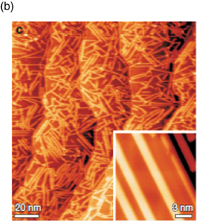
Fig. 7. (a) Schematic of GNR fabrication by bottom-up approach and (b) STM images of fabricated GNRs.40) © 2010 Macmillan Publishers Ltd.
Download figure:
Standard image High-resolution imageThe bandgap of 3.7 eV may be too large for the application of GNRs to transistors. More recently, the fabrication of GNRs with larger widths has been reported.43) It is expected that the bandgap will be freely controlled in the future.
4.2. Use of bilayer graphene
Another method of forming a bandgap in graphene is to apply an electric field perpendicularly to an AB-stacked bilayer graphene (Fig. 8). The formation of a bandgap in graphene by this method was first predicted by theoretical calculations.44,45) The essence of this method is to place two types of carbon atom (A- and B-site carbons) in different environments, which is realized by applying an electric field perpendicularly to the bilayer graphene. Theoretically, the formation of a bandgap of 200–300 meV is considered to be possible by applying a displacement field of approximately 1 V/nm.46)
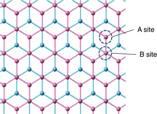
Fig. 8. Top view of AB-stacked bilayer graphene.
Download figure:
Standard image High-resolution imageBandgap formation was first observed in bilayer graphene formed on a SiC substrate without the application of an electric field.47) This is because the SiC-side layer in the bilayer graphene on the SiC substrate is electron-doped, resulting in an inequality in the charge density (potential) between the two layers. Afterward, Oostinga et al. experimentally demonstrated that a bandgap can be formed by applying an electric field between electrodes placed above and below a bilayer graphene channel.48) However, the bandgap estimated from the electrical properties was no more than 10 meV and the effects of defects on the energy level within the bandgap were pointed out. Zhang et al. optically estimated the bandgap by infrared microspectroscopy and obtained a bandgap of approximately 250 meV for a displacement field of approximately 3 V/nm.49) In this case, however, the energy gap obtained from the electrical properties was much smaller than 250 meV. A research group of IBM Corporation obtained an on–off current ratio of approximately 100 at room temperature by applying a displacement field of approximately 2.2 V/nm. Researchers estimated a bandgap of approximately 130 meV from the temperature dependence of the on–off current ratio.50) This is the highest-level bandgap obtained from electrical properties.
The application of an electric field, as explained above, not only requires complicated device structures but also poses a risk of dielectric breakdown. As an alternative method, the formation of a bandgap by the molecular doping of bilayer graphene has been attempted.51–54) Park et al. transferred a bilayer graphene onto a self-assembled monolayer (SAM) serving as an n-dopant, on which tetrafluoro-tetrafluorotetracyano-quinodimethane (F4-TCNQ) was deposited as a p-dopant.54) The on–off current ratio was approximately 25 at room temperature, which was much lower than expected and may have been affected by the energy levels due to defects. This method is possibly promising compared with the method of actually applying an electric field, because a relatively large effective electric field can be applied to the bilayer graphene if appropriate molecular materials for doping are selected. Theoretically, the formation of a bandgap exceeding 300 meV is expected.55)
4.3. Formation of bandgap in graphene by other methods
It was explained above that the essence of bandgap formation in bilayer graphene is to place two types of carbon atom (A- and B-site carbons) in different environments. This has also been realized by methods other than those explained above. A report showed that, theoretically, a bandgap is formed in a lattice-matched graphene sheet on a BN substrate.56) The experimental formation of a bandgap in graphene epitaxially grown on a SiC substrate57) and graphene grown on a MgO substrate58) has been reported.
The formation of a bandgap by producing arrays of holes has also been reported.59,60) The distance between holes, i.e., the neck width, plays a similar role to the ribbon width in the formation of a transport gap. The transport properties depend on minute differences in the hole shape, as has been theoretically calculated.61) The control of the edge shape is also important in this method.
The formation of a bandgap by modifying the graphene surface with heteroatoms has also been reported. Examples of modified surfaces include graphene oxide,62,63) graphene fluoride,64–66) and hydrogenated graphene,67–69) which are basically insulators. Partial modification and the formation of pseudo-GNRs (called nanoroads)70) by modifying the surrounding atoms instead of etching have been proposed. We recently reported the formation of a transport gap by irradiating the graphene with a helium ion beam to embed low-density defects in the graphene lattice,71) which is a slightly different from the modification above. The graphene obtained by these modification methods has a high on–off current ratio; however, finding a balance between the on–off current ratio and the mobility remains a challenge.
4.4. Issues to be resolved in bandgap formation
A bandgap can be formed in graphene by the methods discussed above. However, graphene with both a bandgap and high mobility has not been realized. The reason behind this is the trade-off relationship between bandgap formation and high mobility (Fig. 9).72–74) In addition, insufficient control of the edges of GNRs and the interface of bilayer graphene is considered to be a major cause of low mobility. For example, a GNR with an ideal edge is considered to have mobility (experimentally, approximately 100,000 cm2 V−1 s−1 75)) and device performance comparable to those achieved by CNTs. In fact, performances equivalent to those of CNTs or superior to those of Si were predicted in the simulation of transistors using ideal GNRs.76–78)
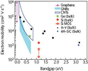
Fig. 9. Relationship between bandgap and mobility plotted by Schwierz.74) The results for CNTs and GNRs were obtained by simulations. © 2010 Macmillan Publishers Ltd.
Download figure:
Standard image High-resolution image5. Device technologies required for transistor fabrication
5.1. Techniques of depositing gate-insulator and passivation films
For the application of graphene to devices, an insulating passivation film or a gate-insulator film should be deposited on a graphene layer. However, graphene is a material with a one-atom-thick layer of carbon and the deposition may damage the graphene or change its properties. In this section, techniques related to the deposition of a passivation film on a graphene layer are described.
Lemme et al.79) fabricated a back-gate transistor using exfoliated graphene, and then made a top gate with a vapor-deposited SiO2 film as a top-gate insulator. The mobility of the back-gate transistor was approximately 5,000 cm2 V−1 s−1; however, it significantly decreased to 500–700 cm2 V−1 s−1 upon the deposition of the insulating film. Wu et al. fabricated a top-gate transistor by physically depositing (maybe vapor depositing) SiO2 on graphene formed on a SiC substrate.80) The mobility was as high as 5,400 cm2 V−1 s−1, in contrast with the low mobility above. In general, a SiO2 film deposited on a graphene layer tends to cause little damage to graphene, although it may depend on deposition conditions.
Growing a high-dielectric-constant (high-k) film on a graphene layer has been attempted by atomic layer deposition (ALD). The deposition of a high-k film on a graphene layer by ALD is difficult because the surface of graphene is stable and hydrophobic. Xuan et al.81) and Wang et al.82) showed that HfO2 or Al2O3 preferentially grows on the edges and defect sites of graphene by ALD. Before their reports, Williams et al. demonstrated that an Al2O3 film can be uniformly deposited by ALD when a noncovalent functionalization layer (NCFL) consisting of NO2 and trimethylaluminium (TMA) was deposited on graphene in advance.83) The mobility of graphene after deposition of an insulating film was approximately 7,000 cm2 V−1 s−1, indicating that the properties of graphene did not deteriorate. Thus, a hydrophilic seeding layer is generally required for ALD. For example, Wang et al. demonstrated that an Al2O3 film was uniformly deposited on graphene by pretreating graphene with a 3,4,9,10-perylene tetracarboxylic acid (PTCA) solution.82) Kim et al. reported that uniform and damage-free deposition of an Al2O3 film by ALD is possible by preliminarily depositing and oxidizing Al film with a thickness of 1–2 nm by electron-beam vacuum evaporation. They also reported that the mobility of the exfoliated graphene after the deposition of the Al2O3 film was approximately 8,000 cm2 V−1 s−1.84) Before the report by Kim et al., Miyazaki et al. reported that an Al2O3 film is effective as a gate insulator.85) Farmer et al. reported that a HfO2 film can be formed without a decrease in mobility using a low-dielectric-constant polymer layer (JSR Micro NFC 1400-3CP) as a buffer layer.86) However, the dielectric constant of the polymer layer is as low as 2.4 and requires improvement to enhance the device performance. The ALD of Al2O3 and HfO2 using a monolayer of perylene-3,4,9,10-tetracarboxylic dianhydride (PTCDA) as a seeding layer has been reported.87) More recently, an h-BN film was synthesized by chemical vapor deposition (CVD) and transferred to a target substrate for use as a gate-insulator film.88)
As explained above, methods of depositing insulating films that suppress the damage to graphene have been gradually established. However, decreasing the effective oxide film thickness (EOT) is a future challenge because a buffer layer is currently required to deposit a material with a high dielectric constant.
5.2. Contact resistance
Various experimental studies have been carried out on metal/graphene interfaces.89–100) The contact resistance has been reported to depend on the type of metal; however, the direct comparison of results reported in these studies is difficult: The graphene surfaces in these studies were covered with a layer of photoresist residues because electrodes were formed by lithography,26,98,101) which may obscure the differences in the intrinsic properties of metals. Therefore, the charge transfer between graphene and a metal owing to a difference in the work function between them, which has been theoretically predicted,102,103) has not been precisely experimentally reproduced.94,97,98) The charge transfer from a metal to graphene appears to occur since electron–hole asymmetry is often observed for the back-gate-voltage dependence of a drain current.91,100,104) In addition, the contact resistance has been experimentally confirmed to vary as a function of the back-gate voltage.89,94)
Xia et al. used Pd as an electrode and experimentally and theoretically determined the contact resistance in a Pd-graphene junction to be approximately 110 Ω µm.100) According to Landauer's approach, which they used, the contact conductance (G) of the graphene-metal junction can be expressed as G = (4e2/h)TM, where M is the number of conduction modes in the graphene, T is the carrier transmission probability, e is the elementary charge, and h is Planck's constant. M can be increased by changing the Fermi level of graphene, i.e., by electrostatic doping and charge transfer from the electrode metal to graphene. However, the behavior of T is complicated because T depends on various factors, such as the metal/graphene coupling strength and the mean free path of electrons in the graphene below the metal. According to Xia et al., the contact resistance decreases with increasing quality of the graphene, namely, increasing mean free path.
Nagashio and co-workers92,93) demonstrated that the density of states of graphene underneath a Au electrode is increased by applying back-gate bias, and they obtained a contact resistance of approximately 50 Ω µm. In contrast, when the graphene surface is contaminated with resist residues, the density of states of graphene underneath Ni electrode is modulated, whereas for a clean graphene surface obtained by a resist-free process, no modulation occurs. In addition, the contact resistance in the latter case was higher than that in the former case. This is considered to be due to the interaction between the π-electrons in graphene and the d-electrons in Ni. From the results obtained by Nagashio and co-workers, keys to decreasing contact resistance are 1) to maintain the electronic state of graphene and increase the density of states of graphene underneath a metal layer using a metal that weakly interacts with graphene and 2) to increase the transmission probability of electrons by reducing the resist-residue contamination on graphene to shorten the distance between the metal and graphene. Their electrostatic doping by applying back-gate bias cannot be adopted for general top-gate transistor geometries and some modifications will be required.
5.3. Doping
There are two doping methods that can be used for graphene: substitutional doping and chemical doping (or surface transfer doping).105) In typical n-type substitutional doping, N atoms are substitutionally doped into graphene to replace carbon atoms. Concretely, the following methods have been reported: mixing ammonia into methane during graphene synthesis,106) the exposure of graphene to ammonia plasma,107) and nitrogen or ammonia annealing after the N+-ion irradiation of graphene samples.108) For p-type substitutional doping with B atoms, CVD using methane and diborane was recently reported.109) However, controlling the carrier concentration while maintaining the original properties of the graphene is difficult because the substitutional doping significantly alters the electronic states of graphene.110)
Chemical doping in which molecules are adsorbed on the surface of graphene to induce electron transfer has been attempted. The use of poly(ethylene imine) (PEI) as an n-type dopant111) and doping using NH2-terminated SAMs112) have been attempted. The doping level using NH2-terminated SAMs was approximately 8 × 1012 cm−2. As p-type dopants, the use of NO2 molecules,113,114) F4-TCNQ,115) and diazonium salts111) has been reported. It was estimated that a doping level of approximately 3 × 1013 cm−2 is realized by the adsorption of various types of n- or p-type dopant molecules.116) Unlike substitutional doping, chemical doping does not directly modulate the electronic states; however, nonuniform deposition, which can induce charged impurities, may degrade the mobility of graphene, which requires attention.
6. Graphene formation techniques
Exfoliating a monolayer of graphene from graphite is an ideal method of obtaining graphene to study its properties. However, for the application of graphene to industrial use, the development of techniques to form uniform large-area graphene films is essential. Methods of forming graphene that have recently attracted attention as research targets include the annealing of a SiC substrate surface117–121) and CVD. In 1975, graphene was first formed on a SiC substrate in high vacuum by heating the SiC.121) Since then, several prominent papers, such as those on the first evaluation of the electrical properties of graphene,117) determination of the number of layers by low-energy electron microscopy (LEEM),119) improving the surface roughness and the uniformity of the number of graphene layers formed by annealing in an Ar atmosphere,118) and the formation of quasi-free-standing graphene,120) have been published. Because of space limitations, details of these methods are not discussed here. The formation of graphene by CVD is reviewed below.
In CVD, graphene films are generally synthesized on a substrate with a thin catalyst film, such as Cu, Ni, or Co film, or on a metal catalyst foil by heating the substrate or the foil and introducing a hydrocarbon gas.122–126) CVD is an effective method for application to electronic devices because it can be easily used with large-area substrates and is a versatile semiconductor process.
Attempts to form graphene by CVD started with the formation of graphene on polycrystalline Ni films/foils.122,125,126) The formation of graphene on Ni films is considered to be due to the precipitation of solid-solution carbon because of a high solubility of carbon in Ni. When catalysts with a high solubility of carbon, such as Ni and Co, are used, multilayer graphene is generally formed. Controlling the number of layers is difficult owing to the variation in the amount of carbon deposited among different grains of polycrystalline films. Our group attempted to form graphene on Fe films and obtained similar results.123,127) To obtain a graphene monolayer, a Cu catalyst is superior in terms of controlling the number of layers, as reported in 2009, and enables the synthesis of a graphene monolayer over the entire substrate.124) The formation of graphene on Cu is understood to be a result of a catalytic reaction of hydrocarbons because of the low solubility of carbon in Cu.128) Recently, graphene having grains of millimeter-order size has been formed on Cu foils (Fig. 10).129–131) Methane gas was used as the carbon source. The methane partial pressure as well as the amount of hydrogen were found to significantly affect the formation of graphene.131,132) Similar graphene monolayers can be synthesized on a Cu film on a Si substrate, in addition to on a Cu foil alone. Our group has recently succeeded in synthesizing graphene on a 300-mm-diameter Si wafer (Fig. 11).133)
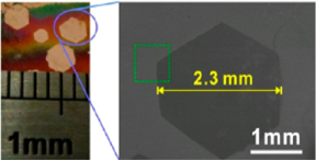
Fig. 10. Optical microscopic image (left) and SEM image (right) of single-crystal graphene idlands formed on Cu foils.131) © 2012 American Chemical Society.
Download figure:
Standard image High-resolution image
Download figure:
Standard image High-resolution image
Fig. 11. (a) 300 mm Cu/SiO2/Si wafer on which graphene was formed.133) (b) Raman spectra obtained at points A–E in (a).
Download figure:
Standard image High-resolution imageThe catalysts used in the above experiments were polycrystalline and the formed graphene was also polycrystalline over the entire substrate, although the grain size differed. Recently, epitaxial monolayer graphene of centimeter-order size has been formed using epitaxial catalysts, such as Co and Cu.134–136) The evaluation of whether the obtained graphene is truly single crystals or not is difficult; however, these studies provide a direction for developing methods of forming single-crystal graphene.
As explained above, the techniques used to form graphene over an entire substrate while controlling the grain size are making rapid progress these days. Mobility of up to approximately 25,000 cm2 V−1 s−1 has been obtained at room temperature,137) which is equivalent to that of an exfoliated monolayer of graphene. From the viewpoint of applying graphene to transistors, the formation of GNRs by CVD using a bottom-up approach is desirable. Our group has recently found that GNRs can be grown selectively at the narrow twin crystal regions formed when Cu films are annealed.138) A recent report showed that GNR was formed by MBE, instead of CVD, using a vicinal SiC substrate as a template.139) I hope that further technical developments will be made in this field in the future.
Because graphene is formed on metal catalyst foils by CVD, as discussed above, a transfer process is generally required to fabricate graphene transistors. Several research groups including our group have reported the transfer-free fabrication of transistors.123,140) The challenge is to form graphene directly on an insulating substrate. Although several attemps have been reported,141,142) the quality of the formed graphene has generally been low. Future developments in this field are also expected.
7. Application of graphene to transistors operating at high frequencies
The application of graphene to devices operating at high frequencies has been mainly reported by researchers of IBM Corporation.143–148) Table I summarizes the history of their achievements reported. The cutoff frequency (fT) was as low as 26 GHz in 2009144) but had increased approximately tenfold by 2012.145) As shown in Table I, fT did not necessarily increase in inverse proportion to the gate length at the beginning; however, fT was inversely proportional to the gate length in the 2012 report. This improvement is due to various factors, including the control of the quality and interface of graphene, and the reduction in contact resistance. According to their reports, the values of fT and the gate length of the graphene formed by CVD were equivalent to those for the graphene synthesized on SiC. It is noteworthy that the properties of transistors with CVD graphene were improved when fabricated on diamond-like carbon (DLC) film,146) because of the high energy of its optical phonons compared with that of SiO2. To the best of my knowledge, the highest fT of 427 GHz was reported by a research group at University of California, Los Angeles (UCLA).149) Their method is distinctive in that arrays of gate stacks were fabricated separately and then transferred onto a substrate with graphene on top, on which the source and drain electrodes were formed by a self-aligned process. An fT of 427 GHz was obtained for an exfoliated monolayer of graphene, and fT for the graphene formed by CVD was 212 GHz, which is close to that reported by the research group of IBM.
Table I. History of properties of high-frequency transistors reported by research groups of IBM.
| Reference | fT (GHz) | Gate length (nm) | Graphene | Gate-insulator |
|---|---|---|---|---|
| 144 | 26 | 150 | From graphite | NO2 + ALD-Al2O3 (12 nm) |
| 148 | 50 | 350 | From graphite | Naturally oxidized Al2O3 (2 nm) + ALD-Al2O3 (12 nm) |
| 143 | 100 | 240 | On SiC | NFC (10 nm)/HfO2 (10 nm) |
| 147 | 170 | 90 | On SiC | NFC (10 nm)/HfO2 (10 nm) |
| 146 | 155 | 40 | CVD on DLC | Naturally oxidized Al2O3 (10 nm) + ALD-Al2O3 (15 nm) |
| 145 | 300 | 40 | CVD on DLC | Naturally oxidized Al2O3 (? nm) + ALD-Al2O3 (10 nm) |
| 145 | 350 | 40 | On SiC | Si3N4 (10 nm) |
Figure 12 shows the relationship between fT and the gate length for various semiconductor materials including graphene. Values of fT for compound semiconductors are still superior to that of graphene, although fT for graphene is approaching the best value for compound semiconductors. Theoretically, fT exceeding 1 THz has been predicted for graphene.150) To realize this value, decreases in the contact resistance and EOT are essential. Although higher values of fT have gradually been obtained, the maximum oscillation frequency (fmax) reported by the research groups of IBM was only 40 GHz, which is one order of magnitude smaller than that of compound semiconductors. The reason behind this is the inability to decrease the drain conductance (gds) because of the poor saturation properties. A method of decreasing the apparent gds was proposed,151) but it is still unsatisfactory. To improve the saturation properties, the formation of a bandgap is naturally the final goal.

Fig. 12. Relationship between cutoff frequency (fT) and gate length of various semiconductor materials including graphene.
Download figure:
Standard image High-resolution imageFor the application of graphene to devices operated at high frequencies, the use of the ambipolar properties of graphene has been proposed. Our group proposed an inverter and a one-transistor binary digital phase modulator with both a top gate and a back gate.152) Wang et al. proposed frequency doublers.153) The application of graphene to these kinds of devices utilizing its unique properties is expected to expand in the future.
8. Graphene for interconnect applications
In this review, the application of graphene to transistors has mainly been discussed. In this section, I will briefly explain the application of graphene to interconnects. Along with the miniaturization of devices, LSI interconnects are facing two problems: decreased reliability and increased effective resistivity of Cu interconnects. According to the International Technology Roadmap for Semiconductors 2011, the resistivity of Cu interconnects is estimated to exceed 10 µΩ cm (1.7 µΩ cm for bulk Cu) by about 2020 when the linewidth is expected to have become smaller than 10 nm. Therefore, CNTs and graphene have been attracting attention as new interconnect materials.
It was reported that the reliability of graphene interconnects, as well as CNT interconnects, is superior to that of Cu interconnects. The breakdown current densities of both an exfoliated monolayer of graphene and CVD graphene are of the order of 108–109 A/cm2.154,155) Figure 13 shows the results of a reliability test conducted by our group.156) The current density durability of the CVD graphene is superior to that of Cu.
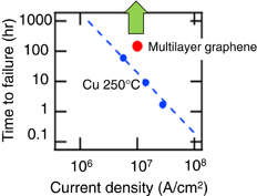
Fig. 13. Time to failure when high current density is applied to multilayer graphene interconnects (red circle) and Cu interconnects (blue circles). The graphene interconnects did not break when a current density of 107 A/cm2 was applied for 150 h.156)
Download figure:
Standard image High-resolution imageHowever, graphene interconnects having lower resistance than that of Cu interconnects have not been reported and the development of such graphene interconnects is a current challenge. The resistivity of bulk graphite is about 40 µΩ cm, which is one order of magnitude higher than that of Cu (1.7 µΩ cm). Interconnects with a low resistivity cannot be obtained simply by patterning graphene.157,158) One method of reducing resistivity is to use the ballistic conduction of GNRs, similarly to the case of CNTs. The resistivity of GNR interconnects was first estimated by simulation.159,160) Although the simulation results vary depending on the assumptions, for linewidths smaller than 10 nm, the resistivity of graphene becomes lower than that of Cu owing to the increase in the effective resistivity of Cu.160) Note that this result is greatly affected by the state of edge termination.159) The complete specular reflection of electrons at the edges is ideal; however, it is very difficult to obtain ideal edges by a top-down approach.
Intercalation is another method of reducing the resistivity of graphene. Lowering the resistivity of graphene by intercalation was first reported many years ago.161) Some materials have been reported to achieve resistivity lower than that of Cu by intercalation to graphite. Xu et al. demonstrated by simulation that AsF5-doped multilayer GNRs can have lower resistivity than that of Cu.159) Murali experimentally demonstrated that an electrostatically doped exfoliated GNR monolayer can have a resistivity comparable to that of Cu. Our group obtained a resistivity of 4.1 µΩ cm, which is equivalent to that of Cu, by the intercalation of FeCl3 in CVD graphene interconnects.162) This value was obtained for graphene interconnects with a width of several microns. It is necessary to examine the feasibility of obtaining resistivity lower than that of Cu for much narrower interconnects.
9. Graphene devices based on new concepts
Recently, there has been a move to develop graphene switching devices based on new concepts because the formation of a bandgap in graphene is still difficult, as explained earlier. This new trend is explained in this section.
Yang et al. fabricated a device with a heterojunction between graphene and hydrogen-terminated Si (Fig. 14).163) Switching operation was realized by changing the Schottky barrier height through the adjustment of the gate voltage to control the Fermi level of graphene. They called this device a graphene "barristor" and obtained an on–off current ratio of approximately 105. However, this device has some drawbacks, such as a relatively small on-current and the difficulty of obtaining saturation characteristics, as observed in general transistors, with increasing bias current.
Download figure:
Standard image High-resolution image
Fig. 14. (a) Schematic of graphene barristor and (b) SEM image of graphene barristor before formation of top gate.163) © 2012 AAAS.
Download figure:
Standard image High-resolution image
Britnell et al. fabricated tunneling transistors with two graphene layers sandwiching either BN or MoS2.164) Here, the tunneling current could be modulated by changing the Fermi energy of the two graphene layers through the adjustment of the back-gate voltage. Vaziri et al. fabricated graphene-based hot electron transistors.165) The tunneling current was controlled by changing the potential applied to the graphene, although details are not given here for space limitation. An on–off current ratio exceeding 104 was obtained for these devices, but there was a problem of a small on-current.
Banerjee et al. proposed a device called a bilayer pseudospin field-effect transistor (BiSFET) that was based on a completely new concept.166,167) In this device, a thin insulating film is sandwiched between two graphene layers. When the electron concentration in one graphene layer and the hole concentration in another graphene layer are balanced at a high concentration, the Bose condensation of electron–hole pairs (excitons) is induced to markedly decrease the tunneling resistance, allowing current to flow. They reported that the power consumption per clock cycle of this device is much smaller than that of currently available metal–oxide–semiconductor field-effect transistors (MOSFETs). The device is very attractive as it is based on a new concept, although they recognized some issues to be addressed in their theory.
As explained above, new devices based on new concepts have been proposed. The key to the realization of future devices will be to utilize the unique characteristics of graphene and graphene heterojunctions with other two-dimensional materials.
10. Final remarks
In this review, research on graphene transistors has mainly been discussed. Graphene has excellent electrical properties, and a bandgap can be created by, for example, forming GNRs; however, these potential properties of graphene have not been fully brought out. This is mainly due to the insufficient control of interfaces and edges. To solve these problems, techniques for the heteroepitaxial growth of other two-dimensional materials, such as h-BN, may be necessary. Considering the recent rapid advances in technology, the control of interfaces and edges is expected to be possible in the near future.
The use of conventional miniaturization technologies to improve the performance of semiconductor devices is predicted to reach its limit in the near future. Although the use of graphene will not necessarily advance the miniaturization of semiconductor devices, graphene is expected to be used as a material for "More Moore" high-end logic channels with a higher speed and lower power consumption at the same dimensions. Its application to tunneling transistors is also expected. From the viewpoint of the "More than Moore" approach, the combination of high-frequency or optical devices using graphene with Si devices is expected, which would be less difficult and realized before "More Moore" devices. Now that the realization of graphene with a low resistivity is being reached, the application of graphene to LSI interconnects and flexible/transparent interconnects is also promising.
In the previous section, I introduced a layered device consisting of graphene and other two-dimensional materials that operates on the basis of a new concept. For the realization of new properties of graphene and their application, the combination of graphene with other two-dimensional materials and topological insulators will play a key role; this is an area of research of interest to the author.
Acknowledgements
Most of our studies introduced in this review were supported by the Cabinet Office, Government of Japan and the Japan Society for the Promotion of Science (JSPS) through the Funding Program for World-Leading Innovative R&D on Science and Technology (FIRST Program). I would like to thank Dr. Naoki Yokoyama, Leader of Collaborative Research Team Green Nanoelectronics Center, the National Institute of Advanced Industrial Science and Technology, for his advice and support, as well as colleagues in my research team who supported my research.
Footnotes
- †
This is a translated version of the original paper which appeared in Oyo Buturi 82, 1012 (2013) [in Japanese].
Biographies

Shintaro Sato received his master's degree from the Graduate School of Science and Engineering, University of Tsukuba, in 1990. After working for Ushio Inc., he received his Ph.D. from the Department of Mechanical Engineering, University of Minnesota, in 2001. In the same year, he joined Fujitsu Ltd. He became a staff researcher in 2002 and a senior researcher of Fujitsu Laboratories Ltd. in 2007. He also worked for Semiconductor Leading Edge Technologies, Inc., between 2006 and 2010. From June 2010 to March 2014, He worked for the National Institute of Advanced Industrial Science and Technology, participating in the Yokoyama Project supported by the Funding Program for World-Leading Innovative R&D on Science and Technology. He is currently a research manager of Fujitsu Laboratories Ltd. His main research area includes the synthesis and evaluation of nanocarbon materials and their applications to electronics.