Abstract
Starting with events in Leo Esaki's student days, the evolutionary path of his research activities in Japan and the United States from 1947 to 1992 is presented in a narrative form, including the discovery of the Esaki tunnel diode at Tokyo in 1957, for which the 1973 Nobel Prize was awarded, and the invention of man-made superlattices and resonant tunnel diodes at New York in 1969, for which the 1998 Japan Prize was awarded, as well as the influence, expressed as "times cited", of his original papers.
Export citation and abstract BibTeX RIS
1. Prologue
In 1992, I came to Tsukuba Science City, after spending 32 years as a researcher in New York, in order to assume the post of the President of University of Tsukuba.
Our arrival at Narita International Airport is shown in Fig. 1. This was a major turning point in my life since university presidents are primarily educators. I must have transformed myself into an educator by lecturing to students, as shown in Fig. 2, for I realized that a creative researcher is not necessarily a judicious educator. Research is one's own independent activity, whereas in education, students are learning-centered. Researchers are usually inspired by exciting results obtained through scientific investigations, whereas educators must inspire students through the exciting presentation of such results.

Fig. 1. Return to Japan. At Narita International Airport on March 16, 1992. © Nikkei Publishing Inc.
Download figure:
Standard image High-resolution image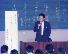
Fig. 2. Lecturing to students at University of Tsukuba in 1995. © University of Tsukuba.
Download figure:
Standard image High-resolution image2. Judicious mind and creative mind
The power of the human mind can be divided into two major categories: "the judicious mind" and "the creative mind".
The judicious mind allows us to analyze and understand how to select and make fair judgments, through the learning of up-to-date information and knowledge; this is non-individualistic and is covered in essence by the body of existing knowledge.
On the other hand, the creative mind allows us to pinpoint core issues and create new ideas through active imagination and acute perceptiveness; this is individualistic and represents a response to the challenge of an unknown and uncertain future.
"The creative mind" is a sine qua non for researchers, whereas it is "the judicious mind" that is indispensable for educators.
There are two types of education: "being taught" and "self-teaching".
"Being taught" is more passive and involves imitation, listening, reading, and remembering. This is how "the judicious mind" is acquired. "Self-teaching", however, is autonomous and, through questioning, considering, searching, and doing, cultivates "the creative mind".
It is "the creative mind" that provides the driving force for progress in science and technology. This has stimulated and sustained the advance of human civilization, although academic education is primarily aimed at nurturing "the judicious mind" in many countries.
I would like to state here my dogmatic assumption regarding the dependence on age of the two different minds, regardless of the differences between individuals (see Fig. 3).

Fig. 3. Judicious mind and creative mind as a functions of age. © Chuokoron-Shinsha, Inc.
Download figure:
Standard image High-resolution imageFor example, let us say we work from the age of 20 to 70 and, on a scale of 0 to 100%, "the creative mind" is at 100% at the age of 20 and decreases with age to reach 0% at the age of 70. Meanwhile, "the judicious mind" is at 0% at the age of 20 and increases with age to reach 100% at the age of 70. Since "the creative mind" must play an important role in research, most Nobel laureates in sciences have done their prizewinning work below 45 years of age. I discovered the Esaki tunnel diode at the age of 32 and invented man-made superlattices at the age of 44. Albert Einstein undertook three significant studies, the special theory of relativity, the photon theory of light, and the theory of Brownian motion, at the age of 26.
Given these conditions, "the declining creative mind" and "the rising judicious mind" will become equal when they intersect at the age of about 45. If the two minds are in harmony with each other, this point in time will be "the zenith of life". However, if the two minds are in conflict with each other at this time, a mid-life crisis will be brought about.
3. Science and technology
Generally speaking, natural science is an institutionalized means of inquiry that creates knowledge providing a systematic understanding of the physical environment, whereas technology or engineering is the application of that scientific knowledge to the resolution of social and economic problems.
Science and technology have thus made invaluable and complementary contributions to our improved living standards in terms of economic development, provision of health care and other social amenities, improving our living conditions generally, and mitigating some of the worst effects of natural and man-made disasters.
It is obvious that the interface between science and technology plays the most important role in the mutual transfer of valuable information and knowledge. However, there are many cases where the interface is hardly established because scientists focusing on basic research and engineers focusing on a practical approach do not communicate well with each other. In consideration of this unfortunate fact, interdisciplinary research around the interface has been given particular emphasis in my studies.
Our modern civilization has indeed created an elaborate artificial environment by providing a large number of tools, instruments, and machines, as well as information–processing systems, which have replaced most of our physical and mental labor. Looking back over the course of the development of technology, history clearly shows that our ancestors made efforts toward pushing human faculties to the limit.
Our growing understanding of the genetic code DNA and its implications has created the potential for us to live a longer and healthier life. Clearly, we are pushing our longevity to the limit in the field of biomedical technology in the 21st century.
Albert Einstein stated, "Development of Western science is based on two great achievements: the invention of the formal logical system (in Euclidean geometry) by the Greek philosophers and the discovery of the possibility to find out causal relationships by systematic experiment (during the Renaissance)".
Natural science can be classified into two major categories: physical science and life science. Einstein's statement can be applied primarily to physical science since we know that the universe is principle-controlled, where everything is connected by cause and effect, obeying rational rules. On the other hand, life science is somehow phenomenological, involving classification or grouping because of the intricacy of living things.
The origin of physical science is probably the natural philosophy of the ancient Greeks. On the other hand, the origin of life science can be traced to the development of medicines. From ancient times, human beings have been destined to battle with emerging diseases by making good use of available medicines. However, starting with the development of molecular biology in the 1940s, which analyzes living organisms at the molecular level, biological study including biomedical research has been making remarkable progress and thus the difference in nature between physical science and life science has been reducing considerably.
4. Personal history and publications
(1) 1925–1947 "Childhood and Adolescence": I was born in Osaka and lived in Kyoto until finishing high school. I then moved to Tokyo and graduated from the University of Tokyo in 1947.
(2) 1947–1960 "Youth": After graduating, I started to work at Kobe Kogyo Corporation, where I studied semiconductors1) until I joined Sony in 1956. There, I discovered the Esaki tunnel diode2,3) in 1957, which was to be my Ph.D. thesis at the University of Tokyo, and for which I was later awarded the 1973 Nobel Prize in Physics.
(3) 1960–1992 "Life in New York": I moved to the United States in 1960, joining IBM T. J. Watson Research Center, New York, where I pioneered "designed semiconductor quantum structures such as resonant tunnel diodes and man-made superlattices",7–30) opening up a new frontier in the field of semiconductors for which I was awarded the 1998 Japan Prize.
(4) 1992–Present "New Life in Tsukuba, Tokyo, and Yokohama": When I was voted to be President University of Tsukuba, I returned to Japan in 1992. I completed my presidency at University of Tsukuba in 1998 and subsequently assumed the post of President Shibaura Institute of Technology from 2000 to 2005 and have been President Yokohama College of Pharmacy since 2006. Meanwhile, I have been holding the Chairmanship of the Science and Technology Promotion Foundation of Ibaraki since 1998 and also serving as President the Science Academy of Tsukuba since its inception in 2000.
In 2000, I was appointed to the Chairman of the National Commission on Educational Reform by the Prime Minister. "Develop the talent of individuals and foster creative individuals" was one of our 17 proposals for changing education.
5. Student days
I was just twenty years old when the Second World War ended, so I belong to the generation that grew up in Japan during the war, graduating immediately after the defeat and going out to a world in turmoil. Our particular generation must surely have undergone unique experiences of both war and peace. Therefore, we have experienced shortages and affluence, as well as restrictions and freedom.
Under wartime conditions, when death and destruction were all too close to us, we seriously questioned ourselves: What should be our top priority, the most essential thing of all, in this life? We somehow thirsted for knowledge of the truth of the universe, believing in the immense potentiality of the creative mind. I myself was fascinated by the progress of science, for science has enhanced our human abilities very substantially by using the power of the brain. I dreamed of becoming a student with an inquiring scientific mind, so I entered the Physics Department of Tokyo Imperial University in September 1944. There was no entrance examination due to the war.
On the evening of March 9, 1945, and early the next morning, the city of Tokyo suffered a horrendous incendiary bomb attack by the US Air Force, resulting in nearly one million victims, including a hundred thousand dead. I was bombed out of my lodgings but, fortunately, I was able to rescue most of my personal belongings. Although many people had experienced a sleepless night, at the university Prof. Tsutomu Tanaka, surprisingly, began to teach his course of classes on Experimental Physics at 8:00 a.m. sharp as though nothing had happened. We were forcibly immersed in the world of physics, leaving the human calamity outside.
We were taught that learning had to be a top priority, no matter what happened. It was then that we realized how awesome was the academicism of Tokyo Imperial University.
As a matter of fact, I turned twenty just two days later, on March 12, 1945. In the 1940s when I was a student at the university, the revolutionary knowledge of "Quantum Mechanics" developed by Heisenberg and Schrödinger had not yet been widely disseminated, at least not in Japan. Nevertheless, we students were really fascinated by the introduction of novel concepts such as the "Energy Quantum" by Planck, the "Quantum Model of Atoms" by Bohr, the "Uncertainty Principle" by Heisenberg, the "Duality of Matter" (the wave nature of electrons) by de Broglie, the "Exclusion Principle" by Pauli, and so forth. We recognized the far-reaching influence of the "Quantum Revolution" that had occurred earlier in the 20th century.
Now, the main purpose of receiving a proper education is to obtain adequate answers to the following questions as they are indispensable to planning the course of life:
What should I do with my life?
What am I best at?
What is my mission in life?
The course of life can be considered to be a drama in which you play the leading role. The point at issue is who writes the scenario, you or somebody else? In a democratic society you can decide your own future. You yourself should be the scenario — writer. You must carefully prepare a scenario under which you will have the possibility of displaying your ability to the maximum in your lifetime. You ought to make the best use of all available options. In 1947, when I graduated from university, Japanese industry was in a state of disaster as the war had ended in our defeat. Nevertheless, I wrote a unique scenario for myself, that I would put the new knowledge of quantum mechanics to practical use. I thought this approach would be not only the best use of my ability but also provide some help to our troubled industry. It is true, though, that life's journey does not always proceed according to plan because of chance occurrences. You should make sure you seize every chance which is thrown in your way, as chance will play an important role in your life.
In 1947, after graduation, I started my own life as a researcher in the electronics industry, where I explored the possibility of creating quantum electron devices. Coincidentally, 1947 was the year in which the epoch-making transistor was invented at Bell Telephone Laboratories.34)
The advent of the transistor was a great breakthrough. There is a tendency, especially in stable societies, to assume that the future is simply a natural extension of the past and the present. However, the transistor is substantially different from the vacuum tube, which was widely used at that time, and no amount of research and improvement of the vacuum tube could have led to the birth of the transistor. This taught us an important lesson: in periods of great change, innovations and breakthroughs shape and form the future. Needless to say, it is the power of individual creativity which plays the decisive role in this process.
6. Discovery of Esaki diode
It was the advent of the transistor that inspired me to study semiconductors at an early stage.1) Around 1950, the technology of Ge p–n junctions had been developed; so efforts were being made to understand the junction properties, including the breakdown in the reverse direction. McAfee, Ryder, Shockley, and Sparks35) at Bell Telephone Laboratories all asserted that the low-voltage breakdown in Ge junctions resulted from the Zener mechanism,36) that is to say, interband electron tunneling from the valence band in the p-region to the empty conduction band in the n-region.
However, later studies did not support the Zener mechanism and it was therefore concluded that the breakdown in Ge junctions was always due to an avalanche mechanism.37) Although Zener had proposed quantum mechanical interband electron tunneling as an explanation for dielectric breakdown in 1934, this sophisticated electron tunneling mechanism had never been proved to be important in reality. We may call this proposal "a creative failure".
Although that was still the situation in 1956, somehow I had become convinced that electron tunneling must be observable under suitable conditions, so I risked investigating the tunneling mechanism in narrow Ge p–n junctions. Since the junction width is approximately inversely proportional to  , where N is the impurity concentration, we explored heavily-doped p–n junctions, pushing doping to the limit.
Figure 4 shows the current–voltage characteristics for diodes of three kinds. I first obtained a backward diode which was more conductive in the reverse direction than in the forward direction, as shown in Fig. 4(b). The junction width of that diode was 20 nanometers or less; the possibility of an avalanche was completely excluded because the breakdown occurred well below the threshold voltage for electron–hole pair production.37) When I increased the doping level further, the junction width narrowed down to about 10 nanometers. At that junction width, the current-flow mechanism was convincingly tunneling not only in the reverse direction but also in the low-voltage range in the forward direction, giving rise to a prominent current–peak, as shown in Fig. 4(c). The change in the energy diagram with the increase in applied voltage is shown in Fig. 5. Since a current–peak associated with a negative resistance had never been predicted, the Esaki diode — the very first quantum electron device — came as a total surprise in 1957.2)
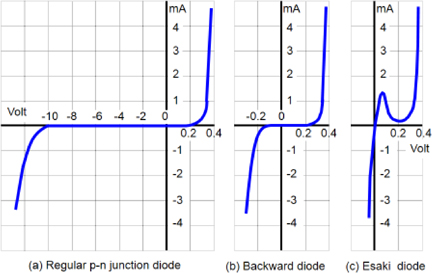
Fig. 4. Current–voltage characteristics for diodes of three kinds.
Download figure:
Standard image High-resolution image
Fig. 5. Energy diagram of the Esaki tunnel diode: (a) No applied voltage. (b) Applied voltage Vp at the current peak. (c) Applied voltage Vv at the current bottom. (d) A higher forward applied voltage. © IEEE.
Download figure:
Standard image High-resolution imageAt this point, I would like to mention an interesting episode which took place while I was busy measuring the diode characteristics. Hanging on the wall near my desk, unintentionally, was a woodblock print known as "The Breaking Wave Off Kanagawa" by Hokusai (1760–1849), one of the greatest masters of Ukiyo-e. The woodblock print was one of a set entitled "Thirty-Six Views of Fuji", considered to be the culmination of Hokusai's art. I suddenly discovered that, when the coordinate axes were superimposed as shown in Fig. 6, the outline of the wave bore a striking resemblance to the current–voltage curve of the Esaki diode as shown in Fig. 7.

Fig. 6. "Breaking Wave Off Kanagawa" woodblock — printed around 1831 by Katsushika Hokusai (1760–1849). The shape of this dramatic wave resembles the current–voltage characteristic of the Esaki diode. © IEEE.
Download figure:
Standard image High-resolution image
Fig. 7. Current–voltage characteristic of an Esaki diode.
Download figure:
Standard image High-resolution imageFigure 8 shows a photograph of myself, my assistant, and a foreign visitor watching the current–voltage characteristic around the time the Esaki diode was discovered (August 1957).
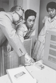
Fig. 8. Watching the current–voltage characteristic with my assistant Yuriko Kurose (right) and s foreign visitor around the time the Esaki diode was discovered (August 1957). © Chuokoron-Shinsha, Inc.
Download figure:
Standard image High-resolution imageFigure 9 shows a photograph of Walter Brattain's visit to Tokyo Tsushin Kogyo (now Sony) in 1957.

Fig. 9. Walter Brattain's visit to Tokyo Tsushin Kogyo (now Sony) in 1957. © Sony Corporation.
Download figure:
Standard image High-resolution imageIt is said that Democritus, the great Greek philosopher of the 5th century B.C., stated, "Everything existing in the Universe is the fruit of chance and of necessity" according to the 1965 Nobel Prize-winning French biologist Jacques Monod (in his book "Chance and Necessity", published in 1971).
It is true that in my scientific research, the achievement of the Backward diode was indeed the fruit of necessity, whereas the discovery of the Esaki diode could be that of chance. In basic research, it should be emphasized that the most valuable result is, in fact, the unexpected fruit of chance — and this will always play an important role in the progress of science.
Louis Pasteur, the great bacteriologist of the 19th century, said "Chance favors the prepared mind". Somehow, I must have paved the way to a mind already prepared to be blessed with such a great chance as the discovery of the Esaki tunnel diode.
We have undertaken shelf-life tests on Esaki tunnel diodes after storage for half a century33) and have observed minute but tangible reductions in the tunnel current. The reduction was attributed to 0.25% widening of the tunnel path. The observed widening, equivalent to about one-tenth of the lattice constant, apparently does not affect the function of the diode at all. We are pleased to report that a Sony FM radio (EFM-117) made in the early 1960s, as shown in Fig. 10, still works beautifully: it was equipped with one Esaki diode serving as a local oscillator and eleven germanium transistors. This is a gratifying confirmation of the longevity of the Esaki tunnel diode.
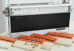
Fig. 10. Sony radio (EFM-117) made with one Esaki diode and eleven transistors in the early 1960s, in front of which are discrete Esaki diodes made in 1960. © Chuokoron-Shinsha, Inc.
Download figure:
Standard image High-resolution imageIn 1958, I visited Europe to participate in the International Conference on Solid State Physics and Its Applications in Electronics and Telecommunications, held in Brussels on June 2–7.
William Shockley, Nobel Laureate, gave the keynote lecture in the opening session of the conference. It was then that the Esaki tunnel diode suddenly leaped into fame because of Shockley's glowing reference:
"The most beautiful demonstration of the Zener effect so far achieved is to be presented at this symposium by L. Esaki of Tokyo. Esaki has studied p–n junctions which are very heavily doped on both sides, so that there is a built-in field of the order of 5 × 10⁵ V/cm. Under these conditions, current flows by the Zener mechanism even at zero voltage. Esaki finds that as forward bias is increased across the junction, this possibility of direct tunneling disappears and, as a consequence, he observes a predictable negative resistance region".
As a result of his comments, a large audience was attracted to my presentation, and I found myself standing in the spotlight of the semiconductor research community. A photograph of W. Shockley with his wife and myself at the conference is shown in Fig. 11.
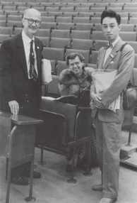
Fig. 11. W. Shockley (48 years old) with his wife and Leo Esaki (33 years old) at the International Conference on Solid State Physics and Its Applications in Electronics and Telecommunications in 1958. © Chuokoron-Shinsha, Inc.
Download figure:
Standard image High-resolution imageAfter Europe, I traveled to the United States and visited the Bell Telephone Laboratories where the transistor was born. The following are the words which appear below the bust of Alexander Graham Bell, the Scottish-born American audiologist best known as the inventor of the telephone, which stands in the foyer of the main entrance to Bell Laboratories: "Leave the beaten track occasionally and dive into the woods. You will be certain to find something that you have never seen before".
In 1959, a fever of research into the Esaki tunnel diode spread across the United States, and a number of research positions in industry as well as academia were offered to me. I was tempted to leave the Japanese beaten track and dive into the American woods. Figure 12 shows the bust of Alexander Graham Bell and Fig. 13 shows myself, L. V. Keldysh, and J. Bardeen at a study meeting on tunneling in Philadelphia.
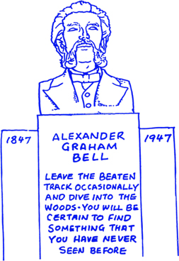
Fig. 12. Bust of Alexander Graham Bell in the foyer of the main entrance to Bell Laboratories.
Download figure:
Standard image High-resolution image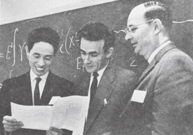
Fig. 13. Myself, the Russian theorist, L. V. Keldysh, and John Bardeen (from left to right) at a study meeting on tunneling in Philadelphia in 1959. © The Japanese Association for American Studies.
Download figure:
Standard image High-resolution image7. Moving to the United States and superlattice research
In 1960, I risked moving to the United States, accepting an offer from IBM T. J. Watson Research Center, New York, which would provide a desirable research environment to realize the scenario of putting quantum principles into practice to which I had committed myself. Along this line, an ambitious long-term research project based on my novel invention was emerging as I gained complete freedom to select the research subject because of my appointment to the IBM Fellowship in 1967.
In 1969, myself and Tsu proposed a semiconductor superlattice,7–30) a "man-made periodic quantum structure" which was engineered by the growth technique of molecular beam epitaxy (MBE) after designing the structure in accordance with the principles of quantum theory in such a way as to exhibit unprecedented electronic properties. The proposal was based on Bloch's golden rule that the periodic potential in a crystal lattice determines its electronic properties. The lattice constant of this proposed superlattice, which we could decide according to our intention was in the range of 1–10 nm, substantially longer than that of the host crystal but shorter than the electron phase-coherent length. This long lattice constant of our superlattice plays a crucial role in giving rise to electric quantization or the macroscopic quantum effect.
Originally, two types of synthesized superlattices: doped and compositional, were envisioned as shown in Fig. 14. However, all our experimental studies were limited to compositional superlattices.
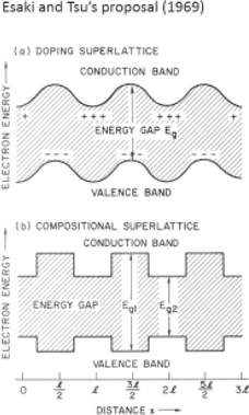
Fig. 14. Two types of synthesized superlattices proposed by Esaki and Tsu in 1969. © Royal Swedish Academy of Sciences.
Download figure:
Standard image High-resolution imageThe introduction of the superlattice potential clearly perturbs the band structure of the host materials. Since the superlattice period, l, is usually much greater than the original lattice constant, the Brilliouin zone is divided into a series of minizones, giving rise to narrow allowed subbands, E1 and E2, separated by forbidden regions in the conduction band of the host crystal, as shown at the top of Fig. 15. Thus, this results in a highly perturbed energy-wave vector relationship for conduction electrons, as schematically illustrated at the bottom of Fig. 15. The dynamics of conduction electrons in such narrow bands was analyzed with a simplified path integration method.
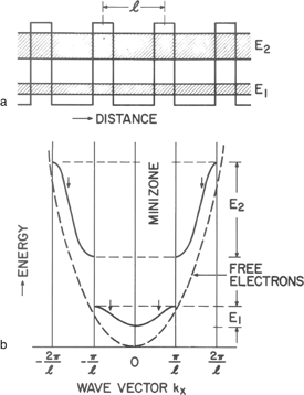
Fig. 15. Potential profile of a superlattice (top) and its energy-wave vector relationship in the minizones. © Royal Swedish Academy of Sciences.
Download figure:
Standard image High-resolution imageNow, I would like to point out one of the most important aspects of the superlattice. Because of the large lattice constants of superlattices, the condition of electric quantization (the formation of the Wannier–Stark ladder or the occurrence of Bloch oscillation), eEl > ħ/τ, could be fulfilled with reasonable field strengths, E ≦ 104 V/cm, although this condition is hardly attainable in ordinary crystals, where, ħ denotes Planck's constant, τ is the scattering time, and l is the lattice constant.
Then, myself and coworkers obtained the relationship between the applied field (voltage) and the average electron drift velocity (current) as shown in Fig. 16, indicating the occurrence of a differential negative resistance.

Fig. 16. Theoretical current–field (voltage) characteristic. © Royal Swedish Academy of Sciences.
Download figure:
Standard image High-resolution imageLater, this current–voltage characteristic was experimentally confirmed using a superlattice with a lattice constant of l = 7 nanometers, as shown in Fig. 17.

Fig. 17. Observed current–voltage characteristic for a superlattice with a lattice constant of 7 nm. © Nobel Foundation.
Download figure:
Standard image High-resolution imageSince the one-dimensional periodic potential is introduced along the superlattice axis (perpendicular to the deposited plane layers), elegantly simple examples in one-dimensional quantum physics, for instance, resonant electron tunneling, the Kronig–Penney band model, Stark localization, or Bloch oscillation, which had all remained textbook exercises, could, for the first time, be practiced in a laboratory: Do-it-yourself quantum mechanics had become possible.
This approach makes "gedanken experiments" a reality, so the proposed superlattice has apparently fulfilled a great dream in semiconductor research by opening up vast frontiers with new opportunities for exploration.
Bloch oscillation in semiconductor superlattices38) is worthy of notice because of the macroscopic quantum effect similar to the Josephson effect observed in weakly coupled superconductors. In both cases, if a DC electric field is applied to the system, an AC field is generated.
In Bloch oscillation, the frequency, v is given by eFl/ħ = Fl/2Φ0, where F is the applied electric field, l is the superlattice constant, ħ denotes Planck's constant, and Φ0 is the unit of the flux quantum, whereas in the Josephson effect, the frequency, v is given by 2eV/ħ = V/Φ0, where V is the applied voltage.
Our pioneering research on superlattices and quantum wells in the 1970s and 1980s triggered a wide spectrum of experimental and theoretical investigations, creating a new frontier in semiconductor research. This resulted in not only the observation of a number of intriguing new phenomena such as differential negative resistance, high electron mobility, large excitonic binding energies, large Stark shifts, distinct Wannier–Stark ladders, and Bloch oscillations,38) but also the emergence of a new class of transport and optoelectronic devices such as high electron-mobility transistors (HEMTs), high-speed resonant tunnel diodes, high-performance injection lasers with quantum wells, quantum-cascade lasers,39) and high-power quantum-cascade superlattice lasers.40)
Rita Claudia Iotti and Fausto Rossi made the following remark in the beginning of their paper41) on quantum-cascade lasers. "Since the seminal paper of Esaki and Tsu,7) semiconductor-based nanometric heterostructures have been the subject of impressive theoretical and experimental activity, due to their high potential impact in both fundamental and applied research".
The US Army Research Office also praised the superlattice concept. Excerpts from the document "Superlattice Story" prepared by them in 1997 are as follows:
"The superlattice concept proposed (in February 1969) under Army sponsored research triggered a revolution in solid state physics....
The impact of Esaki's research has been profound. The superlattice concept precipitated more than 10,000 publications and is directly involved in some 465 patents in the U.S. alone, by the end of 1996.... The superlattice may be regarded as the trunk of a genealogical tree of quantum effect devices,.... The characteristic dimensions of superlattice devices certainly served as the precursor of today's "smaller and smaller" nanotechnology emphasis". (In 1997, this document was distributed for the promotion of the US National Nanotechnology Initiative.)
In 1998, I was awarded the Japan Prize for the creation and realization of the concept of man-made superlattice crystals which led to a generation of new materials with useful applications. A photograph of the banquet with Their Majesties the Emperor and Empress of Japan held in celebration of the 1998 Japan Prize is shown in Fig. 18.
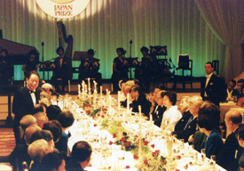
Fig. 18. Banquet with Their Majesties the Emperor and Empress of Japan held in celebration of the 1998 Japan Prize. © The Japan Prize Foundation.
Download figure:
Standard image High-resolution imageAn interdisciplinary journal, "Superlattices and Microstructures", has been published continuously since 1986 by Academic Press, indicating the flourishing nature of the field.
8. Evaluation of research
My research activities started in 1947 when I graduated from the University of Tokyo and virtually ended in 1992 when I returned to Japan to assume the post of President of University of Tsukuba. It may be informative to evaluate my research activities over half a century using citation data from Thomson Reuters' "Web of Science Core Collection".
According to the data, 225 of my papers were published and cited in 7,905 publications as of December 31, 1992, and in 16,566 publications as of August 31, 2014. Therefore, the average "times cited" per paper significantly increased from 35.1 in 1992 to 73.6 in 2014.
My own publication–distribution by year shown in Fig. 19 indicates the virtual halt in new publications when I returned to Japan in 1992. However, the citation–distribution by year shown in Fig. 20 indicates that the publications are still being frequently cited even though I am no longer writing published papers.
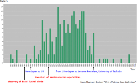
Fig. 19. Esaki's publications — distribution by year.
Download figure:
Standard image High-resolution image
Fig. 20. Esaki's citations — distribution by year.
Download figure:
Standard image High-resolution imageMy research after 1970 was focused on designed quantum structures such as superlattices; thus, as of August 31, 2014, 84% of the citations and 77% of my publications are related to studies in this field.
We should now consider the cumulative number of the "times cited" for each paper. Generally, this indicates the long-term impact of research.
The numbers of papers cited to 300–500, 500–1000, 1000–2000, and more than 2000 times are 2, 5, 2, and 1, respectively. Apparently, these top ten papers were cited in 9,303 publications, more than half of the total of 16,566 publications in the relevant fields. The details of the top ten papers including "times cited" are listed in Table I and also shown in Fig. 21.
Table I. Times cited for Esaki's 10 major papers.
| No. | Authors and titles of papers | Times cited 12–31–'92 | Times cited 08–31–'14 |
|---|---|---|---|
| 1 | L. Esaki, "New Phenomenon in Narrow Germanium p–n Junctions" Phys. Rev. 109, 603 (1958) (Ref. 2) | 319 | 729 |
| 2 | L. Esaki and R. Tsu, "Superlattice and Negative Differential Conductivity in Semiconductors" IBM J. Res. Dev. 14, 61 (1970) (Ref. 7) | 844 | 2,365 |
| 3 | R. Tsu and L. Esaki, "Tunneling in a Finite Superlattice" Appl. Phys. Lett. 22, 562 (1973) (Ref. 9) | 520 | 1,576 |
| 4 | L. L. Chang, L. Esaki and R. Tsu, "Resonant Tunnelling in Semiconductor Double Barriers" Appl. Phys. Lett. 24, 593 (1974) (Ref. 11) | 545 | 1,311 |
| 5 | L. Esaki and L. L. Chang, "New Transport Phenomenon in a Semiconductor Superlattice" Phys. Rev. Lett. 33, 495 (1974) (Ref. 12) | 213 | 534 |
| 6 | G. A. Sai-Halasz, R. Tsu and L. Esaki, "A New Semiconductor Superlattice" Appl. Phys. Lett. 30, 651 (1977) (Ref. 16) | 129 | 332 |
| 7 | G. Bastard, E. E. Mendez, L. L. Chang, L. Esaki, "Exciton Binding Energy in Quantum Wells" Phys. Rev. B 26, 1974 (1982) (Ref. 22) | 308 | 684 |
| 8 | G. Bastard, E. E. Mendez, L. L. Chang, L. Esaki, "Variational Calculations on a Quantum Well in an Electric-Field" Phys. Rev. B 28, 3241 (1983) (Ref. 24) | 249 | 657 |
| 9 | L. Esaki, "A Bird's-Eye View on the Evolution of Semiconductor Superlattices and Quantum Wells" IEEE J. Quantum Electron. 22, 1611 (1986) (Ref. 30) | 161 | 355 |
| 10 | H. Munekata, H. Ohno, S. von Molnar, A. Segmuller, L. L. Chang, L. Esaki, "Diluted Magnetic III–V Semiconductors" Phys. Rev. Lett. 63, 1849 (1989) (Ref. 31) | 11 | 760 |
| Number of citations of top 10 papers | 3,299 | 9,303 | |
| Total number of citations of all papers | 7,905 | 16,566 |
1 The discovery of the Esaki tunnel diode.
2 The invention of a man-made superlattice.
3–5 Early papers related to the superlattice and resonant tunneling.
6 Type II superlattices such as the In1−xGaxAs–GaSb1−yAsy system.
7–8 Theoretical analyses on quantum wells.
9 A review.
10 A challenging attempt to introduce magnetism into III–V semiconductor physics.
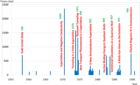
Fig. 21. Esaki's ten major papers: year of publication vs times cited as of August 31, 2014.
Download figure:
Standard image High-resolution imageThe cumulative number of "times cited" as a function of year for Papers 1–5 in Table I is shown in Fig. 22. A similar curve for Papers 6–10 is shown in Fig. 23. It is interesting to see that Papers 2–5 needed a long take-off run of more than ten years.
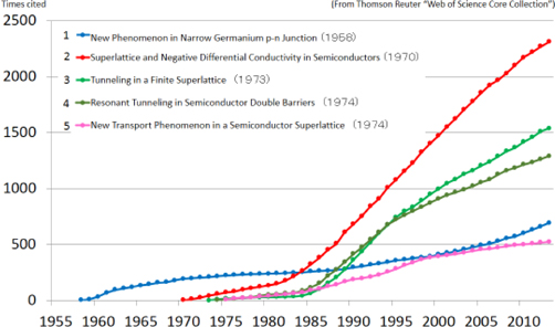
Fig. 22. Cumulative number of "times cited" as a function of year for Papers 1–5.
Download figure:
Standard image High-resolution image
Fig. 23. Cumulative number of "times cited" as a function of year for Papers 6–10.
Download figure:
Standard image High-resolution imageVarious types of band-edge discontinuity are shown in Fig. 24. Paper 6 discusses type II superlattices (b and c in the figure), such as the In1−xGaxAs–GaSb1−yAsy system, where the interaction of the conduction band in one host material with the valence band in the other host material plays an important role. Paper 10 reported novel magnetic III–V semiconductors for the first time in the world, paving the way to the introduction of magnetism into III–V semiconductor physics, spintronics. The considerable recent increases in the "times cited" for Papers 6 and 10 indicate that these fields are now flourishing.
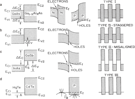
Fig. 24. Discontinuities of band-edge energies at four types of hetero interfaces (a)–(d): band offset (left), band bending due to carrier confinement (center), and superlattices (right). © Royal Swedish Academy of Sciences.
Download figure:
Standard image High-resolution imagePaper 2, our most "times cited" paper, Esaki and Tsu's "Superlattice and Negative Differential Conductivity in Semiconductors", was rejected for publication in Physical Review in 1969 on the basis of the following referee's comment:
"In summary, then, the paper is highly speculative and presents little material not already known and understood. While one should not arbitrarily dismiss speculative papers per se, in a case such as the present where an experimental test of the speculation is close at hand, I believe one should incorporate the material of the paper into one which reports the performance of the device so constructed. The paper as it now stands has the flavor of a publication whose principal purpose is to establish priority of an interesting idea. Such arguments can be settled by reference to internal laboratory reports, and already overcrowded journals should not be burdened with these matters".
Recently, however, American Physical Society highly praised the achievement of designed semiconductor superlattice structures as described in the APS Historic Sites Plaque shown in Fig. 25.
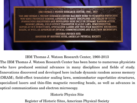
Fig. 25. American Physical Society Historic Sites Plaque in the lobby of IBM T. J. Watson Research Center in New York. © IBM.
Download figure:
Standard image High-resolution imageA similar plaque from IEEE also lauds "superlattice crystals" as shown in Fig. 26.
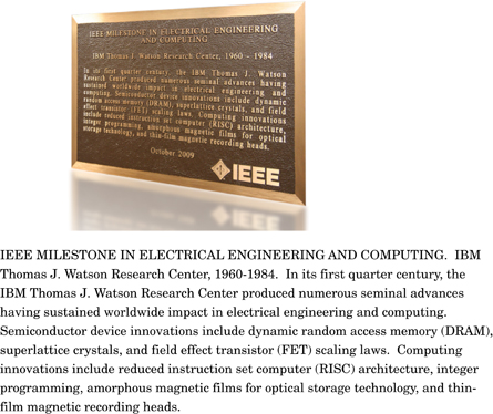
Fig. 26. IEEE Milestone Plaque in the lobby of IBM T. J. Watson Research Center in New York. © IBM.
Download figure:
Standard image High-resolution image9. Nanoscience and the Leo Esaki Prize
The continuing progress in nanolithography has enabled the creation of nanometer-scale features on microprocessor chips, and the development of the scanning tunneling microscope in the 1980s dramatically improved access to the nano-world. Those developments inspired the advent of nano scale science and engineering in the 1990's.
Nanoscience and nanotechnology encompass the observation, understanding, design, fabrication, and utilization of nanometer-scale objects. There are many exciting challenges in research in the nano-world with a strong interdisciplinary flavor.
The prefix "nano" means one billionth. One nanometer is 1/1,000,000,000 of a meter. Since the limit of visibility of the human eye is 10 µm, we can see a human hair that is 50 µm across.
As shown in Fig. 27, one should remember the following:
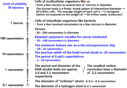
Fig. 27. Comparative sizes — from cells to atoms.
Download figure:
Standard image High-resolution image- 1)The cell size of multicellular organisms like us is around 10 µm.
- 2)The cell size of unicellular organisms like bacteria is around 1 µm.
- 3)The size of viruses is around 100 nm. A virus is indeed a nano size creature.
Nanoscience as a leading interdisciplinary research field in the 21st century is expected to make seminal contributions to society through the development of new innovative technologies.
The Leo Esaki Prize was therefore established in 2003 with the support of Sekisho Corporation to contribute to advancement of the nano-field by honoring epoch-making achievements in Japan in nanoscience or nanotechnology.
The winners of the Leo Esaki prize (the title at that time) have been as follows:
• The 2004 Prize (1st) to Dr. Hiroyuki Sakaki, Professor, Institute of Industrial Science, the University of Tokyo, and Dr. Yasuhiko Arakawa, Professor, Research Center for Advanced Science and Technology, The University of Tokyo, for their work on Pioneering studies on semiconductor nanoelectronics devices including seminal research contributions to advanced devices based on quantum wire and quantum dot structures.
• The 2005 Prize (2nd) to Dr. Teruo Okano, Professor, Institute of Advanced Biomedical Engineering and Science, Tokyo Women's Medical University, for his work on Cell sheet engineering produced by molecular design of the nano-biointerface.
• The 2006 Prize (3rd) to Dr. Tsuneya Ando, Professor, Department of Physics, Tokyo Institute of Technology, for his work on Theoretical study of electronic properties of quantum nanostructures.
• The 2007 Prize (4th) to Dr. Seigo Tarucha, Professor, Department of Applied Physics, The University of Tokyo, for his work on Development of artificial atoms and molecules and challenging work for quantum computing.
• The 2008 Prize (5th) to Dr. Kunio Takayanagi, Professor, Department of Physics, Tokyo Institute of Technology, for his work on Pioneering study on surface as nano-materials' phases.
• The 2009 Prize (6th) to Dr. Susumu Noda, Professor, Department of Electronic Science and Engineering, Kyoto University, and also Director, Photonics and Electronics Science and Engineering Center, Kyoto University, for his work on World-foremost study on photonic crystals controlled in nanometer–scale.
• The 2010 Prize (7th) to Dr. Makoto Fujita, Professor, Department of Applied Chemistry, School of Engineering, The University of Tokyo, for his work on Pioneering the use of self-assembly to engineer the nanoscopic structure of matter.
• The 2011 Prize (8th) to Dr. Satoshi Kawata, Professor, Department of Applied Physics, Osaka University, and also Chief Scientist, Advanced Science Institute, RIKEN, for his work on Near-field nano-optics and plasmonics.
• The 2012 Prize (9th) to Dr. Kazunori Kataoka, Professor, Department of Materials Engineering, Graduate School of Engineering/Center for Disease Biology and Integrative Medicine, Graduate School of Medicine, The University of Tokyo, for his work on Supermolecular nanostructures as drug and gene carriers for targeting therapy of intractable diseases.
• The 2013 Prize (10th) to Dr. Susumu Kitagawa, Director, Institute for Integrated Cell-Material Sciences, and also Professor, Department of Synthetic Chemistry and Biological Chemistry, Graduate School of Engineering, Kyoto University, for his work on Pioneering and developing studies on novel porous materials.
• The 2014 Prize (11th) to Dr. Jaw-Shen Tsai, Team Leader, Center for Emergent Matter Science, RIKEN and Dr. Yasunobu Nakamura, Professor, Research Center for Advanced Science and Technology, The University of Tokyo, for their work on Pioneering of the superconducting bit system.
10. How to win a Nobel Prize
Here is a list of "five don'ts" which anyone with an interest in realizing his or her creative potential should follow. Who knows, it may even help you win a Nobel Prize.
Rule number one: Don't allow yourself to be trapped by your past experiences. Don't hold on too tightly to your preconceived notions. If you allow yourself to get caught up in social conventions or circumstances, you will not notice the opportunity for a dramatic leap forward when it presents itself. You should be a free spirit.
Looking back at history, most laureates have received the Nobel Prize for work done during their thirties. In my case, I was 32 years old when I developed the "Esaki tunnel diode". The point that I am trying to make is that, because of their candor, younger people are able to look at things with a clearer vision that is not clouded by social conventions and past history.
Rule number two: Don't allow yourself to become overly attached to any one authority in your field — a great professor, perhaps. By becoming closely involved with a great professor, you risk losing sight of yourself and may forfeit the free spirit of youth. Although a great professor may be awarded the Nobel Prize, it is unlikely that subordinate researchers will ever receive it.
Rule number three: Don't hold on to what you don't need. The information-oriented society facilitates easy access to an enormous amount of information. The brain can be compared to a personal computer with an energy consumption of about 20 watts. Although the brain occupies only 2% of the body's weight, it consumes 20% of the total energy expended by the body. In terms of memory capacity or computing speed, the human brain has not really changed much since ancient times.
Therefore, we must constantly be inputting and deleting information, and we should save only truly vital and relevant information. As the president of a university, I have opportunities to meet many people and to exchange meishi (name cards) with them. I try to discard the name cards as soon as possible, so that I always leave maximum memory space open. (I'm kidding, of course.)
Rule number four: Don't avoid confrontation. I myself became embroiled in a dispute with the company for which I was working many years ago. At times, it is necessary to put yourself first and to defend your own position. My point is that fighting is sometimes unavoidable for the sake of self-defense.
Rule number five: Don't forget your spirit of childhood curiosity. It is the most vital component of imagination.
Having listed the five rules, let me say that they do not constitute sufficient conditions for success. They are merely suggested guidelines. Good Luck!
Figure 28 shows me receiving the Nobel Prize in Physics at the Award Ceremony on December 10, 1973.
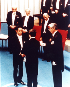
Fig. 28. Nobel Prize Award Ceremony on December 10, 1973. © Chuokoron-Shinsha, Inc.
Download figure:
Standard image High-resolution imageThe 1973 Nobel Prize in Physics was awarded to Leo Esaki (1925–), Ivar Giaever (1929–), and Brian Josephson (1940–) for their research on quantum mechanical electron tunneling. These Nobel Prizes were awarded for the work in their Ph.D. theses. Their average age was 41.7 years in 1973.
The 1973 Nobel Prize in Chemistry was awarded to Ernst Otto Fischer (1918–2007) and Geoffrey Wilkinson (1921–1996) for their pioneering work, performed independently, on the chemistry of the organometallic compounds, so called sandwich compounds. Their average age was 53.5 years.
The 1973 Nobel Prize in Physiology or Medicine was awarded to Karl von Frisch (1886–1982), Konrad Lorenz (1903–1989), and Nikolaas Tinbergen (1907–1988) for their discoveries concerning the organization and elicitation of individual and social behavior patterns. Their average age was 74.3 years.
The average age of Nobel Laureates hints at the date of their achievements. The 1973 Nobel Prize in Physiology or Medicine was awarded for innovative work in the 1940s or before. One of the bestsellers in the field of ethology is "King Solomon's Ring" by K. Lorenz, which was published in 1949.
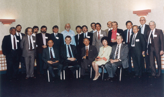
As mentioned earlier, I left IBM Research Center, at Yorktown Heights, New York in 1992 after 32 years' service. A farewell party was held in my honor on May 1st, 1992, as shown in Fig. 29, including my coworkers, L. Chang and R. Tsu, seven Nobel laureates, K. von Klitzing, H. Rohrer, G. Bednorz, I. Giaever, C. N. Yang, W. Lamb, and N. Bloembergen, as well as other friends.
Fig. 29. Farewell party in honor of Leo Esaki at IBM Research Center, New York on May 1st, 1992 (front row from the left) L. Chang, J. Armstrong, L. Esaki, M. Esaki, J. McGroddy; (behind from the left) V. Sadagopan, T. Theis, F. Capasso, G. Bastard, G. Abstreiter, K. von Klitzing, H. Rohrer, H. Sakaki, G. Bednorz, J. Palmer, R. Tsu, L. Eaves, I. Giaever, C. N. Yang, C. Y. Fong, W. Lamb, and N. Bloembergen. © IBM.
Download figure:
Standard image High-resolution image
11. Epilogue
A popular Japanese proverb says, "Learn a lesson from the past" or "The old gives rise to the young". However, the scientific mind says, "Learn a lesson from the future".
We are able to explore the past fully because historical events have been documented. But how can it be possible for us to learn a lesson from the future? The only pathway to the future is to carry out scientific investigation. Through scientific research, we can approach the realm of a future yet to be explored.
Acknowledgements
I sincerely thank all my coworkers over many years for their considerable efforts, especially Professor R. Tsu, the late Dr. L. L. Chang and Professor E. E. Mendez for their contributions to the theoretical treatment, MBE crystal growth, and the quantum-well research, respectively. I also express my gratitude to Dr. Robin E Sowden for polishing the English used in this manuscript and to Ms. Sayaka Miwa and Ms. Yoko Hirose, Thomson Reuters, for the Citation Data in "Web of Science Core Collection".
Appendix
Table A·1 shows the accumulated number of the "times cited" as of August 31, 2014, Thomson Reuters, "Web of Science Core Collection", except Ref. 36 which is based on "cited reference search". Our articles from Ref. 2 to Ref. 32 have been cited more than 100 times.
Table A·1. Accumulated number of the "times cited" as of August 31, 2014. Our articles from Ref. 1 to Ref. 32 are listed in chronological order.
| Reference | Article | Times cited |
|---|---|---|
| 1 | Phys. Rev. 89, 1026 (1953) | 19 |
| 2 | Phys. Rev. 109, 603 (1958) | 729 |
| 3 | Solid-State Electron. 1, 13 (1960) | 106 |
| 4 | Phys. Rev. Lett. 8, 4 (1962) | 130 |
| 5 | Phys. Rev. Lett. 16, 1108 (1966) | 132 |
| 6 | Phys. Rev. 172, 779 (1968) | 100 |
| 7 | IBM J. Res. Dev. 14, 61 (1970) | 2365 |
| 8 | J. Vac. Sci. Technol. 10, 11 (1973) | 155 |
| 9 | Appl. Phys. Lett. 22, 562 (1973) | 1576 |
| 10 | J. Vac. Sci. Technol. 10, 655 (1973) | 125 |
| 11 | Appl. Phys. Lett. 24, 593 (1974) | 1311 |
| 12 | Phys. Rev. Lett. 33, 495 (1974) | 534 |
| 13 | Phys. Rev. Lett. 33, 653 (1974) | 144 |
| 14 | J. Appl. Crystallogr. 10, 1 (1977) | 139 |
| 15 | Phys. Rev. Lett. 38, 1489 (1977) | 122 |
| 16 | Appl. Phys. Lett. 30, 651 (1977) | 332 |
| 17 | Appl. Phys. Lett. 31, 211 (1977) | 167 |
| 18 | Appl. Phys. Lett. 31, 759 (1977) | 196 |
| 19 | Solid State Commun. 27, 935 (1978) | 143 |
| 20 | Phys. Rev. B 18, 2812 (1978) | 226 |
| 21 | Surf. Sci. 98, 70 (1980) | 176 |
| 22 | Phys. Rev. B 26, 1974 (1982) | 684 |
| 23 | Phys. Rev. B 26, 7101 (1982) | 267 |
| 24 | Phys. Rev. B 28, 3241 (1983) | 657 |
| 25 | Appl. Phys. Lett. 47, 415 (1985) | 157 |
| 26 | Phys. Rev. Lett. 55, 2216 (1985) | 101 |
| 27 | Appl. Phys. Lett. 47, 826 (1985) | 226 |
| 28 | Appl. Phys. Lett. 47, 1324 (1985) | 112 |
| 29 | Phys. Rev. B 33, 2893 (1986) | 159 |
| 30 | IEEE J. Quantum Electron. 22, 1611 (1986) | 355 |
| 31 | Phys. Rev. Lett. 63, 1849 (1989) | 760 |
| 32 | Phys. Rev. Lett. 64, 2555 (1990) | 132 |
| 34 | Phys. Rev. 74, 230 (1948) | 332 |
| 35 | Phys. Rev. 83, 650 (1951) | 77 |
| 36 | Proc. R. Soc. London 145, 523 (1934) | 798 |
| 37 | Phys. Rev. 99, 1234 (1955) | 294 |
| 38 | Solid State Commun. 84, 943 (1992) | 223 |
| 39 | Science 264, 553 (1994) | 2741 |
| 40 | Science 276, 773 (1997) | 120 |
| 41 | Phys. Rev. Lett. 87, 146603 (2001) | 157 |
Biographies

Leo Esaki was born in Osaka in 1925. He completed his B.S. in Physics in 1947 and his Ph.D. in 1959, both received from the University of Tokyo. Esaki was an IBM Fellow and engaged in semiconductor research at the IBM Thomas J. Watson Research Center, Yorktown Heights, New York, from 1960 to 1992. Prior to joining IBM, he worked at Sony Corporation, where his research on heavily-doped Ge and Si resulted in the discovery of the Esaki tunnel diode in 1957; this device constituted the first quantum electron device. From 1969 Esaki, with his colleagues, pioneered semiconductor superlattices and resonant tunneling, exploring a new quantum regime in the frontier of semiconductor physics. The Nobel Prize in Physics (1973) was awarded to Esaki in recognition of his pioneering work on electron tunneling in semiconductors and the Japan Prize (1998) was awarded for his invention of semiconductor superlattices. Other awards received include the Nishina Memorial Award (1959), the Asahi Press Award (1960), the Toyo Rayon Foundation Award for the Promotion of Science and Technology (1960), the Morris N. Liebmann Memorial Prize from IRE (1961), the Stuart Ballantine Medal from the Franklin Institute (1961), the Japan Academy Award (1965), the Order of Culture from the Japanese Government (1974), the American Physical Society International Prize for New Materials (1985), the IEEE Medal of Honor (1991), and also the Grand Cordon of the Order of the Rising Sun, First Class, from the Japanese Government (1998). Dr. Esaki was elected a member of the Japan Academy (1975), a Fellow of the American Academy of Arts and Sciences (1974), a Foreign Associate of the National Academy of Science (1976) and the National Academy of Engineering (1977), a member of the Max-Planck-Gesellschaft (1989), and a foreign member of the American Philosophical Society (1991), the Russian Academy of Sciences (1994), the Italian National Academy of Science (1996), and a celebrated member of IEEE Electron Device Society (2012). After returning to Japan, Esaki assumed the positions of President, University of Tsukuba from 1992 to 1998 and President, Shibaura Institute of Technology from 2000 to 2005, and has been President, Yokohama College of Pharmacy since 2006. He has been holding the Chairmanship of the Science and Technology Promotion Foundation of Ibaraki since 1998 and also serving as President, the Science Academy of Tsukuba since its inception in 2000.