Abstract
In this paper, surface-activation-based nanobonding technology and its applications are described. This bonding technology allows for the integration of electronic, photonic, fluidic and mechanical components into small form-factor systems for emerging sensing and imaging applications in health and environmental sciences. Here, we describe four different nanobonding techniques that have been used for the integration of various substrates — silicon, gallium arsenide, glass, and gold. We use these substrates to create electronic (silicon), photonic (silicon and gallium arsenide), microelectromechanical (glass and silicon), and fluidic (silicon and glass) components for biosensing and bioimaging systems being developed. Our nanobonding technologies provide void-free, strong, and nanometer scale bonding at room temperature or at low temperatures (<200 °C), and do not require chemicals, adhesives, or high external pressure. The interfaces of the nanobonded materials in ultra-high vacuum and in air correspond to covalent bonds, and hydrogen or hydroxyl bonds, respectively.
Export citation and abstract BibTeX RIS
1. Introduction
Integration, bonding and interconnection of components on heterogeneous substrates have been recognized as a powerful technology to create miniaturized, low-cost, and high sensitivity biomedical- and environmental-sensing and -imaging systems.1) In this technology, system-on-chip, system-in-package, and system-on-package techniques are being utilized to integrate more functions than that in Moore's Law.2) This approach is known as "More-than-Moore" (MtM) (Fig. 1).3) The MtM approach allows for integrating electrical, optical, photonic, mechanical and fluidic devices for more functional or smart sensing and imaging systems.4) At present, commonly used integration technologies such as thermal compression bonding,5,6) fusion bonding,7) plasma bonding,8,9) and adhesive bonding,10) require high pressure,5) elevated temperatures,7) or chemical solvents.10,11) However, for sensing and imaging applications, some major challenges for the integration of electronic, photonic, fluidic and dielectric materials and devices are related to incompatibilities in the size (thickness and surface roughness),12) structure (crystal, amorphous, polycrystalline, orientation),13) plasticity (deformation),5,7) chemical reactivity (hydrophilicity and hydrophobicity),8–11) and thermal stability14) of the various components.

Fig. 1. MtM for heterogeneous integration using surface activated nanobonding.3)
Download figure:
Standard image High-resolution imageThe surface smoothness of electronic (silicon) and photonic (silicon, germanium and gallium arsenide) materials is better than that of microelectromechanical (glass) and fluidic (glass and polymers) materials. However, the plasticity of the later group of materials is higher than that of the former.15–18) These characteristics result in difficulties in integrating electronic and photonic materials when an external force is required. Also, while the thermal stability of the electronic and photonic materials is considerably higher than that of polymers, the lattice mismatch and structure of electronic and photonic materials is crucial when integrating them. Also, mismatches in the coefficients of thermal expansion are problematic when heating is required in the integration process. Furthermore, chemical reactivity of the surface is a function of surface morphology and bonding atmosphere, which determines bonding spontaneity in the integration. In fact, the commonly used integration technologies mentioned above (such as thermal compression, fusion, or plasma bonding) do not provide the required (1) high bond strength, (2) high electrical conductivity, (3) hermetic sealing, (4) sub-micrometer alignment accuracy, and (5) optical transparency of the bonded interface between device and substrate without degrading the performance of individual components in the biosensing and bioimaging systems.
In this paper, we review some of the more promising nanobonding technologies, especially those that can be used in creating sensing and imaging systems for health and environmental applications. In Sect. 2, we describe some of the popular bonding methods. In Sect. 3, we briefly introduce two examples of biosensing and bioimaging systems. In Sect. 4, we describe some important aspects of sample preparation and characterization. Section 5 contains some selected nanobonding results and discussions of some key features of nanobonded systems of materials. Finally, the summary and future perspectives are presented in Sect. 6.
2. Nanobonding methods
Nanobonding is a direct bonding technology based on surface activation. It has capabilities for the integration of diverse materials with improved quality of interface19) being developed for compact biosensing and bioimaging systems. A nanobonding technology refers to bonding of smooth surfaces of similar or dissimilar materials. This technology offers nanometer-scale bonding at lateral dimensions in an ultrahigh vacuum (UHV), or in air at room temperature.19,20) Nanobonding can be classified into four categories. Table I summarizes the categories of the nanobonding. In the first approach (direct adhesion), the mating surfaces are cleaned with an argon fast atom beam (Ar-FAB), and direct adhesion occurs when they are contacted in UHV.19–32) In the second approach (nano-layers adhesion), the surface cleaning and nano-adhesion layer deposition are simultaneously accomplished using an Ar ion source followed by contact in UHV.33–36) In the third approach (sequential plasma activation), the surfaces are cleaned by a radio-frequency (RF) reactive ion etching (RIE) plasma and microwave (MW) neutral radicals at low vacuum and then bonded in air.37–41) In all three approaches, the cleaned surfaces are called the activated surfaces.
Table I. Categories of surface activated nanobonding.
| Type | Activation | Bonding | Materials | |||||
|---|---|---|---|---|---|---|---|---|
| Source | Gas | Ambient | Temperature | Ambient | Applied | |||
| Voltage (kV) | Load (MPa) | |||||||
| Direct adhesion | FAB | Ar | UHV | RT | UHV | 0 | ∼0.1–0.2 | Si/Si,19,21,22) Si/SiO2,23) Si/GaAs,24) Si/InP,25) GaAs/GaP,26) Cu/Cu,27,28) Au/Cu,30) Au/Al,30) Al/Stainless steel,31) Sn–Ag–Cu solders32) |
| Nano-layers adhesion | LEI | Ar | UHV | RT | UHV | Si/Si,33) Si/SiN,33) Si/LiNbO3,34,35) Si/LiTaO336) | ||
| Sequential plasma activation | RF-RIE + MW-NRs | O2, N2 | LV | RT | CRA | 0 | Si/Si,38,39) Si/glass,40) glass/glass,41) Si/SiO2,83) Ge/SiO283) | |
| Hybrid adhesion (SPA+electrostatic) | RF-RIE + MW-NRs | O2, N2 | LV | 150–200 °C | CRA | 1 | Si/glass,15) Ge/glass,16) GaAs/glass42) | |
SPA: sequential plasma activation. FAB: fast atom beam. LEI: low energy ion. RF-RIE: radio-frequency-reactive ion etching. MW-NRs: microwave neutral radicals. UHV: ultra-high vacuum. LV: low-vacuum. RT: room temperature. CRA: clean room air.
The second and third approaches have been developed for ionic materials to minimize their surface activation induced polarization effect. In the fourth approach (hybrid adhesion), the bonded wafers in the third approach are treated with the anodic bonding method, that is, a voltage is applied on the bonded wafers during heating at low temperature, in air.15,16,42) Compared with other existing direct bonding technologies,43,44) the advantages of the nanobonding technology45) are the following.
- (1)Bonding dissimilar materials over wide areas with high bond strength.
- (2)No requirement of applying external pressure, adhesive, heat, or chemicals.
- (3)Sub-micrometer alignment accuracy.
- (4)Biologically compatible (i.e., non-toxic) interface.
- (5)Preserves delicate components and biological specimens.
- (6)Mechanical, electrical, and optical connections on the same surface.
These properties are highly beneficial in bonding and integrating devices from heterogeneous technologies.
High bonding strength offers enhanced tolerance of handling such as grinding and polishing during the fabrication and integration of structures and devices for sensing and imaging systems.45) Submicrometer alignment accuracy enables the integration of nanostructures and devices in micro- and nano-systems. Optical transparency of the bonded materials controls transmitted optical signals,46) which are critical for the analysis of chemical or biological species in optical sensing systems. Another example of optical transparency is for the solar cells applications. The optically transparent material decreases the light reflection at the interface, allowing photons to efficiently travel through subcells, thus enhancing the performance of the subcells. The improved electrical connection between the materials reduces parasitic losses at the interface, resulting in enhanced current flow. Therefore, nanobonding technology is a highly promising technology for combining dissimilar materials, devices or components.
Nanobonding technology has been demonstrated in the integration of diverse materials with different sizes and thicknesses.19,21–28,30–41) In this article, we discuss some of our recent research results in direct bonding of a variety of substrates including silicon, gallium arsenide, copper, gold and glass. We describe results from nanobonding using the first approach (direct adhesion in UHV) and the fourth approach (the third approach followed by electrostatic treatment in air).
3. Biosensors, bioimagers and nanobonding requirements
In this section, we provide two examples of systems being developed for emerging applications in health and environmental sciences. Very briefly, as shown in Fig. 2,47) in this biosensing system, a real world liquid sample such as blood, saliva from a human or water from a river or lake, is pumped into the filtration and concentration microelectromechanical systems (MEMS) module. The processed sample is then inserted into the cell processing module where the cells are extracted. Next, the cells are broken apart, nuclear DNA extracted and chemically processed to provide the required oligonucleotide related to the pathogen to be detected, and then amplified.48–52) The double-stranded DNA is then denatured to provide single-stranded (SS) oligonucleotides which are then pumped into a microfluidic channel53) to the BioFET sensors. The BioFETs were previously functionalized with the matching SS oligonucleotide for possible hybridization. If the pathogen to be sensed is present in the processed real-world sample, then hybridization occurs, which are then sensed by the BioFETs.
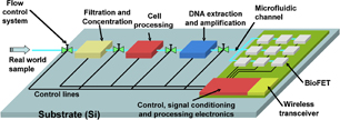
Fig. 2. Example of a biosensing system for the detection of pathogens in water using DNA hybridization.
Download figure:
Standard image High-resolution imageAs shown, the biosensing system includes control, signal conditioning and signal processing electronics54–57) to improve the quality of sensed signal. It also includes a low-power, low-cost silicon-based wireless transceiver58–62) to send information from the sensing environment (e.g., a rural area) to an urban center where appropriate actions can be taken if pathogens are present in the water sample. As shown, different material systems such as glass, various types of polymers, metals, silicon, gallium arsenide or indium phosphide are required to be bonded onto a common substrate. The nanobonding technologies discussed above is being developed for applications such as this and the one immediately below in Fig. 3 for bioimaging. More details on various components of this biosensing system can be found in our previous articles.45,47,63–65)
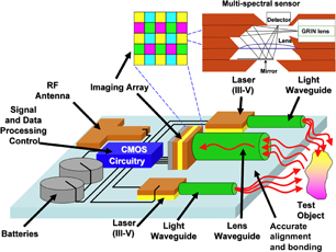
Fig. 3. Example of a bioimaging system for the detection of autofluorescence signatures for disease detection.
Download figure:
Standard image High-resolution imageFigure 3 shows an optical bioimaging system that is being developed to detect autofluorescent signatures from tissues,64,65) for example. One application we are pursuing is autofluorescence spectral and lifetime signatures of tissues from the gastrointestinal tract during a normal endoscopic or colonoscopic examination. These signatures, when matched to templates in a database, can be a screening and diagnostic tool for early detection of diseases. We have already developed compact concave gratings for spectral wavelength separation and focusing,66,67) several types high-speed, high-sensitivity photodiodes and imagers67–75) and optical coupling systems.74,75) We have also developed data and signal processing electronics.54–57) These individual components or systems, together with others being developed (such as lasers, and antennas), in diverse technologies (silicon, GaAs, InP, glass or polymer, etc.) must be integrated and bonded to create compact, high-performance bioimaging systems.67,74–79) It is such technologies that nanobonding technologies are expected to play a critical role. In the next section, we provide details on the preparation and characterization of samples from nanobonding experiments.
4. Specimen preparation and characterization
As received wafers were used for the surface characterizations and bonding experiments. No chemical treatments or processing were used, unless otherwise mentioned. For nanobonding, a number of custom designed bonders have been developed that allow for bonding in UHV,19) low vacuum20) and air.15) Before bonding, the contact angle and surface roughness of the non-activated and activated surfaces were investigated. The sessile drop method was used to determine the contact angle with a deionized (DI) water droplet (9 µL), using a Kruss DSA100. The surface roughness was measured with an atomic force microscope (AFM) from Veeco (ICON). For interfacial characterization, the bonding strength, nanostructure and current–voltage (I–V) characteristics of the bonded interfaces were examined. To measure the bonding strength, a tensile pulling tester from Instron was used. Scanning electron microscope (SEM) and high resolution transmission microscopy (HRTEM; JEOL JEM-2100F), were used to observe the micro- and nano-structure of the bonded interfaces. The I–V characteristics were measured using a semiconductor parameter analyzer (HP-4145B). Most experiments were carried out in the Micro- and Nano-Systems Laboratory (MNSL) at McMaster University.
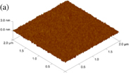
Figures 4(a) and 4(b) show a typical example for the AFM images of a Si surface before and after activation. The surfaces were homogeneously activated over the entire 2-in. diameter wafer by placing the activation sources at 45° with respect to the center of the specimens.19) All the specimens for nanobonding in UHV were activated with a 1.5 keV Ar-FAB source using 48 mA for 300 s, unless otherwise mentioned. Smooth surfaces were observed before and after activation. While the root mean square (RMS) surface roughness of Si before activation was 0.17 nm, it decreased to 0.11 nm after activation. Hence, the clean and smooth surfaces, that are required for the nanobonding of diverse wafers, were maintained or improved after activation.
Download figure:
Standard image High-resolution image
Fig. 4. AFM images of Si surface (a) before and (b) after surface activation.21)
Download figure:
Standard image High-resolution image5. Nanobonding results and discussion
5.1. Si/GaAs
Nanobonding in UHV requires thin wafers with low surface roughness. These parameters ensure intimate contact between the wafers to be bonded. In general, optically mirror-polished wafers provide nanometer-scale contact between the wafers. This intimate contact between two surfaces properly cleaned by using an Ar-fast atom beam in UHV can result in enhanced adhesion.
Figure 5(a) shows the infrared (IR) transmission images of the interfaces of Si/GaAs bonded using the nanobonding technology in UHV at room temperature.24) A number of voids were observed at the interfaces due to the presence of particles and other defects (e.g., metals ions) on the activated surfaces. The white and broken areas at the edges of the Si/GaAs bonded wafers are a result of the blade test. The blade test was performed in order to measure the bonding strength of the wafers. The insertion of the blade at the bonded interface failed due to the high bonding strength of the Si/GaAs substrates. Figure 5(b) shows the fracture image of Si/GaAs interfaces after the tensile pulling test.24) Bulk fractured GaAs remained on Si. The bonding strength of Si/GaAs was 14.4 MPa. This behavior shows that the bonded interface is not debonded during or after polishing. In general, the bonding strength depends on the weaker wafer of the bonded pair. Therefore, the relatively lower bonding strength of Si/GaAs24) than that of Si/Si21) can be due to the weaker fracture strength of the GaAs bulk material.

Fig. 5. (a) IR transmission image (b) fracture image, (c) HRTEM image, and (d) I–V characteristics of the p-Si/n-GaAs bonded interface. The specimens were bonded by using the nanobonding technology in UHV at room temperature.24)
Download figure:
Standard image High-resolution imageFigure 5(c) shows the HRTEM image of the interface of bonded Si/GaAs wafers.24) The thickness of the interfacial amorphous layer was 11.5 nm. The amorphous layer produced was due to the distortion of the lattice sites of Si and GaAs by the current of Ar-FAB.17,21–25,27) This amorphous layer is in contrast to that in the hydrophilic and hydrophobic bonding methods. The interfacial layer in these methods contains hydroxyl/oxide and hydrogen bonds, respectively.21,27,37) Therefore, the nanobonding in UHV is a covalent bonding rather than chemical reactivity of hydroxyl/oxide and hydrogen bonds in the hydrophilic and hydrophobic bonding.21,27)
Figure 5(d) shows the I–V behavior of p-Si/n-GaAs bonded wafers. The resistivity of the p-Si and n-GaAs were (0.01–0.02) and (2.2–2.3) × 10−3 Ω·cm, respectively. The electrodes for Si and GaAs were made by deposition of Au and Au/Ge with 3 mm diameter before bonding for the ohmic contacts. A non-typical I–V curve of the p–n junction was observed. However, analysis of the ideality factor of the junction using thermionic emission theory showed that the ideality factor of p-Si/n-GaAs was about 3.0.17,80) The electrical transport mechanism of Si/GaAs may be affected by the interfacial amorphous layer between Si and GaAs. The properties of this interfacial layer are most likely determined by the activation energy and time.17) The influence of activation parameters such as the Ar-FAB energy and activation time on the current density of the p–n junction was observed, as well as the influence of the exposure time in the UHV atmosphere.17)
5.2. Ge/GaAs
We have reported heterogeneous semiconductor wafer bonding of p-Ge/p-GaAs using nanobonding technology in UHV at room temperature.81) The dopants for Ge and GaAs wafers were gallium and zinc, respectively. The doping concentrations for both wafers were 1018 cm−3. Surfaces of Ge and GaAs wafers with RMS roughness of 0.25 and 0.48 nm,81) respectively, were simultaneously activated using two Ar-FABs. The vacuum pressure of the chamber was ∼6 × 10⁻⁶ Pa. The energy and current of the FAB was 1.1 keV and 100 mA, respectively. The activated wafer surfaces were contacted with an applied load of 1960 N for 2 min at room temperature.
Figures 6(a) and 6(b) show the scanning acoustic microscope (SAM) images of the Ge/GaAs nanobonded interfaces before and after annealing, respectively. The annealing was done in nitrogen at 250 °C for 2 h. Before annealing, the bonded interface showed a number of voids. These voids were annealed out.81) The mechanisms responsible for the behavior of the interfacial voids before and after annealing have not been studied in detail as yet. In fact, the SAM result of the nanobonded Ge/GaAs interface is different from the IR images of that of Si/Si.21) This difference of the nanobonded interfaces will be investigated using SAM. On the other hand, the bonding strength measured by tensile pulling test was 4.87 MPa. The bonding strength of Ge/GaAs is lower compared to Si/Si.21) The low bonding strength may be due to the (1) high surface roughness of GaAs after surface activation, and (2) voids at the interface. Also, the external load for bonding and the hardness31) of Ge and GaAs may influence on the bonding strength.
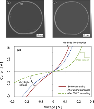
Fig. 6. SAM images of the Ge/GaAs nanobonded interfaces (a) before and (b) after annealing in nitrogen at 250 °C. (c) I–V characteristics of p-Ge/p-GaAs before and after annealing at 250 and 350 °C.81)
Download figure:
Standard image High-resolution imageFigure 6(c) shows the I–V characteristics of p-Ge/p-GaAs before and after annealing at 250 and 350 °C. The electrical behavior is not the typical diode-like characteristics. However, this behavior is similar to that in p-Si/p-Si,21) n-GaAs/n-GaAs,82) n-Si/n-GaAs.82) Surface damage during activation may cause this behavior. After annealing, the current between p-Ge and p-GaAs decreased. The decreased current may be due to the oxidation of Ge and GaAs. We have observed identical behavior at the nanobonded Si/Si interface. We demonstrated that the electrical current of Si/Si was increased with the annealing temperature after subtracting the influence of thermal oxides of Si.21) Also, we observed that the amorphous layer of the bonded interface was converted into a crystalline one with the annealing temperature and the surface damages caused by activation were annihilated.21)
5.3. Si/glass
In contrast to nanobonding in UHV, chemical reactivity of the surface controls the spontaneity in the nanobonding in air. The reactivity is controlled by the roughness and water contact angle of the surface.83) Table II summarizes the roughness and water contact angle of the surface of Si, SiO2 (the SiO2 was a 50 nm thick thermal oxide on Si), Ge, GaAs, and glass (500 ± 25 µm thick Pyrex 7740 borosilicate) before and after sequential plasma activation.15,16,21,83) The sequential plasma activation refers to the two step surface cleaning using an RF-RIE plasma and MW neutral radicals.20,38–40)
Table II. Summary of surface roughness and water contact angle of specimens including plasma processing parameters for surface activation used in the nanobonding in air.15,16,83)
| Specimen | Surface activation O2 RF (OR) and N2 MW (NM) plasma (kW), time (t) (s), pressure (P) (Pa) | RMS surface roughness (nm) | Contact angle (°) |
|---|---|---|---|
| Si | Without | 0.17 | 33.4 |
| 0.2 (OR), 30 (t), 60 (P); 2.0 (NM), 30 (t), 60 (P) | 0.14 | 20.4 | |
| 0.05 (OR), 15 (t), 60 (P); 2.5 (NM), 30 (t), 60 (P) | 0.16 | 22.5 | |
| SiO2 | Without | 0.14 | 52.0 |
| 0.2 (OR), 30 (t), 60 (P); 2.0 (NM), 30 (t), 60 (P) | 0.12 | 34.2 | |
| Ge | Without | 0.25 | 68.0 |
| 0.2 (OR), 30 (t), 60 (P); 2.0 (NM), 30 (t), 60 (P) | 0.18 | <2 | |
| 0.05 (OR), 15 (t), 60 (P); 2.5 (NM), 30 (t), 60 (P) | 0.20 | <2 | |
| GaAs | Without | 0.18 | 77.0 |
| 0.05 (OR), 15 (t), 60 (P); 2.5 (NM), 30 (t), 60 (P) | 0.13 | <2 | |
| Glass | Without | 0.52 | 29.0 |
| 0.05 (OR), 15 (t), 60 (P); 2.5 (NM), 30 (t), 60 (P) | 0.46 | 17.7 |
Some processing parameters such as power, time and pressure of the plasma here provide a proper surface so nanobonding can take place. Before surface activation, the RMS surface roughness of Si, SiO2, Ge, GaAs, and glass was 0.17, 0.14, 0.25, 0.18, and 0.52 nm, respectively. This variation in the surface roughness indicates different level of sensitivity of the surface elements. The nature of the chemical mechanical polishing step during surface preparation controls the roughness. This step is critical for glass surface because of the presence of the alkaline and silicate elements.15)
The water contact angles of Si, SiO2, Ge, GaAs, and glass before surface activation were 33.4, 52.0, 68.0, 77.0, and 29.0°, respectively. After surface activation, the contact angle decreased considerably for all surfaces. The decrease in the contact angle increases the surface energy and thereby enhances the chemical reactivity of the surface.83) The decrease in the contact angle was significant for Ge and GaAs surfaces. The contact angle was less than 2° which is below the detection limit of the DSA. This very low contact angle is due to the termination of large amount of hydroxyl molecules on the free-dangling sites of plasma cleaned Ge and GaAs surfaces when exposed to the clean room ambient.83) However, a simple analytic relationship between the surface roughness and the contact angle was not observed.
Figure 7(a) shows the optical image of glass/Si wafers bonded by the sequential plasma activation followed by anodic bonding at 200 °C with the anodic voltage of 1 kV.15) This process is known as hybrid plasma bonding (HPB). While the voids were observed at the interface in the sequential plasma activated bonding (SPAB), the void-free interfaces were achieved by using HPB. In HPB, voids were absorbed in the interfacial oxide.15) The absorption of the voids depends on the thickness of the oxide. However, the voids due to the presence of particles on the activated surface and plasma induced surface defects that trap air at the interface could not be removed. Therefore, HPB provides a nearly void-free interface by combining effect of electrostatic force and adhesion between the hydrophilic surfaces.15,16) Unfortunately, we have not yet investigated HPB for hydrophobic surfaces. Figure 7(b) shows the fracture images of bonded glass/Si wafers in SPAB and HPB after tensile pulling tests.15) The left image indicates a partial fracture of glass in SPAB. The right image shows a complete fracture of glass after HPB at 200 °C. That is, while fractures at the interface and bulk materials of Si and glass were observed in the SPAB, fractures only in the bulk material of glass were observed in the HPB. This indicates stronger bonding strength in the HPB than that in the SPAB.15) Figure 7(c) shows the HRTEM images of the hybrid plasma bonded interfaces of Si/glass.15) The HRTEM images show the presence of intermediate amorphous layers at the bonded interfaces. The thickness of the interfacial amorphous layer was ∼353 nm. The amorphous layer was brighter than bulk glass and Si, which was a sodium depletion region identified by using energy dispersive X-ray analysis.84) The higher brightness was due to the smaller mean atomic number of the depletion region compared to that of the bulk glass, caused by the migration of sodium and potassium cations.85) A dark band was observed at the interface of Si/glass. The dark band at the edge of depletion region in glass was attributed to the accumulation of less mobile potassium cations.85)
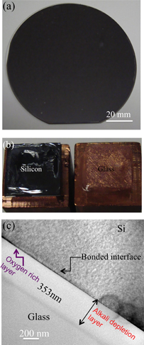
Fig. 7. Images of (a) optical (b) fracture and (c) HRTEM of Si/glass interface bonded by hybrid plasma bonding at 200 °C and 1 kV for 10 min.15)
Download figure:
Standard image High-resolution imageFigure 8 shows a comparative study of the bonding strength of Si/Si, glass/glass, Si/Ge, SiO2/Ge, Si/glass, Ge/glass, and GaAs/glass bonded wafers with different bonding conditions. The activation parameters for the specimens are given in Table II. The activation parameters for all the specimens are identical except the energy of O2 RIE plasma for the GaAs and Glass wafers. Also, the surface roughness of glass is higher than that of other wafers. Furthermore, while the water contact angles of Ge and GaAs before the activation are in the ranges of 70°, surface activation changes them into the values that are below the detection limit of the water contact angle measurement equipment (i.e., DSA100).

Fig. 8. Bonding strength of Si/Si, glass/glass, Si/Ge, SiO2/Ge, Si/glass, Ge/glass, and GaAs/glass bonded wafers. The specimens of Si/Si and glass/glass were bonded by using the SPAB at room temperature. The specimens of Si/Ge and SiO2/Ge were bonded by using the SPAB and were heated at 200 °C for 4 h. The specimens of Si/glass, Ge/glass, and GaAs/glass were bonded by using hybrid plasma bonding at 200 °C and 1 kV for 10 min.15,16,41,83,86)
Download figure:
Standard image High-resolution imageSubstrates of Si/Si and glass/glass were bonded using SPAB at room temperature.41,86) Si/Si and glass/glass were not heated because heating does not improve the bonding strength in SPAB due to the formation of voids at the bonded interface.21,41,86–88) The specimens of Si/Ge and SiO2/Ge were bonded by using SPAB and were heated at 200 °C for 4 h.83)
The specimens of Si/glass, Ge/glass, and GaAs/glass were bonded by using HPB at 200 °C and 1 kV for 10 min.15,16,83) The bonding strength of Si/glass is the highest compared to all other wafers. This is as a result of highly hydrophilic, reactive, and smooth surfaces of Si and glass after sequential plasma activation. Si/Si and glass/glass wafers, after Si/glass, offer high bonding strength at room temperature. It is worth noting that while the Si and glass surfaces have identical hydrophilicilty, that is the high reactivity and smooth surfaces in both the SPAB and HPB methods, why the Si/glass bonded interface in HPB shows the highest bonding strength. The highest bonding strength in HPB is due to the formation of an alkaline depletion layer in the glass and an amorphous SiO2 interface that is shared by the bonded wafers. These phenomena are attributed to the opposite migration of alkaline cations and anions between the contacted wafers under the applied voltage at an elevated temperature.15,87,88) The bonded interface in SPAB does not provide to these phenomena21,41,86) that results in high bonding strength.
The bonding strength of Si/Ge was the lowest. This is due to the high reactivity of Ge wafer after surface activation. The activated surface is terminated by hydroxyl molecules when exposed to the clean room ambient. The hydroxyl molecules result in low water contact angle of less than 2° which remains unchanged after 2 min of the measurements. This low water contact angle indicates a large number of OH− molecules at the Ge activated interface. Therefore, the high reactivity is responsible for the weak bonding strength of Si/Ge. After heating at 200 °C, the bonding strength of Si/Ge was slightly improved, but this temperature was still not sufficient to remove the OH− molecules. Identical results on the weak bonding strength of Si/Ge were reported89) due to the enhanced surface oxidation induced by the oxygen and nitrogen radicals. The bonded wafers were annealed at 200 °C for 24 h, and additionally at 300 °C for 24 h to improve the bonding strength.89)
The relatively high bonding strength of glass/Ge is due to the increase in surface energy (i.e., low water contact angle) after surface activation38) of glass. Higher reactivity difference of SiO2/Ge wafers is again due to the unique reactivity of Ge, as well as the water absorption of SiO2 layer. Annealing at 200 °C offers higher boding strength in SiO2/Ge compared to that in Si/Ge. The bonding strength of Si/Ge and SiO2/Ge in SPAB after annealing at 200 °C was lower than that of Si/Si and glass/glass in SPAB at room temperature. As previously mentioned, this relatively low bonding strength in the Si/Ge and SiO2/Ge can be attributed to the high reactivity of activated Ge wafer after being exposed to air. This phenomenon is in contrast to that in the nanobonding of Si/Si and glass/glass in UHV that results strong covalent bonding at room temperature.15,16,21,83) In HPB, the difference in bonding strengths of Si/glass, Ge/glass, and GaAs/glass is due to the difference in the widths of the depletion layer at the interface and the strengths of the bulk materials of Si, Ge, and GaAs wafers. Thicker depletion layer at the interface, and weaker strength of materials results in lower bonding strength and vice-versa.15,16,21,83)
5.4. Cu-through silicon vias/Au-stud bumps
The copper-through silicon vias (Cu-TSVs) and gold-stud bumps (Au-SBs) nanobonding was accomplished in UHV after surface activation with a 1.5 keV Ar-FAB using 48 mA for 300 s at room temperature. While the Au-SBs have been used in microelectronics packaging for a long time, high-density interconnection between Cu-TSVs and Au-SBs through nanobonding can be used in the miniaturized biosensing and bioimaging systems.45,90) The shape of the top surface of stud bumps does not allow for nanobonding. Therefore, a low cost solution has been utilized to flatten the top surface of the stud bumps by applying an external compressive pressure of about 81.5 MPa over each bump (external force 0.16 N/bump) on this surface.90) This process improved the surface roughness and contact area that required for the nanobonding.
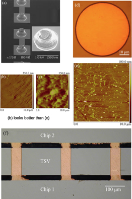
The first three figures in Fig. 9 show the scanning electron microscope images of the flattened Au-stud bumps [Fig. 9(a)]; the AFM images of Au-stud bump surface over 10 × 10 µm2 of deformed (flattened by using the external force) [Fig. 9(b)] and non-deformed (not-flattened) [Fig. 9(c)] areas, respectively. Figure 9(d) shows the optical image of Cu-TSV wafer and Fig. 9(e) shows the AFM image of Cu-TSV surface over 10 × 10 µm2 of area. Figure 9(f) shows the optical image of the cross-section of Au-SB/Cu-TSV. The base and height of the Au-SBs were 50 and 37 µm, respectively. The Au-SBs were flattened using an external compressive pressure about 81.5 MPa over each bump to improve the surface roughness. A number of Cu-TSVs (120) were vertically sandwiched between two chips with Au-SBs. The RMS surface roughness of the deformed area was 9.6 nm, which is significantly improved compared with that of non-deformed area (36.1 nm). Through AFM investigations of TSV surface over 10 × 10 µm2 of area in Fig. 9(e), the surface roughness was measured to be 6 nm. Since this surface roughness of deformed Au-SBs and Cu-TSVs does not fully meet the requirement of nanobonding in UHV,19) a 20 N external force was applied for bonding at room temperature. The estimated applied pressure was about 81.5 MPa (i.e., 0.16 N/bump area). Here the base of the bumps (i.e., 50 µm) was used for the calculation of the bump area. After bonding, no considerable misalignment is observed in the cross-sectional view of the bonded Au stud bumps and Cu-TSV, as shown in Fig. 9(f). In addition, the bonding strength of Au-SB and Cu-TSV was approximately as high as 110 MPa.90)
Fig. 9. (a) SEM images of the flattened Au-stud bumps; AFM images of Au-stud bump surface over 10 × 10 µm2 of (b) deformed and (c) non-deformed areas; (d) optical image of Cu-TSV; (e) AFM image of Cu-TSV surface over 10 × 10 µm2 of area; and (f) cross-sectional optical image of vertically integrated Au-SB/Cu-TSV interfaces.90)
Download figure:
Standard image High-resolution image
The electrical resistance of the interconnect, which includes two interfaces between Au-SB and Cu-TSV and the height of one Cu-TSV, was only 0.5 Ω.90) A mechanical caulking technique has been reported to bond Au-SBs with TSVs at room temperature to achieve three-dimensional (3D) assembly by applying compressive pressure to squeeze the former into the latter.5) The compressive pressure is about 815 MPa,5) which is about one order higher than that of the pressure used in this work.90)
5.5. Chemical/vapor assisted nanobonding
Further modification in the surface preparation for nanobonding has been realized in order to address the prolonged activation time issue for some materials such as Cu. In general, a Cu surface contains 10–20 nm thick oxides. The surface activation of Cu using Ar-FAB for the nanobonding requires prolonged etching time due to the thick oxides.29) The prolonged activation results in a rough surface and causes failure of Cu/Cu bonding in the UHV. Therefore, it is very difficult to remove copper oxides and achieve high quality of nanobonding of Cu/Cu. On the other hand, the ambient for surface activation of semiconductors, such as Si and GaAs is critical in the first category of nanobonding if UHV is not maintained. Many of the combinations of the semiconductors do not bond without UHV. To address these issues, a new modified method of the nanobonding has been developed.91–93) It is known as chemically assisted nanobonding. In this method, the Cu surfaces were treated using formic acid gas for surface activation. Formic acid gas was generated using N2 gas bubbling through a bottle having a solution of formic acid. The treatment of Cu with formic gas reduces its oxide. The X-ray photoelectron spectroscopy spectra showed that 9 min of formic acid gas activation completely removed hydroxide, oxides and organic contaminations from the Cu surface.91,93) Therefore, the chemically assisted activated surfaces of Cu can be bonded at a temperature below 200 °C.91–93)
In another study, water vapor was used to bond various combinations of bumpless Cu structures, SiO2, and polyimide.94) The motivation in this modified method is identical to that in the third category of nanobonding. It is to create hydroxyl groups on the surface after activation. In the vapor-assisted nanobonding,94) the smooth surfaces were activated with an Ar-FAB source using 1.5 kV and 15 mA for 180 s, followed by exposure to the nitrogen atmosphere containing water vapor of various absolute humidities for 600 s. The pressure for exposing nitrogen gas was 9 × 10⁴ Pa (0.89 atm). Cu surface was changed into Cu hydroxide. On the other hand, the surfaces of SiO2 and polyimide were terminated with silanol and hydroxyl groups. Finally these surfaces were mated at RT and then heated at 150 °C for 600 s.94) The newly grown and terminated layers resulted in strong adhesion after heating. The bonded interface of Cu/Cu had an electrical resistivity of 4 × 10⁻⁸ Ω·m.94)
6. Conclusions and future perspectives
Four types of surface-activated nanobonding have been developed to address the heterogeneous integration challenges for "More than Moore". The nanobonding techniques offer nanometer scale bonding through direct contact between smooth surfaces. Therefore surface preparation is one of the key parameters which control the quality of the bonded interface. The bonding quality is also dependent on the sensitivity of the surfaces to activation source, bonding atmosphere and external force.
Nanobonding in ultrahigh vacuum (UHV) has been performed at room temperature for heterogeneous integration of semiconductors, such as Si/GaAs, Ge/GaAs, and Si/glass. Void-free, strong, and atomic-scale bonding was confirmed. The I–V behavior of the nanobonded p–n junction of the semiconductors was leaky. Investigation on controlling activation parameters, such as voltage, current and power of the sources is needed to achieve typical p–n junction behavior.
An example of nanobonding of metallic materials using Cu through silicon vias (Cu-TSV)/Au-stud bumps (Au-SBs) in UHV has been demonstrated. Cu-TSVs have been vertically integrated between chips with Au-SBs for 3D integration at room temperature. High bond strength was identified at the Cu/Au interface.
For nanobonding in air at room temperature, a sequential plasma activated bonding (SPAB) technique has been developed. The O2 RIE plasma followed by MW N2 radicals was used for the sequential plasma activation. For nanobonding of ionic materials, the sequentially activated semiconductors and glass were bonded under anodic treatment at 200 °C, known as the hybrid plasma bonding (HPB) technique. Void-free, strong and nanometer scale bonding of diverse materials in HPB were observed.
Further modification in the surface preparation for nanobonding was needed to address the activation challenges of surfaces with thick oxide, such as Cu surface. This newly modified nanobonding utilizes chemical/vapor to ease the thick oxide issues. Prior to the activation of Cu surfaces, formic acid gas was used to reduce the Cu-oxide. These chemically assisted activated surfaces of Cu were bonded at 200 °C. Also, water vapor assisted different combinations of bumpless Cu structures, SiO2, and polyimide were bonded at 150 °C. Therefore, the heterogeneous integration capabilities of the nanobonding technologies may have significant potential and opportunities in the development of the biosensing and bioimaging systems for emerging applications in health and environmental sciences.
Acknowledgments
This research is supported by Discovery Grants from the Natural Science and Engineering Research Council of Canada, an infrastructure grant from the Canada Foundation for Innovation, an Ontario Research Fund for Research Excellence Funding Grant, a FedDev of Southern Ontario grant and the Canada Research Chair program.
Biographies

Matiar M. R. Howlader received a B.Sc. Eng. degree in Electrical and Electronic Engineering from Khulna University of Engineering and Technology, in Khulna, Bangladesh, in 1988, and his M.S. and Ph.D. degrees in Nuclear Engineering from Kyushu University, Fukuoka, Japan, in 1996 and 1999, respectively. Currently, Dr. Howlader is leading the nanobonding and packaging research group in the Department of Electrical and Computer Engineering at McMaster University, Hamilton, ON, Canada. His research focuses on the nano-integration of bio-micro-opto-electromechanical systems and implantable systems for health and environmental applications.

M. Jamal Deen received the Ph.D. degree in electrical engineering and applied physics from Case Western Reserve University, Cleveland, OH, in 1985. His Ph.D. dissertation was focused on the design and modeling of a new CARS spectrometer for dynamic temperature measurements and combustion optimization in rocket and jet engines, and was sponsored and used by NASA, Cleveland. He is currently a Professor of Electrical and Computer Engineering, Senior Canada Research Chair in Information Technology and Director of the Micro- and Nano-Systems Lab-oratory at McMaster University. His research interests include nanoelectronics, optoelectronics, and nanotechnology and their emerging applications for health and environmental sciences.

Tadatomo Suga received the M.S. degree in precision engineering from the University of Tokyo, Tokyo, Japan, in 1979, and the Ph.D. degree from the Max-Planck Institut für Metallforschung, University of Stuttgart, Stuttgart, Germany, in 1983. His Ph.D. thesis was focused on fracture mechanics characterization of metal–ceramic interfaces. He is currently a Professor of Precision Engineering at The University of Tokyo. He is a Director with a Research Group, National Institute of Materials Science, Tsukuba, and also a member of the Science Council of Japan. His current research interests include microsystems integration and packaging using room temperature bonding method for various applications.