
Abstract
First, the experimental implementations and theoretical/numerical investigations of surface plasmon (SP) coupled InGaN/GaN quantum-well light-emitting diodes (LEDs) are reviewed. If the p-GaN layer in an LED can be thin, surface metal nanoparticle (NP) is an inexpensive structure for inducing effective SP coupling. When the p-GaN layer is thick, a few metal structures, including metal protrusion, buried metal NP, and embedded metal NP, can be used for effective SP coupling. In the numerical study, an algorithm, including the feedback effect of the induced SP resonance on the radiating behavior of the source dipole, has been proposed for studying the SP coupling effects with an embedded metal NP, a surface metal NP, and a metal protrusion. Then, the theoretical formulations and numerical algorithms for evaluating the radiated power enhancement in the coupling process between two radiating dipoles and the localized surface plasmon (LSP) induced on a nearby Ag NP are built. Three mechanisms are considered in the coupling process for radiated power enhancement, including the interference of the two phase-retarded radiation contributions from the two dipoles, the interaction between the two dipoles, and the LSP resonant coupling.
Export citation and abstract BibTeX RIS
1. Introduction: Mechanism of surface plasmon coupling
When an electromagnetic wave interacts with a metal nanoparticle (NP) or a metal/dielectric interface at an appropriate frequency, the resonance of a surface plasmon (SP), either localized surface plasmon (LSP) or surface plasmon polariton (SPP), can be induced for producing a strong electric field in the vicinity of the metal structure.1) SP coupling with a light emitter for enhancing its emission efficiency is an attractive research topic due to its important application to the performance improvement of a light-emitting device. When a light emitter or radiating dipole is placed near a metal NP or a metal/dielectric interface, the induced SP can couple with the dipole and enhance the overall emission efficiency because such a coupling process can increase the radiative transition rate of a radiating dipole.2–5) Such an SP coupling mechanism has been applied to an InGaN/GaN quantum-well (QW) light-emitting diode (LED) for enhancing its overall emission efficiency. It has also been used for increasing the light extraction efficiency of an organic light-emitting device.6,7) Although the SP coupling process has been widely used, its physical insides are still not completely clear.
The emission efficiency enhancement of a radiating dipole near a metal NP or a metal/dielectric interface can be interpreted with the Purcell effect, in which the near-field distribution of an SP mode around the metal structure is regarded as an effective resonance cavity.8) When a radiating dipole is placed in such a resonance cavity, its emission efficiency can be enhanced by the Purcell factor. The coupling process between an SP mode and a radiating dipole is similar to the mechanism of stimulated or amplified spontaneous emission in a laser system. Such a coupling mechanism can be regarded as a process of amplifying the near field of the SP mode by a gain medium, which includes the radiating dipole. In other words, the radiating dipole transfers energy into the SP mode for emission. With the coupling between the SP mode and the radiating dipole, they emit light together coherently. Figures 1(a) and 1(b) show schematically the top portion of a lateral QW LED with a metal layer and a metal NP, respectively, on the top of the p-GaN layer. When an SP mode is induced at the metal/GaN interface or on the metal NP by the spontaneous emission of the radiating dipoles in the QW, it extends an evanescent or a near field distribution into the p-GaN layer, as depicted by the red curve in either Fig. 1(a) or 1(b). If the p-GaN layer is reasonably thin, the evanescent or near field distribution can cover the QW. In this situation, the carrier energy in the QW can be transferred into the SP mode for radiation through the amplification of the evanescent or near field by the excited QW. Therefore, the SP coupling creates an alternative emission channel besides the intrinsic emission through carrier recombination. It is noted that because an SP mode loses energy through metal dissipation, the SP coupling process also creates a new energy loss channel. Therefore, we can obtain an effective emission efficiency enhancement only when the new loss channel is weaker than the intrinsic energy loss in the QW, i.e., non-radiative recombination of carriers in the QW. The metal layer on the top of the p-GaN layer shown in Fig. 1(a) can be used for inducing SPP coupling with the QW. The metal NP shown in Fig. 1(b) can be used for inducing LSP coupling with the QW. However, it is noted that besides a metal NP, LSP resonance for QW coupling can be induced in a nanostructure on a metal thin film, such as a nano-bump or a nano-depression.
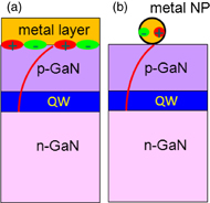
Fig. 1. Schematic demonstration of the top portion of a lateral QW LED with a metal layer (a) or a metal NP (b) on the top of the p-GaN layer for inducing SP coupling. The (red) curves depict the near field distributions of SP modes.
Download figure:
Standard image High-resolution imageIn a QW light-emitting device, there are many radiating dipoles in a QW. When a metal NP or a metal/dielectric interface is placed near the QW, an induced SP mode can possibly couple with all the radiating dipoles within the near field distribution range of the SP mode. In this situation, the coupled dipoles can emit coherently together with the SP mode, leading to stronger emission intensity, when compared with the superposition of the incoherent emissions of individual dipoles. Such a coherent emission behavior can make a light-emitting device become a localized coherent light source, which is expected to have higher emission efficiency. Although the coupling of an SP mode with a radiating dipole has been theoretically and numerically studied, so far, the coupling between an SP mode and multiple radiating dipoles has not been properly investigated yet.9–12)
In the first part of this paper, we review the experimental studies on SP coupled InGaN/GaN QW LED and the related theoretical/numerical investigations. This review starts with the discussions of several important issues in designing the structure of an SP-coupled LED (in Sect. 2.1). Then, the fabrications and characterization results of SP-coupled LEDs reported in literature are reviewed (in Sect. 2.2). Next, the related theoretical/numerical studies on the SP coupling with a radiating dipole are discussed (in Sect. 2.3). In the second part of this paper, we present the numerical investigation results of the coupling process of an LSP resonance mode induced on a metal NP with two radiating dipoles to show the coherent emission behaviors of the system consisting of the metal NP and two radiating dipoles. This part of presentation consists of the review of the emission behaviors of a two-dipole system (in Sect. 3.1), the descriptions of the problem geometry and used numerical method (in Sect. 3.2), the report of the numerical results (in Sect. 3.3), the discussions of the numerical results (in Sect. 3.4), and the summary of this numerical investigation. Finally, the overall conclusions of this paper are drawn in Sect. 4.
2. Review of SP coupled LED
2.1. Issues in implementing SP coupled LED
The SP coupling with a QW of an LED can lead to the following advantages. First, due to the creation of the alternative emission channel, the effective internal quantum efficiency (IQE) of the QW can be enhanced.13) Second, because of the change of radiation pattern after the radiating dipoles in the QW couple with SP modes, the light extraction efficiency of an LED can be increased.14) Third, during the coupling process, the carrier energy is effectively transferred into the SP mode such that the carrier density in the QW can be maintained at a low level. In this situation, the efficiency droop effect can be reduced.13,15) Although the physical mechanism for the efficiency droop effect is still controversial, basically it is caused by the high carrier density in the QW when injection current is large. Therefore, the transfer of carrier energy into the SP mode for decreasing the carrier density can reduce the efficiency droop effect. Fourth, when the metal for inducing SP modes has an anisotropic structure, such as a one-dimensional metal grating, the LED output becomes partially polarized due to the polarized SP coupling behavior.13,16,17) Fifth, because of the stimulated emission nature in SP coupling, the device response to frequency modulation is enhanced such that the modulation frequency of an SP-coupled LED can be increased. This behavior is important for the application of visible communications. Sixth, as mentioned in Sect. 1, an SP mode can couple with more than one radiating dipole. In this situation, those coupled dipoles emit light coherently, leading to partially coherent emission and relatively higher intensity from the LED. This issue will be further discussed in Sect. 3. Finally, because part of carrier energy is transferred into an SP mode, the energy loss originally through non-radiative recombination is reduced. Although part of transferred energy becomes loss through metal dissipation, this part of loss produces heat in the surface metal, instead of heat in the QW. It is easier to remove the heat in the surface metal, when compared with that in the QW. Therefore, SP coupling can reduce LED device heating.
In designing an SP-coupled LED, the following criteria need to be considered. (1) The SP resonance wavelength needs to match with the QW emission wavelength for maximizing the coupling strength. The SP resonance wavelength is affected by several factors, including metal material, metal geometry, excitation source location, and the refractive index of the surrounding material. Therefore, quite many parameters can be adjusted for controlling the SP resonance wavelength. (2) The distance between the QW and the metal structure, particularly the metal portion producing a strong near field distribution for SP coupling, needs to be reasonably small. This distance has been considered as the most important issue in designing an SP-coupled LED. Usually, it is believed that the distance must be smaller than the decay range of the near field distribution of the SP mode. This decay range is around 50 nm in GaN for an Ag structure surrounded by or contacting GaN. However, as to be discussed in Sect. 2.3, the distance for effective SP coupling can be larger than this value (up to 100 nm). The condition of a small distance between the metal structure and QW implies the requirement of a thin p-GaN layer in an LED. In this situation, current crowding in such a device becomes a problem. Therefore, the compromise between the SP coupling strength and the current spreading condition is an important issue in designing an SP-coupled LED. (3) It is better to use an SP mode with strong resonance and low metal loss for coupling with the QW. For this purpose, the metal structure needs to be carefully designed and the surrounding medium needs to be carefully chosen.
2.2. Experimental implementations
Photoluminescence (PL) measurement has been widely used for studying the SP coupling behaviors with an InGaN/GaN QW.3,18) However, with PL measurement, cautions need to be taken for making a reasonable comparison between an SP-coupled sample and a control sample of no SP coupling effect, including the accuracy of PL signal collection, the variation of the excitation intensity at the QW after a metal structure is added to the sample, and the temperature-dependent behavior of the metal structure. In the review as follows, we will focus on the implementations of SP-coupled LED. In implementing an SP-coupled LED, the evidence of SP coupling is needed besides the observation of LED output enhancement because the output enhancement may be caused by other factors, such as the non-resonant scattering of the metal structure. A reliable approach for demonstrating the evidence of SP coupling is to fabricate LED samples of different distances between the metal structure and the QW for comparison. Among different noble metals used for SP generation, Ag has the lowest dissipation rate. Also, the spectral range of its SP resonance covers the visible window longer than ∼440 nm, which is the SPP resonance wavelength at an Ag/GaN interface. Compared with Ag, Au has a higher dissipation rate and a longer SP resonance wavelength.
Figure 2(a) schematically shows six metal structures, as denoted by A–F, for inducing SP coupling with the QW in a lateral LED. Figure 2(b) schematically shows a metal structure for inducing SP coupling with the QW in a vertical LED (structure G). In structure A, a metal film is coated on the p-GaN layer to form a smooth metal/GaN interface.15,19) At the interface, SPP can be induced for coupling with the radiating dipoles in the QW. Although SPP cannot interact with a plane wave unless a momentum compensation scheme is provided, it can interact with a nearby radiating dipole through near-field coupling. However, if the metal/GaN interface is rough or periodically grooved, the generated momentum compensation scheme can further enhance the total emission power. Structure B in Fig. 2(a) shows a metal grating structure on the p-GaN layer. For producing the momentum compensation effect, normally the grating period needs to be smaller than 200 nm for a green LED and even smaller for a blue LED. However, it is costly to fabricate such a short-period metal grating on GaN. With a larger period, LSP resonance can be formed within a period of the grating structure for coupling with the QW if the grating period and duty cycle are well designed.13,16,17) The simplest metal structure for inducing SP coupling is a surface metal NP array on the top of the p-GaN layer, as structure C in Fig. 2(a). The metal NPs can be fabricated through the thermal annealing of a thin metal film.20,21) In this situation, the size and position of metal NP are randomly distributed. Regularly arranged metal NPs of uniform size can be fabricated through nano-imprint lithography, dry etching, and liftoff process. Compared with the metal NPs of random nature, the spectral width of the LSP resonance feature is smaller and hence the resonance strength at the peak is stronger. However, with this technique, usually a conducting oxide material needs to be deposited on the top for protecting the metal NPs from being removed during the device process procedure and spreading injection current. In this situation, the LSP resonance wavelength can be red-shifted to become away from the designated QW emission wavelength. With those three metal structures (A–C), to increase the SP field strength at the QW, the thickness of the p-GaN layer needs to be small, usually smaller than 70 nm. In a standard lateral LED, including the top QW barrier layer of ∼10 nm, the p-AlGaN electron blocking layer [not shown in Figs. 1, 2(a), and 2(b)] of ∼20 nm, and the p-GaN layer of <70 nm, the distance between the metal structure and the top QW is <100 nm. This is roughly the distance limit of effective SP coupling. However, with such a thin p-GaN layer, usually the electrical property of an LED is poor. To improve the electrical property, other metal structures need to be designed with a thicker p-GaN layer.

Fig. 2. (a) Schematic demonstrations of six metal structures (A–F) for inducing SP coupling with the QW in a lateral LED. (b) Schematic demonstration of a metal structure (G) for inducing SP coupling with the QW in a vertical LED.
Download figure:
Standard image High-resolution imageWith a thick p-GaN layer, to make the distance between the metal structure and the QW short, we can fabricate a metal protrusion structure like structure D shown in Fig. 2(a).22) In a realization, on the 120-nm p-GaN layer, a triangularly patterned hole array is first fabricated with 120 nm in hole depth, 100 nm in hole diameter, and 200 nm in pitch. In this situation, the distance between the hole bottom and the last-grown QW is ∼30 nm, including the 20-nm p-AlGaN layer and a 10-nm QW barrier layer. Then, the holes are filled with Ag to form the structure of Ag protrusion. The ∼30-nm distance between the protrusion tip and the last-grown QW leads to a ∼75% enhancement of LED output intensity through the coupling of the LSP resonance field around the protrusion tip with the QW. The protrusion structure has the advantage of making the metal structure close to the QW while maintaining a thick p-GaN layer. However, because we need to use a dry etching process for fabricating the hole pattern, surface damage can be produced on the sidewall and bottom of a hole. Unless such damaged surface is carefully cleaned through a wet etching process, significant current leakage exists in such a device. Also, because the direct contact of Ag onto GaN may lead to high resistance, the current flow through Ag protrusion can degrade the electrical property of such a device. To solve this problem, with a liftoff process, we can form Ag NPs in the holes and cover the Ag NPs with SiO2 NPs through the immersion of the sample in a SiO2 solution. As schematically shown in structure E of Fig. 2(a), the SiO2 NPs can block the injected electric current from flowing through the Ag NPs. In this situation, the current leakage can be reduced. To make metal NPs close to the QW, an effective approach is to embed the metal NPs in the p-GaN or n-GaN layer [see structure F in Fig. 2(a) for metal NP embedment in the p-GaN layer].23–26) This approach involves the procedures of the coating of metal NPs on a sample of incomplete epitaxial growth and a regrowth process. It can make the distance between metal NPs and the QW very close. However, to guarantee high-quality regrowth, the planar metal coverage cannot be high. In this situation, the overall SP-coupling effect can be weak. Also, with the Ag or Au NPs completely surrounded by GaN, the major LSP resonance (dipole resonance) wavelength is red-shifted into the yellow-red range. Hence, for the application in the blue-green range, the SP coupling relies on weaker higher-order LSP resonance modes. Meanwhile, the required regrowth process makes the fabrication cost of such a device higher. Nevertheless, metal NP embedment represents the most effective method for reducing the distance between the metal structure and QW and hence enhancing the SP coupling effect. This approach deserves further investigation.
SP coupling can also be applied to a vertical LED. Figure 2(b) shows a design (structure G) with a metal grating formed between the p-GaN layer and the wafer-bonding metal.13) Such a metal grating does not necessarily provide us with a momentum compensation scheme for producing an effective coupling effect (a large emission enhancement) between an SPP mode and the QW. Instead, the grating serves as a periodical array of one-dimensional metal protrusion. Therefore, the LSP resonance mode with its field distribution around the protrusion tip can strongly couple with the QW. In an implementation, with ∼120 nm in p-GaN thickness, an Ag grating period of ∼520 nm and a groove depth of ∼65 nm can lead to an output intensity enhancement by ∼120%, when compared with a vertical LED with flat Ag interface. In this situation, the distance between the protrusion tip and the top QW is about 80 nm. Based on the coupling process with a polarization-sensitive LSP resonance mode, the output intensity is enhanced, the IQE is increased, the efficiency droop effect is reduced, and a polarized output is observed. Meanwhile, the device resistance is comparable to that of the control sample of a flat metal interface.
In Table I, we show a general comparison among various metal structures in Figs. 2(a) and 2(b) for inducing SP coupling with a QW of an LED. The comparison is based on the application to the LEDs in the blue-green range using Ag nanostructures. It is noted that the advantages and disadvantages in this table are simply based on a general comparison. The real efficiency enhancement, fabrication simplicity, and electric property of an SP-coupled LED still rely on other design and fabrication factors.
Table I. A general comparison among various metal structures in Figs. 2(a) and 2(b) for inducing SP coupling with a QW of an LED. The comparison is based on the application to the LEDs in the blue-green range using Ag nanostructures.
| Metal structure | Advantage | Disadvantage |
|---|---|---|
| A (metal thin film on thin p-GaN) | Simpler fabrication | Smaller efficiency enhancement; poorer electric property |
| B (metal grating on thin p-GaN) | Larger efficiency enhancement | More complicated fabrication; poorer electric property |
| C (surface metal NPs on thin p-GaN) | Simpler fabrication; larger efficiency enhancement | Poorer electric property |
| D (metal protrusions into thick p-GaN) | Larger efficiency enhancement | More complicated fabrication |
| E (metal NPs buried in thick p-GaN) | Larger efficiency enhancement | More complicated fabrication |
| F (metal NPs embedded in thick p-GaN) | Shorter distance between metal NP and QW | More complicated fabrication |
| G (metal grating in a vertical LED) | Larger efficiency enhancement; more enhanced light extraction | More complicated fabrication |
2.3. Theoretical/numerical studies
Although the interaction between the induced SP field on a metal NP and a light emitter has been widely investigated theoretically and numerically, in this review, we will focus the discussion on those studies considering the practical situations of an LED. An analytical method has been proposed for investigating the enhancement of emission efficiency through the SPP coupling induced on a metal surface with a grating structure.9,27) It was found that the enhancement was significant only for the case of low intrinsic emission efficiency. The coupling between a light emitter and the LSP modes induced on a nearby metal nanosphere was also analytically investigated.12,28) It was shown that the emission enhancement depended on the intrinsic emission efficiency of the emitter, the nanosphere size, and the separation between the emitter and the metal nanosphere. In the coupling process with a high-order LSP resonance mode, the emission can be quenched when the emitter is too close to the metal nanosphere.
In the SP coupling process with a QW, the QW can be regarded as an array distribution of radiating dipole. In this coupling process, one or more SP modes are induced on a metal structure by a nearby radiating dipole. The induced SP can interact with the source dipole for changing its radiation behavior. Then, the changed radiation behavior of the source dipole further influences the SP resonance property and so on. Recently, a numerical algorithm has been developed for including such a feedback effect in the coupling process between an SP mode and a radiating dipole.29) In this algorithm, the unperturbed electromagnetic field emitted by a radiating dipole situated in a homogeneous spherical background medium of GaN is first evaluated with an analytical method or a numerical approach. Then, the total field is calculated in the real problem geometry, including the radiating dipole and the metal structure. By subtracting the unperturbed field from the total field, we can obtain the scattered field, which is to be used for evaluating the feedback effect on the dipole radiation behavior from the SP resonance on the metal structure. With the available scattered field, the optical Bloch equations are solved to find the resultant strength and orientation of the modified radiating dipole following an iteration procedure. Based on the modified radiating dipole, the final total electromagnetic field can thus be calculated numerically. We can then evaluate the total radiated power as well as the absorbed power in the metal region. This algorithm has been used for evaluating the coupling behavior of a radiating dipole with the LSP resonance modes on an Ag nanosphere embedded in GaN,30,31) a surface Ag NP on GaN,14) and an Ag protrusion into GaN. It is also used for studying the coupling behavior between an LSP mode on an Ag NP and two radiating dipoles simultaneously, as to be discussed in detail in Sect. 3. In the SP coupling process, the total radiated power depends on the interference behaviors between the radiations of the source dipole and the SP mode on the metal structure. Also, the metal absorption spectrum can affect the spectral peak position of the total radiated power.
In the coupling process with an embedded Ag nanosphere, it was found that the enhancements of radiated power of a radial and an orbital dipole (oriented with respect to the Ag nanosphere) were induced through the couplings with the LSP dipole and higher-order resonance modes, respectively. It was also found that both the LSP dipole resonance and higher-order resonance modes could make significant contributions to the radiated power enhancement of the QW-LSP coupling system even though the dipole resonance mode led to a relatively stronger coupling effect. In the coupling process with a surface Ag NP, it was found that the spectral peaks of radiated power enhancement corresponded to the substrate LSP resonance modes with the mode fields mainly distributed around the bottom of the Ag NP such that the coupling system radiated mainly into the GaN half-space. By moving the radiating dipole laterally away from the bottom of the Ag NP, the spectral peaks of radiated power enhancement red shifted and their levels diminished with increasing lateral distance. The radiation patterns in the GaN half-space showed more congregated radiation around the vertical direction, indicating that the light extraction efficiency could be enhanced in an LSP-coupled light-emitting device with surface metal NPs. In the coupling process between a radiating dipole and an Ag protrusion, two spectral ranges (400–570 and 570–800 nm) of radiated power enhancement could be observed. The radiated power enhancement in the long-wavelength (short-wavelength) range was generated through the coupling of the radiating dipole with the dipole and quadrupole (higher-order) LSP resonance modes induced on the protrusion. Because the LSP fields of those higher-order modes were mainly distributed around the tip of the protrusion, which was close to the radiating dipole, the radiated power enhancement was quite effective in the blue-green range even though the corresponding metal absorption could be higher than that of a lower-order LSP mode. Compared with the configurations of surface Ag NP and embedded Ag NP, the protrusion structure has the advantages of relatively higher radiated power enhancement in the blue-green spectral range.
Several general observations from those numerical studies deserve mentioning. First, the condition of the distance between the metal structure and the radiating dipole for effective SP coupling is not as critical as the decay of the near field distribution of the SP mode. Even though this distance is large such that the near field strength decays to a small percentage of that at the metal/semiconductor interface, the SP coupling effect can still be noticeable. This behavior can be attributed to the aforementioned feedback effect, i.e., the induced SP resonance can influence the radiation behavior of the source dipole. In other words, a weak SP field can result in a quite strong coupling effect. Also, the decaying SP mode field at a distance can be still quite strong since that at the metal/semiconductor interface is usually extremely strong. Second, when the distance between the metal structure and the radiating dipole is increased, the peak level of total radiated power does not necessarily decrease monotonically with the distance. A maximum level may exist at a certain distance. However, generally the spectral peak red shifts with increasing distance. Third, with an Ag nanostructure for SP coupling, due to the large refractive index of GaN (2.4–2.5), generally the lower-order LSP resonance modes (such as dipole and quadrupole resonances) lead to the radiated power enhancement in the yellow-red spectral range. The radiated power enhancement in the blue-green spectral range relies on the higher-order LSP resonance modes. Usually, the resonance of a higher-order LSP mode is relatively weaker and has higher metal dissipation. However, such a higher-order LSP mode can still result in a significant emission enhancement. Generally, the emission enhancement or quenching depends on three factors, including the metal dissipation (absorption) level, the interference condition between the radiations of source dipole and SP resonance, and the saturation condition of the dipole oscillation. The relative position between the metal nanostructure and source dipole can affect the interference and saturation conditions. In particular, when their distance is too small, the strong interacting field can saturate the dipole oscillation strength. If the dissipation level is high and the relative phase between the radiations of the source dipole and SP resonance does not favor constructive interference, the SP coupling can result in emission quenching. However, under other conditions, significant emission enhancements are feasible. Fourth, a thin dielectric interlayer of a relatively smaller refractive index (smaller than that of GaN) between the metal structure and GaN can help in blue-shifting the SP resonance peak and extending the SP mode field into the GaN layer for generating emission enhancement in the blue range and possibly producing a stronger SP coupling effect.32) However, in this situation, the SP resonance at the peak can become weaker. Therefore, an engineering compromise is required for maximizing the emission enhancement. Recently, the use of Ag/SiO2 core–shell NPs for inducing SP-coupling and hence producing an LED emission enhancement in the blue-green range was reported.33,34) The theory behind the SP coupling of such core–shell NPs is similar to that of the aforementioned dielectric interlayer structure.
So far, the models used for numerical studies include only a metal NP or nanostructure and one or two radiating dipoles. They are still too simple to describe the behavior of the SP coupling of a metal nanostructure with a QW, not to mention the SP coupling behavior of the whole LED. However, the numerical studies so far are useful for predicting the general variation trends of SP coupling, including the coupling behavior difference between the LSP dipole resonance mode and higher-order mode, the dependencies of SP coupling behavior on the geometry of metal nanostructure and surrounding medium, the differentiation between SPP and LSP couplings, the role of metal dissipation in SP coupling, the variation trend of SP coupling with the distance between metal nanostructure and QW, etc. The numerical studies can help in interpreting the observed experimental data even though their results cannot be directly compared with each other. Nevertheless, more efforts are needed for making the numerical model more complete to simulate a real SP-coupled LED structure.
3. Simultaneous coupling of SP with two radiating dipoles
3.1. Introduction: Dipole–dipole coupling
When two or more dipoles couple with the same LSP mode of a metal NP, the coupling includes two interaction mechanisms: LSP–dipole interaction and dipole–dipole interaction. The cooperative emission behavior of an ensemble of dipoles near a metal NP has been theoretically studied by treating each dipole as a classical Lorentz oscillator to solve for the linear eigenvalue equations and show the important influence of the LSP on dipole–dipole interaction.35,36) Also, SPP-assisted interaction between two dipoles near a metal surface has been investigated to show that the radiation energy from a dipole can excite SPPs and transport to another dipole.37) With two or more nearby radiating dipoles, the cooperative spontaneous radiation (or called the superradiance) has been proposed in 1954.38) Among N dipoles in close proximity (distances much smaller than the radiation wavelength), the radiation behavior of each dipole is influenced by the radiation fields of other dipoles, leading to the increase of total emission rate by a factor of N(N/2 + 1)/2.39) The superradiance phenomenon has been widely studied, theoretically and experimentally, in atomic and semiconductor systems.40–43)
Although the radiation behaviors of a system consisting of a metal NP and more than one radiating dipoles have been theoretically studied,35,36) only a simplified model was used with the focus on the evaluation of the oscillating eigen-modes. In this section, a more complete model is proposed for evaluating the radiating power enhancement of a system consisting of two dipoles and a metal NP by combining the classical electromagnetic theory and the optical Bloch equations.44,45) The model includes the use of two two-level systems for describing the behaviors of the two radiating dipoles.46,47) Also, the analytic solution for the electromagnetic field distribution in the system is used for including the phase retardation effect and obtaining more accurate interaction results. The interactions between the dipoles and the metal NP are implemented by searching the steady-state solutions of the optical Bloch equations through an iterating feedback procedure. Note that in our study, the two radiating dipoles can be arbitrarily oriented and arbitrarily positioned. Also, the corresponding electromagnetic fields are analytically calculated without any approximation. In other words, the coupling problem between two radiating dipoles and the LSP resonance on a nearby metal NP is systematically treated for investigating their overall radiation characteristics.
3.2. Problem definition and formulations
Suppose the two dipoles with dipole moments  and
and  are located at
  and
and  , respectively. The metal NP is assumed to be an Ag sphere of radius R and is centered at the coordinate origin. The surrounding medium is isotropic and non-absorbing with a dielectric constant
  . The dielectric response of the metal NP is described by
  .48) In this system, the dipole moment of each dipole, which corresponds to the radiative recombination rate of carriers in a light-emitting material, is influenced by the direct field and induced LSP field from the other dipole. It is also affected by the induced LSP field from itself. The electromagnetic field produced by the two dipoles in the presence of the metal NP can be obtained by superposing the fields from the two individual dipoles.
The dipole moment of an oscillating dipole with angular frequency ω located at  can be expressed as
  . Here, the dipole is assumed to be located on the z-axis for facilitating the analytical derivations. If the dipole is not located on the z-axis, analytic results can still be obtained simply through a coordinate transformation. The time-harmonic vector potential of the dipole in a homogeneous dielectric background is given by49)
Here,  specifies the field observation point, kb and μ are the wave number and the permeability of the background material, respectively. Since
  , according to the addition theorem of the spherical Hankel function,50) Eq. (1) can be rewritten as
Here,  , θ is the polar angle,
  is the intrinsic impedance of the background material,
  is the spherical Bessel function of the first kind with order n,
  is the spherical Hankel function of the first kind with order n, and
  is the first-kind associated Legendre function of order m and degree n. By using the relations
  and
and  , the corresponding electromagnetic field can then be obtained. Note that in the spherical coordinates, the complete electromagnetic field can also be expressed in terms of two Debye potentials,
  and
and  ,51) where
  produces all the transverse magnetic (TM) modes with
  and
and  produces all the transverse electric (TE) modes with
  . Both
  and
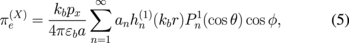
and  have to satisfy the scalar Helmholtz equation. In our derivations, the expressions for the Debye potentials of a radiating dipole in the absence of the metal NP are first determined. In the presence of the metal NP, we write the general expressions of the Debye potentials for the scattered fields due to the metal NP and apply the boundary conditions at r = R to obtain the following expressions. For a z-oriented dipole
  ,
,

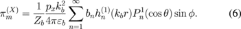
For an x-oriented dipole  ,
,
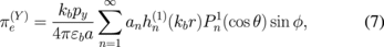
For a y-oriented dipole  ,
,
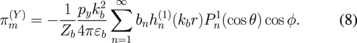
Here, ϕ is the azimuth angle,  ,
,


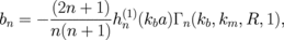
The corresponding scattered electromagnetic fields can then be calculated through


Here, the superscript S stands for (X), (Y), and (Z) in the cases of x-, y-, and z-oriented dipoles, respectively.
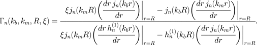
All the formulations above for a single dipole are used for evaluating the coupling behaviors of the whole system, including two dipoles and an Ag NP, through the interaction Hamiltonian,
where  is the dipole operator of dipole l and
  is the electric field at the position of dipole l. Each dipole is governed by its optical Bloch equations. Substituting all the analytically evaluated electric fields into the interaction Hamiltonian, and solving for the steady state solutions for each dipole, we can obtain the resultant dipole moments:
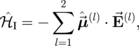
Here,  is the dipole matrix element for dipole l between states
  and
and  , T1 represents the spontaneous decay time, T2 = 2T1 stands for the dephasing time,46)
  denotes the population inversion of dipole l at zero field,
  is the projection amplitude of
  along
along  . Since
  is a function of both
  and
and  , Eq. (11) forms a set of strongly coupled nonlinear equations. They need to be solved with an iteration procedure.
Figure 3 shows the geometry of the dipole–LSP coupling system for numerical calculations. The location of dipole  is fixed at
  . Dipole
  is located at
  . In other words,
  and
and  lie on the same circle of a in radius centered at the Ag NP, separated by a polar angle θ in the x–z plane. To simplify the discussions, the two un-coupled dipoles,
  and
and  , are assumed to be oriented in the z-direction. The Ag NP and the two dipoles are embedded in a medium of εb = 6.25 for simulating the coupling behavior in GaN. In our numerical calculations, the NP radius, R, is fixed at 10 nm and the distance, a, is fixed at 50 nm.
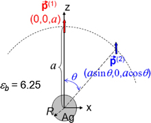
Fig. 3. Spatial distribution of the two radiating dipoles and the Ag NP to form the coupling system.
Download figure:
Standard image High-resolution image3.3. Numerical results
Figures 4(a) and 4(b) show the wavelength-dependent magnitude enhancement ratios of dipole moments when θ is fixed at 60° under the conditions with and without the Ag NP (labeled by "w NP" and "w/o NP", respectively). The dipole strength of the two in-phase un-coupled dipoles is assumed to be the same at  C·m. Because the coupling between the two z-oriented dipoles, either with or without the Ag NP, can result in the generation of the x-components, the enhancement ratios of the dipole moment magnitudes of both z- and x-components are shown in Figs. 4(a) and 4(b). Here, the enhancement ratio is defined as the coupled dipole moment magnitude normalized by the un-coupled value, p0. Figure 4(c) shows the wavelength dependence of the relative phase of the two coupled dipoles. In Figs. 4(a) and 4(b), the monotonically decreasing dashed curves show the coupling behavior of the two dipoles when the Ag NP does not exist. In this situation, the symmetric coupling leads to the same enhancement ratios for the two dipoles in either x- or z-component and in the total magnitude. Also, the relative phase of the two coupled dipoles is kept zero in either polarization when the Ag NP does not exist, as shown in Fig. 4(c). By including the LSP coupling through the Ag NP, Fano oscillation behaviors around 600 nm in the magnitude enhancement of dipole moment can be seen. In Fig. 4(a), the dipole moment magnitude and its z-component of either dipole are enhanced in the whole concerned spectral range. In a certain long-wavelength range (>580 nm for
  and >605 nm for
  ), the dipole moment magnitude with LSP coupling is larger than that without LSP coupling. The strengths of the generated x-components of the coupled dipoles (with LSP coupling) can reach 17% the original dipole strength. With LSP coupling, the relative phase of the two coupled dipoles can be as large as ∼−30° in the x-component.
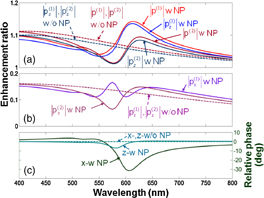
Fig. 4. (a), (b) Wavelength-dependent magnitude enhancement ratios of the dipole moments (the z-, x-component, and the total) when θ is set at 60° under the conditions with and without the Ag NP (labeled by "w NP" and "w/o NP", respectively). (c) Wavelength dependence of the relative phase of the two coupled dipoles. The strengths and phases of the two un-coupled dipoles are assumed to be individually the same.
Download figure:
Standard image High-resolution imageFigure 5 shows the wavelength-dependent enhancement ratios of the total radiated power and the scattered power of the coupling system. The scattered power is defined as that scattered by the Ag NP. It differs from the total radiated power by the direct radiations from the two dipoles, the interference related power, and the Ag NP absorption. The enhancement ratio here is defined as the totally radiated or scattered power normalized by the radiated power summation of the two un-coupled dipoles. The wavelength-dependent enhancement ratio of the scattered power indicates the LSP resonance around 590 nm. The Fano oscillation behavior around this wavelength can be seen in the enhancement ratio of the total radiated power when the LSP coupling is included. Without LSP coupling, the interaction between the two dipoles can also lead to the enhancement of total radiated power (almost double). With LSP coupling, the total radiated power can be enhanced by up to 150% around 623 nm in wavelength.

Fig. 5. Wavelength-dependent enhancement ratios of the total radiated power of the coupling system and the scattered power by the Ag NP when θ is 60° under the conditions with and without the Ag NP. The strengths and phases of the two un-coupled dipoles are assumed to be individually the same.
Download figure:
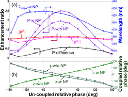
Standard image High-resolution imageFigure 6(a) shows the results of the enhancement ratios of the total radiated power (curves labeled by "P-w NP" and "P-w/o NP") and the dipole moment magnitudes in the cases with and without the Ag NP at the individual wavelengths of the maximum total radiated powers under the condition of LSP coupling when the polar angle between the two dipoles, θ, is varied from 10° through 180°. Here, the dipole moment magnitudes and phases of the two un-coupled dipoles are assumed to be individually the same. At each θ value, the wavelength for the maximum total radiated power is also plotted as the curve labeled by λmax-w NP. Also, the enhancement ratio difference of the total radiated power between the cases with and without the Ag NP as a function of θ is also demonstrated in the curve labeled by P-difference in Fig. 6(a). With LSP coupling, the wavelength for the maximum total radiated power is found to be in the range between 610 and 630 nm, i.e., around the LSP resonance wavelength. The enhancement ratio of the maximum total radiated power has a minimum value of ∼2.3 at θ = 90° and a maximum value of ∼3.1 at θ = 180°. The corresponding enhancement ratios in the case without LSP coupling are ∼2.0 at θ = 90° and ∼2.7 at θ = 180°. The large radiated power enhancements in the case without LSP coupling when θ is close to 180° is attributed to the large separation (100 nm) between the two dipoles for producing more constructive interference between the two radiation contributions. With LSP coupling, the total radiated power can be further enhanced by 31–68%, when compared with the coupling condition without the metal NP. The relative phases of the x- and z-components of the coupled dipoles as functions of θ are shown in Fig. 6(b). Again, the relative phase shifts only when the LSP coupling is included. Because the x-component under the condition of LSP coupling is quite weak when θ is larger than 150°, it becomes insignificant to determine the relative phase.

Fig. 6. (a) Enhancement ratios of the total radiated power (labeled by "P-w NP" and "P-w/o NP") and both dipole moment magnitudes in the cases with and without the Ag NP at the individual wavelengths of the maximum total radiated powers under the condition of LSP coupling when the polar angle between the two dipoles, θ, is varied from 10 to 180°. The wavelength for the maximum total radiated power is also plotted as the curve labeled by λmax-w NP. The enhancement ratio difference of the total radiated power between the cases with and without the Ag NP as a function of θ is plotted as the curve labeled by P-difference. (b) Relative phases of both x- and z-component of the coupled dipoles as functions of θ corresponding to the results in part (a). The strengths and phases of the two un-coupled dipoles are assumed to be individually the same.
Download figure:
Standard image High-resolution imageFigures 7(a) and 7(b) show the results similar to those in Figs. 6(a) and 6(b), respectively, except that θ is fixed at 60° and the relative phase of the two un-coupled dipoles of equal strength is varied. When the magnitude of the un-coupled relative phase is roughly larger than 120°, the total radiated power is suppressed under the condition with LSP coupling. The maximum enhancement is observed at 0° in un-coupled relative phase by about 150%, which is 54% more than the corresponding level in the case without LSP coupling. The relative phases of the two coupled dipoles in the cases with and without LSP coupling as functions of un-coupled relative phase are shown in Fig. 7(b). Without LSP coupling, the coupled relative phases of the x- and z-component (the dashed curve of "z-w/o NP" almost completely coinciding with the continuous curve of "z-w NP") are roughly mutually anti-symmetric with respect to the zero level. With LSP coupling, the coupled relative phases deviate slightly from the counterparts without LSP coupling. The deviation is larger in the x-component.
Fig. 7. Results similar to those in Fig. 6 except that θ is fixed at 60° and the relative phase of the two un-coupled dipoles is varied from −180° through 180°. The strengths of the two un-coupled dipoles are assumed to be the same.
Download figure:
Standard image High-resolution image
3.4. Discussion
In the case without the Ag NP, because the orientation of one dipole is different from the induced field direction of the other dipole, their interaction leads to the rotations of dipole orientations besides the changes of their strengths. Therefore, the x-polarization component of either dipole is generated. In this situation, the total radiated power of the two-dipole system is enhanced. By including the LSP coupling effect in the system of two dipoles plus the Ag NP, the dipole strengths, phases, and orientations are also affected by the electrical field oscillation strength, phase, and direction of the induced LSP resonance. In this situation, a more significant phase change is produced in either z- and x-polarization component. The LSP coupling process leads to a Fano oscillation in the spectral behavior of either dipole moment magnitude or total radiated power. On the long-wavelength side of the Fano oscillation, either dipole strength or total radiated power is further enhanced beyond the level of the case without the Ag NP. However, on the short-wavelength side, the dipole strength and total radiated power are reduced. In a light-emitting material with embedded metal NPs, the overall emission behavior can be regarded as the superposition of many LSP–dipole coupling systems, i.e., the superposition of many Fano oscillation patterns shown in Figs. 4 and 5. The superposition leads to the average effect of the Fano oscillations. Therefore, the wavelength-dependent enhancement ratio becomes smooth and can be lower than the maximum levels shown in Figs. 4 and 5.
As shown in Fig. 7, the variation of the enhancement ratio of total radiated power is quite sensitive to the un-coupled relative phase of the two dipoles. When the relative phase of the two un-coupled dipoles is small than a certain value (∼120°), enhanced total radiated power can be observed. Outside this relative phase range, the total radiated power is reduced. In a light-emitting material with embedded metal NPs, the LSP resonance of a metal NP may couple with many radiating dipoles. In this situation, the random phase distribution among those dipoles may average out the total radiated power to give an enhancement of a relatively lower level. Nevertheless, because the LSP coupling effect also depends on the relative positions of the dipoles, the combination of different positions and different phases among the dipoles coupled to the LSP mode of the same metal NP can result in a more complicated averaging effect. Although more dipoles can be considered in the theoretical and numerical studies based on the above formulations, the derivations and computations will become more complicated. Although it is difficult to evaluate the radiated power enhancement in a practical light-emitting material based on the above model, the study reported in this section can help us in understanding the fundamental mechanism of such an LSP–dipole coupling system for the development of light-emitting device.
3.5. Summary
In summary, by adopting a semi-classical model, including two two-level systems for the two radiating dipoles, an analytical expression for the electromagnetic field distribution, and an iterating procedure for obtaining the steady-state solution of the optical Bloch equations, we have built the theoretical formulations and numerical algorithms for evaluating the radiated power enhancement in the coupling process between two radiating dipoles and the LSP induced on a nearby Ag NP. Three mechanisms were considered in the coupling process for radiated power enhancement, including the interference of the two phase-retarded radiation contributions from the two dipoles, the interaction between the two dipoles, and the LSP resonant coupling. With the two dipoles located on a circle centered at the location of the Ag NP, with (without) LSP coupling, the total radiated power could be enhanced by 210 (170)%, depending on the un-coupled relative phase and the relative position of the two dipoles. Also, the relative phase of the two coupled dipoles was significantly changed.
4. Conclusions
In the first part of this paper, we have first reviewed the experimental implementations and theoretical/numerical investigations of SP coupled InGaN/GaN QW LEDs. SPP could be induced for coupling with a QW in a metal structure of a flat metal/GaN interface or a grating interface. An SPP mode on a flat interface could couple with a nearby radiating dipole for emission enhancement. However, a metal grating structure with a small enough grating period for momentum compensation could lead to a significantly stronger SP coupling effect. LSP modes could also be induced in a unit cell of a grating structure for effective SP coupling. If the p-GaN layer in an LED could be thin, surface metal NP represented an inexpensive structure for inducing SP coupling. When the p-GaN layer was thick, a few metal structures, including metal protrusion, buried metal NP, and embedded metal NP, could be used for effective SP coupling. In the numerical study, an algorithm, including the feedback effect of the induced SP resonance on the radiation behavior of the source dipole, has been proposed for studying the SP coupling effects with an embedded metal NP, a surface metal NP, and a metal protrusion. In the second part of this paper, we have built the theoretical formulations and numerical algorithms for evaluating the radiated power enhancement in the coupling process between two radiating dipoles and the LSP induced on a nearby Ag NP. Three mechanisms were considered in the coupling process for radiated power enhancement, including the interference of the two phase-retarded radiation contributions from the two dipoles, the interaction between the two dipoles, and the LSP resonant coupling.
Acknowledgments
This research was supported by Ministry of Science and Technology, Taiwan, The Republic of China, under the grants of NSC 102-2221-E-002-204-MY3, NSC 102-2120-M-002-006, and NSC 101-2622-E-002-002-CC2, NSC 102-2221-E-002-199, by the Excellent Research Projects of National Taiwan University (102R890951 and 102R890952), and by US Air Force Scientific Research Office under the contract of AOARD-13-4143.