Abstract
Currently, organic light-emitting diodes (OLEDs) have reached the stage of commercialization, and there are intense efforts to use them in various applications from small- and medium-sized mobile devices to illumination equipment and large TV screens. In particular, phosphorescent materials have become core OLED materials as alternatives to the conventionally used fluorescent materials because devices made with phosphorescent materials exhibit excellent light-emitting performance. However, phosphorescent materials have several problems, such as their structure being limited to organic metal compounds containing rare metals, for example, Ir, Pt, and Os, and difficulty in realizing stable blue light emission, so the development of new materials is necessary. In this article, I will review next-generation OLEDs using a new light-emitting mechanism called thermally activated delayed fluorescence (TADF). Highly efficient TADF, which was difficult to realize with conventional technologies, has been achieved by optimizing molecular structures. This has led to the realization of ultimate next-generation OLEDs that are made of common organic compounds and can convert electricity to light at an internal quantum efficiency of nearly 100%.
Export citation and abstract BibTeX RIS
1. Introduction
Materials are classified into three groups in terms of electrical conductivity: insulators, semiconductors, and metals. In general, organic compounds composed of carbon skeletons act as insulators, as exemplified by plastic materials. However, a rather different property is obtained by forming an ultrathin film of such insulating organic compounds with a thickness of approximately 0.1 µm. When electrodes are attached to both sides of the organic thin film and a voltage of approximately 10 V is applied, electrons and holes can overcome the energy barriers and are injected from the anode and cathode, respectively, into the film. These injected carriers move toward the opposite electrode following the electric potential gradient. When the electrons and holes recombine at a molecule, a high-energy state (exciton) is induced. Photons are emitted when the excited state returns to the ground state. This is called organic electroluminescence (EL). Because of the ultrathin film structure, a high electric field of 106 V/cm can be generated in the organic thin film. Under such an extreme condition, carriers are injected from the electrodes to the organic thin film and become capable of easily moving between molecules. Thus, unprecedented functions can be expressed in this extreme state.
In 1950, Japanese scientists including Inokuchi and Akamatsu, who proposed the application of electrical current to organic compounds, discovered organic semiconductors.1) In 1965, EL from an organic compound was observed for the first time from an anthracene single crystal by Helfrich and Schneider2) (Fig. 1). Helfrich and colleagues also carried out research on liquid crystals in those days, which was the dawn of liquid crystals. It is interesting that they also invented twisted nematic (TN) liquid crystals. At that time, engineers discussed whether organic light-emitting diodes (OLEDs) or liquid crystals were more suitable for display devices, as can be seen in the literature of those days. Eventually, liquid crystals were focused on as a research target for display devices, and the target of research on OLEDs shifted from single crystals to ultrathin films for realizing low-voltage operation. Now, OLEDs have reached the stage of commercialization through their research over the past five decades, albeit two decades behind the commercialization of liquid crystals. In particular, the research and development of OLEDs has rapidly accelerated since 1990, and their practical application has leaned toward small display devices, such as mobile phones and MP3 players, and flat panel TV screens since 2000. If π-electron orbitals of adjacent molecules sufficiently overlap, electric charges can move between the molecules in a strong electric field; consequently, thin films of organic compounds can be used as semiconductor thin films. Such a method has been established by developing OLEDs and has led to the emergence of novel semiconductors, that is, organic semiconductors.

Fig. 1. History of research and development of organic semiconductors. The concept of organic semiconductors was established in the 1950s and 1960s. The research fields of conductive polymers and OPCs were established in the 1970s and 1980s. The full-scale research and development of organic electronic devices actively using a current density on the order of mA/cm2 started from the 1980s. Afterwards, the research and development of OLEDs, OSCs, organic transistors, and organic memories was carried out extensively, from basic research to practical application. Organic semiconductors are expected to be applied to bioelectronics in the future.
Download figure:
Standard image High-resolution imageOrganic photoconductors (OPCs) were the first commercialized electronic devices using organic semiconductors and are the heart of copiers and laser printers used daily in offices. When the charged layer formed on the surface of an OPC is irradiated with light, current flows through the organic semiconductor layer to form a latent image. OPCs have now become a main field of industry as a result of the dramatic spread of laser printers and copiers. The materials currently used in OLEDs are an extension of the materials developed for OPCs. Since the early 1990s, various molecular skeletons were designed and synthesized on the basis of the molecular design for OPCs. Fluorescent materials and devices were mainly developed in the 1990s, and phosphorescent materials and devices have been in development since around 2000. Electron transport materials are a key point in the development of OLED materials, and the molecular design for organic materials that conduct electrons has been established through the research on OLEDs.3) Based on OLED research achievements, a wide range of research and development of next-generation organic devices, such as organic solar cells (OSCs), organic transistors, organic memories, and organic semiconductor lasers, is now ongoing.
In the history of research on the above-mentioned organic optoelectronics, OLEDs were the first devices based on organic thin films capable of being operated at current densities as low as the mA/cm2 order and are considered to be the core organic optoelectronic devices realized by utilizing organic compounds as semiconductors. Since 2000, organic electronics has become not only an independent academic field but also a new established industry, and is beginning to gain market value. The new organic semiconductor materials, device physics, and device engineering developed in relation to OLEDs have been applied to the creation of new next-generation devices. Thus, a new industrial field of electronics has evolved.
2. Application of OLEDs to next-generation organic devices
OLEDs have many excellent basic characteristics, such as self-luminescence, surface luminescence, high flexibility, high resolution, and high EL efficiency. Through research and development over the past 25 years, device characteristics superior to those of liquid crystals have been obtained. However, OLEDs still have several problems to be solved to improve their performance: high cost due to the use of noble metals such as Ir and Pt as emitting materials, difficulty in achieving stable blue light emission, and low device stability and yield because of the use of organic ultrathin films with a thickness of approximately 100 nm. Thus, the potential excellent device characteristics of organic semiconductors have not yet been fully obtained. In addition, improving the efficiency of extracting light from thin films by introducing photonic crystals and light scattering techniques has been widely discussed; however, no decisive solutions have been obtained.4) Moreover, the high definition required for medium- and small-sized OLED displays is the greatest challenge. To realize this, RGB coloring at a 10 µm order of accuracy is required, and an innovative process must be developed to realize low-cost mass production. Currently, the following four points are necessary to realize next-generation OLEDs: (1) realization of highly efficient luminescence without using phosphorescent materials, (2) utilization of the intrinsic optical and electronic anisotropies of molecules, (3) development of an RGB coloring process for achieving high definition, and (4) creation of a low-cost fabrication process.
Recently, research on thin-film OSCs has become popular. Similar to OLEDs, OSCs have a long history of research and have been experimentally examined since the 1970s. In recent years, comprehensive research on OSCs has been carried out jointly by scientists in industry and in academia, and a power conversion efficiency exceeding 10% has been reported.5) The materials and processes for OSCs are expected to be developed aiming for their industrialization in the future. Moreover, an increasing number of research groups are focusing on (1) the realization of multifunctional single materials on the basis of the diversity of design for organic materials and (2) the pursuit of achieving ultimate performance in optoelectronic devices. The former includes research on organic spintronics using organic magnetic materials6) as a new target of research. The latter includes research on organic semiconductor lasers7) and organic memories,8) and in particular, organic semiconductor lasers are attracting attention for tackling the challenge of attaining the ultimate performance of organic electronics.
3. Latest trend of OLEDs
At present, OLEDs are expected to be practically applied to flat panel displays and illumination sources because they have unique characteristics, such as high EL efficiency and flexibility, and can be processed at low temperatures. Thus far, various fluorescent and phosphorescent materials have been developed to improve the EL efficiency of OLEDs.9–11) As a result, highly durable and practically applicable OLEDs using fluorescent materials have been realized. However, the internal quantum efficiency (ηint), which is defined as the ratio of the number of photons that can be extracted for EL to the injected current (i.e., the number of injected carriers), was only 25% because of the limit imposed by the statistics of the electron spin state under electrical excitation.12,13) In contrast, OLEDs using phosphorescent materials based on luminescence from the triplet state can achieve ηint = 100%.14) However, the design of molecules used in such OLEDs is greatly limited because the heavy atom effect (spin–orbital interaction) must be induced, for example, by using rare metals, to realize highly efficient radiative transition from the triplet excited state to the ground state.
Previously, researchers reported several methods of achieving an ηint higher than the theoretical limit (25%) for OLEDs without using Ir complexes. Specifically, a method of developing phosphorescent materials that are free of rare metals15,16) and a method of generating a singlet excited state by triplet–triplet annihilation (TTA)17) have been reported. For OLEDs using phosphorescent materials, TTA leads to the deactivation of triplet excitons and hence decreases the EL quantum efficiency; however, for OLEDs using fluorescent materials, the concentration of singlet excitons can be increased by TTA. Delayed fluorescence attributed to TTA was already confirmed from the EL phenomenon observed in an anthracene single crystal in the 1960s, indicating that triplet excitons actively move around and interact in an organic solid thin film. Hence, scientists have examined the application of the generation of single excitons attributed to TTA for improving the EL efficiency.17) In actuality, the external quantum efficiency ηext has been reported to exceed its theoretical limit (5%) in some OLEDs using fluorescent materials, demonstrating the applicability of TTA as seen in the transient EL characteristics. However, the efficiency of generating singlet excitons by TTA is only 37.5% at maximum, and a novel luminescence mechanism is required.
Recently, our research group has proposed a method of achieving an ηint of 100% through up-conversion from the triplet excited state, which is generated at a probability of 75% upon electrical excitation, to the singlet excited state.18) This method can be used to cause the triplet excited state to contribute to luminescence without using rare metals. The method involves the up-conversion of triplet excitons to singlet excitons using thermal energy and has long been known as E-type delayed fluorescence in the field of photochemistry. Well-known materials that exhibit thermally activated delayed fluorescence (TADF) are eosin,19) fullerene,20) and porphyrin21) derivatives. Although the TADF process was considered to show a low power-conversion efficiency because it is generally an endothermic reaction, recent studies have revealed that highly efficient delayed fluorescence can be achieved by optimizing the molecular design.
TADF characteristics depend on the probability of reverse intersystem crossing (RISC) from the triplet to singlet excited states. The EL efficiency increases as the energy difference between the singlet and triplet excited states (ΔEST) decreases. For example, condensed polycyclic aromatic compounds, such as anthracene, exhibit very intense fluorescence but are not expected to show efficient TADF because their ΔEST exceeds 1 eV. In contrast, ketone-based materials, such as benzophenone derivatives, have a relatively small ΔEST (= 0.1–0.2 eV) but do not exhibit intense luminescence at room temperature and only exhibit phosphorescence at low temperatures.22)
Here, the dominant factor of ΔEST is examined from the viewpoint of quantum chemistry. ΔEST is proportional to the exchange integral and decreases as the overlap between the wave functions of the ground and excited states decreases. When the nonbonding n-electron orbital and the excited π-electron orbital (n–π* orbital) of, for example, benzophenone overlap orthogonally, ΔEST becomes small because of its small overlap integral. In contrast, aromatic compounds with a π-electron system generally have a large overlap of the π–π* orbital, resulting in a large ΔEST of over 1 eV. Here, a relatively large radiative rate constant (kr) is required to obtain a high EL efficiency. In the case of the above-mentioned aromatic compounds, however, a large overlap between the wave functions of the ground and excited states is required. Therefore, it is necessary to design molecules that exhibit highly efficient EL while maintaining a small ΔEST. Because large kr and small ΔEST are conflicting, fine molecular design is required to realize them simultaneously. We carefully designed and created a novel molecule that has a small ΔEST and can exhibit highly efficient EL (Fig. 2). Specifically, we designed and synthesized novel compounds that contain both electron-donating and electron-accepting substituents and successfully created a luminescent molecule showing an EL efficiency of nearly 100% while maintaining a very small ΔEST (< 0.2 eV). This molecule allows the up-conversion from the triplet excited state generated upon electrical excitation to the singlet excited state, enabling the realization of highly efficient EL equivalent to that of phosphorescent devices from the singlet excited state. In particular, an ultimate level of external efficiency close to 20% was achieved in the green range (wavelength, 530 nm) for an OLED employing carbazolyl dicyanobenzene (CDCB) as an emitting layer.23) In addition, we found that an intrinsically small ΔEST can be achieved in exciplexes, which are intermolecular complexes, and successfully obtained an ηext higher than 10% by selecting the optimal materials.

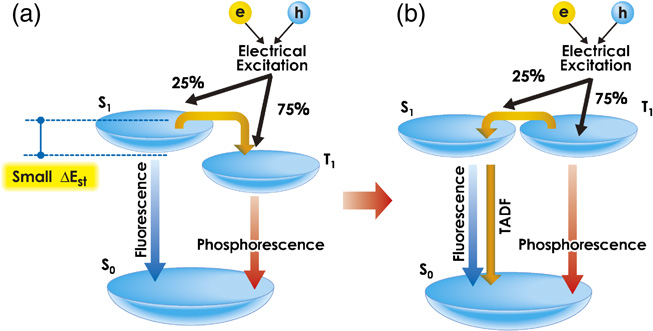
Fig. 2. Generation process of singlet and triplet excitons upon electrical excitation. (a) Conventional fluorescent and phosphorescent materials. (b) For TADF materials, the S1 and T1 levels are close to each other and reverse energy transfer occurs with a high efficiency, enabling highly efficient EL from the S1 level.
Download figure:
Standard image High-resolution imageIn the following sections, I will introduce a method of up-conversion based on intramolecular charge transfer (ICT) that achieves a high ηint that exceeds its theoretical limit of 25% for traditional fluorescent OLEDs, new organic light-emitting materials suitable for this approach, and the organic EL characteristics of devices employing these new materials. I will also introduce an exciplex system, which is the excited state formed between donor and acceptor molecules, as an alternative method to improving ηint through up-conversion.
4. TADF characteristics of triazine derivatives
In the development of high-efficiency TADF materials, it is necessary to design molecules with excellent EL characteristics while maintaining a small ΔEST. Namely, the key is the design of molecules that can simultaneously achieve both large kr and small ΔEST. Here, the design of molecules that achieve small ΔEST is examined. In general, the highest occupied molecular orbital (HOMO) is distributed in the electron-donating units, whereas the lowest unoccupied molecular orbital (LUMO) is distributed in the electron-accepting units. Therefore, a small ΔEST can be obtained by introducing electron-donating and electron-accepting groups inside the molecules to decrease the spatial overlap between the HOMO and LUMO. On the basis of this direction of molecular design, we designed and synthesized a novel molecule, 2,4-bis{3-(9H-carbazol-9-yl)-9H-carbazol-9-yl}-6-phenyl-1,3,5-triazine (CC2TA), in which the acceptor phenyltriazine unit is used as the central skeleton and donor bicarbazole units are bonded to both ends of the skeleton (Fig. 3).24) Molecular orbital calculations reveal that the HOMO and LUMO are locally distributed mainly in the bicarbazole and phenyltriazine units, respectively. As a result, the molecule successfully showed a very small ΔEST of 0.06 eV. In CC2TA, the introduction of bicarbazole with a Wurster structure (>N–aryl–N<) as a donor was the key to obtaining a small ΔEST. If a simple carbazole was bonded as a donor, the HOMO and LUMO would overlap to some extent, resulting in an increased ΔEST of 0.35 eV.

Fig. 3. Molecular structure and orbitals of a TADF material with a triazine skeleton (CC2TA).
Download figure:
Standard image High-resolution imageTo evaluate the TADF characteristics of CC2TA, the PL characteristics of a co-evaporated thin film, obtained by dispersing 6 wt % CC2TA into a bis[2-(diphenylphosphino)phenyl]ether oxide (DPEPO) host, are shown in Fig. 4. The triplet energy (ET) of the DPEPO host is 3.1 eV, so triplets in CC2TA (ET = 2.85 eV) can contribute to efficient luminescence without being transferred to the host. Figure 4(a) shows time-resolved PL spectra (streak images) of the CC2TA:DPEPO co-evaporated thin film. At room temperature, both prompt (lifetime, τ = 27 ns) and delayed (τ = 22 µs) PL components are observed in the same wavelength range. Figure 4(b) shows the temperature dependence of the transient PL waveform. The intensity of the delayed PL component markedly increases with increasing temperature. This result suggests that RISC from triplet to singlet excited states actively occurs in the temperature range around room temperature owing to thermal energy, resulting in efficient TADF. In contrast, the triplet excitons cannot overcome the energy barrier to the singlet excited state at a low temperature (150 K). Therefore, RISC scarcely occurs and intense delayed fluorescence is not observed.

Download figure:
Standard image High-resolution image
Fig. 4. (a) Time-resolved PL spectra of 6 wt % CC2TA:DPEPO co-evaporated thin film and (b) temperature dependence of the transient PL waveform.
Download figure:
Standard image High-resolution imageNext, the characteristics of an OLED employing the CC2TA:DPEPO co-evaporated thin film as an emitting layer are shown (Fig. 5). The maximum external quantum efficiency reaches ΦEL(ext) = 11%. Here, the efficiency of EL involving TADF can be expressed by

Here, ηr,S and ηr,T are the probabilities of generation of the singlet and triplet excitons (ηr,S = 25%, ηr,T = 75%), ΦF is the fluorescence quantum yield (ΦF = 16%), ΦTADF is the TADF quantum yield (ΦTADF = 46%), and ΦISC is the probability of intersystem crossing (ΦISC = 84%). From Eq. (1), the theoretical internal quantum efficiency (ηint) is calculated to be 56%. Assuming the light-extracting efficiency to be 20%, the theoretical external quantum efficiency (ηext) is 11%, which is in good agreement with the value obtained in our experimental device.

Download figure:
Standard image High-resolution image
Fig. 5. (a) Device structure and relationship between current density and voltage and (b) dependence of external quantum efficiency (ηext) on current density for TADF-OLED employing CC2TA as an emitting layer.
Download figure:
Standard image High-resolution image5. TADF characteristics of spiro derivatives
5.1. Development of TADF materials with spirobifluorene skeletons
Spiro compounds are expected to exhibit TADF because donor and acceptor units can be introduced into their orthogonal π-conjugated system and the HOMO and LUMO can be spatially separated.25) Figure 6 shows the molecular structure of a spirobifluorene derivative (Spiro-CN) that exhibits TADF. This molecule has two donor triarylamino groups and two acceptor cyano groups. The molecules between these groups are distorted by the spirobifluorene skeleton to form a twisted steric structure. As shown in the result of molecular orbital calculations in Fig. 6, the HOMO and LUMO are locally distributed in the triarylamino-based fluorene and cyano-based fluorene, respectively.

Download figure:
Standard image High-resolution image
Download figure:
Standard image High-resolution image
Fig. 6. (a) Molecular structure, (b) HOMO, and (c) LUMO of Spiro-CN. Reproduced from Ref. 25 by permission of The Royal Society of Chemistry.
Download figure:
Standard image High-resolution imageFigure 7(a) shows the PL spectrum of a Spiro-CN:m-CP co-evaporated thin film, in which 6 wt % Spiro-CN guest is dispersed in an m-CP host. The transient waveform consists of a prompt PL component with τ ≈ 24 ns and a delayed PL component with τ ≈ 14 µs. Figure 7(b) shows the temperature dependence of PL characteristics for the 6 wt % Spiro-CN:m-CP co-evaporated thin film. The prompt fluorescence component shows no temperature dependence, whereas the PL intensity of the delayed fluorescence component clearly increases with temperature. This indicates that RISC from triplet to singlet excited states actively occurs with increasing temperature. The results of evaluating ΔEST using the Berberan–Santos equation on the basis of the above-mentioned temperature dependence of PL characteristics are shown below. Here, it is assumed that Φprompt is the prompt fluorescence quantum yield, Φdelayed is the delayed fluorescence quantum yield, ΦT is the efficiency of generating triplet exitons, kp is the radiative rate constant from the triplet excited state, knr is the nonradiative rate constant from the triplet excited state, kRISC is the rate constant for RISC, and R is the gas constant. Then, the Berberan–Santos equation is given by

Figure 7(c) shows the Berberan–Santos plots of PL characteristics of the 6 wt % Spiro-CN:m-CP co-evaporated thin film. ΔEST of Spiro-CN is estimated to be 0.057 eV from the slope of the straight line in the figure. This demonstrates that ΔEST of Spiro-CN is much smaller than that of conventional delayed fluorescent materials, such as C70 (0.26 eV) and tin(IV)fluoride-porphyrin (0.24 eV).

Download figure:
Standard image High-resolution image
Download figure:
Standard image High-resolution image
Fig. 7. (a) Transient PL spectrum of 6 wt % Spiro-CN:m-CP co-evaporated thin film. The inset shows time-resolved PL spectra (red line, PL spectrum attributed to prompt fluorescence component; black line, PL spectrum attributed to delayed fluorescence component). (b) Temperature dependence of PL quantum yield (○, total; △, delayed fluorescence component; □, prompt fluorescence component). (c) Berberan–Santos plots of temperature dependence of PL intensity. Reproduced from Ref. 25 by permission of The Royal Society of Chemistry.
Download figure:
Standard image High-resolution imageNext, the EL characteristics of an OLED employing the 6 wt % Spiro-CN:m-CP co-evaporated thin film as an emitting layer were measured. A maximum ηext of 4.4% was obtained for an OLED with a structure of indium tin oxide (ITO)/α-N,N'-di(1-naphthyl)-N,N'-diphenylbenzidine (NPD)/6 wt % Spiro-CN:m-CP/Bphen/MgAg/Ag. This value greatly exceeds the theoretical value of ηext when a conventional fluorescent material with a fluorescence quantum yield of 27% is used as an emitting layer (i.e., ηext = 1.4%), meaning that the efficiency of generating excitons is increased by TADF.
5.2. Development of TADF materials with spiro-acridine skeletons
As mentioned above, spiro compounds have been found to have great potential for use as TADF materials. The TADF characteristics of a new spiro compound with an acridine unit as a donor moiety (ACRFLCN) have been reported.26) Figure 8(a) shows a transient PL spectrum of a 6 wt % ACRFLCN:TRSi-F co-evaporated film. In the transient PL spectrum, a delayed fluorescence component with a lifetime of 4.5 ms is observed in addition to a prompt fluorescence component with a nanosecond-order lifetime. The luminescence attributed to the long-lifetime component is delayed fluorescence because the PL spectrum from the long-lifetime component is in agreement with the fluorescence spectrum from the short-lifetime component. As shown in Fig. 8(b), the PL quantum yield of the 6 wt % ACRFLCN:TRSi-F co-evaporated film is 9.7% in the presence of oxygen, whereas it greatly increases to 67.3% in a nitrogen-rich environment. This result indicates that the delayed fluorescence component is quenched owing to the presence of oxygen.

Download figure:
Standard image High-resolution image
Fig. 8. (a) Transient PL spectrum of 6 wt % ACRFLCN:TPSi-F co-evaporated film. (b) Oxygen dependence of PL quantum yield of 6 wt % ACRFLCN:TPSi-F co-evaporated film.
Download figure:
Standard image High-resolution imageAs mentioned above, highly efficient delayed fluorescence with a total PL quantum yield of 67% was observed for the ACRFLCN, where the donor units of the Spiro-CN are expanded from fluorene to acridine. In addition, a high ηext of 10% was confirmed at a low current density of 10−3 mA/cm2 for an OLED with a structure of ITO/4,4'-cyclohexylidenebis[N,N-bis(4-methylphenyl)benzenamine] (TAPC) (40 nm)/m-CP (5 nm)/6 wt % ACRFLCN:TPSi-F (20 nm)/TmPyPB (35 nm)/LiF (1 nm)/Al (60 nm), as shown in Fig. 9.26)

Fig. 9. Dependence of ηext on current density for OLED employing ACRFLCN as an emitting layer.
Download figure:
Standard image High-resolution image6. TADF characteristics of phenoxazine derivatives
As mentioned above, the HOMO and LUMO can be spatially separated by largely twisting the donor and acceptor units, and a small ΔEST can thereby be achieved. 10-(4-(4,6-diphenyl-1,3,5-triazin-2-yl)phenyl)-10H-phenoxazine (PXZ-TRZ), shown in Fig. 10, is a compound with a large torsion angle (74.9°) at the binding site of the donor and acceptor, and its calculated ΔEST is very small (0.01 eV).27) This nearly zero calculated ΔEST is due to the largely twisted molecular structure that allows the HOMO and LUMO to be almost completely separated. PXZ-TRZ shows delayed fluorescence with a peak at a position similar to that of fluorescence and can be used as a zero-gap TADF material with ΔEST ≈ 0, as expected by calculation.

Fig. 10. Molecular structure, HOMO, and LUMO of PXZ-TRZ. Reproduced from Ref. 25 by permission of The Royal Society of Chemistry.
Download figure:
Standard image High-resolution imageFigure 11 shows the result of evaluating the characteristics of an OLED employing PXZ-TRZ with a device structure of ITO/α-NPD (35 nm)/6 wt % PXZ-TRZ:4,4'-bis(N-carbazolyl)biphenyl (CBP) (15 nm)/2,2',2''-(1,3,5-benzinetriyl)-tris(1-phenyl-1-H-benzimidazole) (TPBi) (65 nm)/LiF (0.8 nm)/Al (80 nm). ηext is as high as 12.5%, and the roll-off characteristics at high current densities are small. The OLED exhibits green emission, and the Commission Internationale de l'Eclairage (CIE) chromaticity coordinates are  at a current density of 10 mA/cm2. The transient PL characteristics of the 6 wt % PXZ-TRZ:CBP co-evaporated film reveal that efficient up-conversion from T1 to S1 via RISC is realized in PXZ-TRZ. Thus, TADF materials showing a high external quantum efficiency can be created by twisting molecular skeletons to achieve a zero gap.

Fig. 11. ηext–J (current density) characteristics of OLED employing PXZ-TRZ as an emitting layer. The inset shows the EL spectrum. Reproduced from Ref. 25 by permission of The Royal Society of Chemistry.
Download figure:
Standard image High-resolution image7. TADF characteristics of CDCB derivatives
Although a small ΔEST can be achieved by spatially separating the HOMO and LUMO as mentioned above, this spatial separation generally decreases the transition dipole moment μ and hence decreases the EL quantum yield. To realize highly efficient TADF, a small ΔEST and a large μ must be simultaneously achieved while maintaining the appropriate level of overlap between the HOMO and LUMO.
Figures 12(a)–12(c) show the molecular structure, HOMO, and LUMO, respectively, of a CDCB derivative designed following the above-mentioned theory.23) The HOMO and LUMO are locally distributed in the donor carbazolyl groups and the acceptor dicyanobenzene units, respectively. It is apparent that the HOMO and LUMO moderately overlap on the central benzene ring. This indicates that the CDCB derivative achieves both small ΔEST and large μ. Quantum chemical calculations also reveal that the change in the molecular structure among the S0, S1, and T1 states is small in 4CzIPN. From this result, 4CzIPN is expected to achieve a high EL quantum yield as a result of the suppressed nonradiative deactivation process.

Download figure:
Standard image High-resolution image
Download figure:
Standard image High-resolution image
Fig. 12. (a) Molecular structure of CDCB derivatives and (b) HOMO, (c) LUMO, and (d) absorption and PL spectra of 4CzIPN.
Download figure:
Standard image High-resolution imageFigure 12(d) shows the absorption and PL spectra of 4CzIPN in toluene solution. 4CzIPN has a wide PL band of approximately 507 nm attributed to ICT. The stokes shift of 4CzIPN is smaller than that in conventional ICT-based luminescence. This means that the change in the molecular structure of 4CzIPN is small in electron excitation from the S0 to S1 states.
Next, the TADF characteristics of a 6 wt % 4CzIPN:CBP co-evaporated film will be discussed. Figure 13(a) shows the PL transient decay characteristics of this film at 100, 200, and 300 K. PL transient decay characteristics comprising two types of components, a nanosecond-order short-lifetime component and a microsecond-order long-lifetime component, are observed at any temperature. Figure 13(b) shows time-resolved PL spectra of the short- and long-lifetime components at 300 K. Luminescence attributed to the long-lifetime component is delayed fluorescence because the PL spectrum from the long-lifetime component is in agreement with the fluorescence spectrum from the short-lifetime component. Figure 13(c) shows the temperature dependences of the PL quantum yields of the prompt and delayed fluorescence components. The prompt fluorescence quantum yield slightly increases with decreasing temperature. This is due to the suppressed nonradiative deactivation process. In contrast, the delayed fluorescence quantum yield markedly decreases with decreasing temperature. This is due to the suppression of RISC from the T1 to S1 states with decreasing temperature.

Download figure:
Standard image High-resolution image
Fig. 13. (a) PL transient decay, (b) time-resolved PL spectra, (c) temperature dependence of PL quantum yield, and (d) Arrhenius plot of the rate constant of RISC for 6 wt % 4CzIPN:CBP co-evaporated film.
Download figure:
Standard image High-resolution imageThe ΔEST of 4CzIPN can be estimated from the temperature dependence of the PL quantum yield observed above. Here, the rate constant for RISC from the T1 to S1 states (kRISC) is expressed using the rate constant for prompt fluorescence (kp), the rate constant for delayed fluorescence (kd), the prompt fluorescence quantum yield (Φp), the delayed fluorescence quantum yield (Φd), and the rate constant for intersystem crossing (kISC) from the S1 to T1 states as follows:

Since kp and kd can be determined from the transient PL curve and Φp and Φd can be measured, kRISC can be evaluated using Eq. (3). kRISC and ΔEST have a relationship that can be expressed by kRISC ∼ A exp(−ΔEST/kBT), where A is a constant, kB is the Boltzmann constant, and T is the temperature. Therefore, ΔEST can be calculated from the temperature dependence of kRISC. Figure 13(d) shows the Arrhenius plots of kRISC between 200 and 300 K. ΔEST is calculated to be 83 meV from the slope of the straight line in the figure. This demonstrates that the energy difference between the S1 and T1 states is small for 4CzIPN.
Figure 14 shows the characteristics of OLEDs employing CDCB derivatives as an emitting layer with the structure of ITO/α-NPD (35 nm)/6 wt % CDCB:CBP (15 nm)/TPBi (65 nm)/LiF (0.8 nm)/Al (80 nm). The external quantum efficiencies of 4CzPN, 4CzIPN, and 4CzTPN are all very high, 17.8, 19.3, and 17.1%, respectively. This means that 4CzIPN, which shows a particularly high external quantum efficiency, has an internal quantum efficiency of nearly 100%.

Fig. 14. ηext–J (current density) characteristics of OLED employing CDCB derivative as an emitting layer. The inset shows the EL spectra.
Download figure:
Standard image High-resolution image8. TADF characteristics of exciplexes
In the radiation transition of organic compounds, electrons generally transit from the LUMO to the HOMO within a single molecule. In the excited state formed within a single molecule, therefore, the HOMO and LUMO are confined in the molecule, causing the electron exchange integral to be large. This results in an increased ΔEST. We focused on the exciplex state, which is the excited state formed between electron-donating and electron-accepting molecules. In the radiation process of exciplexes, charges transit from the LUMO of the electron-accepting molecule to the HOMO of the electron-donating molecule. Therefore, the electron exchange integral of the exciplex is small because the HOMO and LUMO are spatially separated, resulting in a very small ΔEST. This increases the probability of up-conversion from the triplet to singlet excited states.
Here, the up-conversion from the triplet to singlet excited states is explained using the exciplex formed between electron-donating 4,4',4''-tris[3-methylphenyl(phenyl)amino]triphenylamine (m-MTDATA) and electron-accepting 2-(biphenyl-4-yl)-5-(4-tert-butylphenyl)-1,3,4-oxadiazole (t-Bu-PBD).28) Figure 15(a) shows the PL spectrum of a 50 mol % m-MTDATA:t-Bu-PBD co-evaporated film as well as the fluorescence and phosphorescence spectra of m-MTDATA and t-Bu-PBD single thin films. The PL intensity peak for the co-evaporated film appears at a wavelength of 540 nm, which is longer than that of the peaks for fluorescence from the m-MTDATA and t-Bu-PBD thin films. This is because an exciplex is formed between the molecules of m-MTDATA and t-Bu-PBD.

Download figure:
Standard image High-resolution image
Fig. 15. (a) PL spectrum of 50 mol % m-MTDATA:t-Bu-PBD co-evaporated film and fluorescence and phosphorescence spectra of m-MTDATA and t-Bu-PBD single thin films. (b) Temperature dependence of kRISC.
Download figure:
Standard image High-resolution imageTo achieve a high up-conversion probability, attention should be paid to the confinement of the triplet excited state of the exciplex resulting from the triplet excited states of electron-donating and electron-accepting materials because energy can be transferred from the triplet excited state of the exciplex to the triplet excited states of electron-accepting and electron-donating materials to cause nonradiative deactivation at each triplet excited state, resulting in a markedly decreased up-conversion probability. The phosphorescence intensity peak for the m-MTDATA thin film appears at 475 nm, which means that the triplet excited state of the exciplex is sufficiently confined. On the other hand, the phosphorescence intensity peak for the t-Bu-PBD thin film appears at approximately 510 nm,29) again indicating that the triplet excited state of the exciplex is sufficiently confined by that of t-Bu-PBD and that a high up-conversion probability can be expected. In practice, delayed fluorescence resulting from the fluorescence component of the exciplex and the up-conversion from the triplet to singlet excited states has been confirmed in the transient PL characteristics of the 50 mol % m-MTDATA:t-Bu-PBD co-evaporated film at room temperature.
ΔEST of the exciplex formed between t-Bu-PBD and m-MTDATA was estimated by measuring the temperature dependence of the rate constant for RISC, kRISC, which is given by

Here, A is a constant, kB is the Boltzmann constant, and T is temperature. Using Eq. (4), ΔEST can be estimated from the temperature dependence of kRISC. kRISC can be estimated from the rate constants and the PL quantum yields of the prompt and delayed fluorescence components using Eq. (3).28) kp, kd, Φp, and Φd can be experimentally determined from the PL decay curve and the temperature dependence of the PL intensity. The Arrhenius plots of kRISC calculated using Eq. (3) are shown in Fig. 15(b). Here, kISC is assumed to be independent of temperature. The activation energy was 50 meV, demonstrating that the singlet and triplet excited states of the exciplex are very close.
Although ΔEST of the exciplex formed between m-MTDATA and t-Bu-PBD is found to be small, the EL efficiency of OLEDs with the m-MTDATA:t-Bu-PBD co-evaporated film as an emitting layer is still low (∼2%). We examined delayed fluorescence from the exciplex formed between various donor and acceptor materials. As a result, intense delayed fluorescence was observed in the exciplex formed between m-MTDATA as the donor material and 2,8-bis(diphenyl phosphoryl)dibenzo[b,d]thiophene (PPT) as the acceptor material.30) Figure 16(a) shows the PL spectrum of a 50 mol % m-MTDATA:PPT co-evaporated film as well as the fluorescence and phosphorescence spectra of m-MTDATA and PPT single thin films. The PL intensity peak of the co-evaporated film appears at a wavelength of 520 nm, which is longer than the fluorescence intensity peaks from the m-MTDATA and PPT single thin films, meaning that exciplexes are formed in the co-evaporated film. The PL quantum yield of the exciplex formed between m-MTDATA and PPT is 28.5% and is higher than that of the exciplex formed between m-MTDATA and t-Bu-PBD (19.6%). In addition, the PL quantum yield of the delayed fluorescence component is 25.4% and is higher than that for the exciplex formed between m-MTDATA and t-Bu-PBD (8.2%). To evaluate the effect of the increased PL quantum efficiency of delayed fluorescence, the characteristics of OLEDs with the structure of ITO/m-MTDATA (35 nm)/X mol % m-MTDATA: PPT (30 nm)/PPT (35 nm)/LiF/Al are shown in Fig. 16(b). ηext of the OLED is 10.0%, which exceeds the theoretical limit of 5% for devices using fluorescent materials. Thus, delayed fluorescence from the exciplex state as an intermolecular charge-transfer excited state is enhanced by selecting appropriate donor and acceptor materials.

Download figure:
Standard image High-resolution image
Fig. 16. (a) PL spectrum of 50 mol % m-MTDATA:PPT co-evaporated film and fluorescence and phosphorescence spectra of m-MTDATA and PPT single thin films. (b) Dependence of ηext on current density for OLED with the structure of ITO/m-MTDATA (35 nm)/X mol % m-MTDATA:PPT (30 nm)/PPT (35 nm)/LiF/Al.
Download figure:
Standard image High-resolution image
9. Final remarks
TADF technologies have been developed as technologies that can greatly change the performance of future OLEDs to enable their practical application. Also, from the viewpoint of photochemistry and material chemistry, TADF technologies have given rise to a new category of luminescent materials, contributing to the academic progress in this field. The attractiveness of organic compounds lies in the diversity of molecular structures, and TADF materials are considered as novel materials created by making full use of that diversity. Namely, new luminescent materials other than the previously known fluorescent and phosphorescent materials have become available. The TADF phenomenon was named hyperfluorescence. If the luminescent materials used for OLEDs greatly shift to third-generation TADF materials in the future, the problem of high cost due to the use of phosphorescent materials can be solved and the resource-depletion risk can be avoided by the rare-metal-free element strategies. Moreover, TADF materials are expected to be applied to the creation of luminescent materials that exhibit highly efficient blue emission and to contribute to highly efficient cost-effective organic EL illumination, which will significantly contribute to the vitalization of the market of OLEDs in the future. Molecular materials can be designed in an infinite number of patterns. I hope that organic optoelectronics will advance driven by the creation of new molecular materials.
Acknowledgements
I sincerely thank Takuma Yasuda, Kenichi Goushi, Tetsuya Nakagawa, Katsuyuki Shizu, William Potscavage, and related researchers at the Center for Organic Photonics and Electronics Research, Kyushu University, for important contributions to organizing this review. I also express my gratitude to the staff members and graduate students of my laboratory for carrying out the research on TADF materials. My research on TADF was supported by the Funding Program for World-Leading Innovative R&D on Science and Technology (FIRST) and the World Premier International Research Center Initiative (WPI) of the Japan Society for the Promotion of Science.
Biographies

Chihaya Adachi received his Ph. D. from the Interdisciplinary Graduate School of Engineering Sciences, Kyushu University, in 1991, after which he worked for the Materials Technology Center, Ricoh Co., Ltd. He became a research assistant at the Faculty of Textile Science and Technology, Shinshu University. He worked at Princeton University and then the Chitose Institute of Science and Technology. In 2005, he became a professor at the Center for Future Chemistry, Kyushu University. He became a leading professor in Kyushu University and has served as the Project Leader of the Center for Organic Photonics and Electronics Research (OPERA), Kyushu University, since 2010.