
Abstract
Nitrogen-polar (N-polar) InGaN films were grown on a GaN template/c-plane sapphire substrate by metal–organic vapor phase epitaxy (MOVPE). The effects of c-plane sapphire substrate miscut angle on the indium (In) content and crystal properties of N-polar InGaN films were investigated. The In content increased with increasing miscut angle in the vicinal region of less than 1.1°. This tendency is different from that of group-III-polar InGaN growth because of the difference in the atomic arrangement on the terraces and at step edges between these two inverted polar surfaces. In the case of N-polar growth, a spontaneous two-dimensional nucleation on terraces is difficult and the intentional introduction of steps is effective compared with group-III-polar growth. Furthermore, by observing the surface morphologies of GaN templates in view of both macroscopic and microscopic scales, a clear relationship between the macroscopic surface structure of GaN template and the In content of InGaN was revealed.
Export citation and abstract BibTeX RIS
1. Introduction
The III–nitride ternary alloy InGaN is an important material owing to its potential application in optoelectronic devices. The fabrication of long-wavelength-light-emitting devices requires the use of InGaN alloys with a high indium (In) content. However, its main issues include inefficient In incorporation during metal–organic vapor phase epitaxy (MOVPE) growth, poor crystalline quality, inhomogeneous broadening, and the degradation of the optical properties in the high-In-content region. It is well known that the properties of epitaxial layers are quite sensitive to the structures of the underlayers. One of the important factors for the epitaxial layers is the density of steps intentionally introduced by the miscut of the substrate. The enhancement of the step-flow growth using the miscut substrate is well known in MOVPE-grown GaN.1) On the other hand, Shen and Okumura have reported the formation of a macrostep due to surface step bunching2) during the molecular beam epitaxy of GaN films when the miscut angle of the substrate is larger than 1.0°.3) Aside from those of the above-mentioned microstructure of the surface, the effects of the GaN-substrate miscut angle on the In content and InGaN properties have been reported4–7) in the case of InGaN growth with group III polarity, in which the In content of InGaN decreased with increasing miscut angle of the substrates. However, if we flip the crystallographic orientation of InGaN to show nitrogen polarity (N-polarity), a completely different effect of the substrate miscut angle (i.e., the high In incorporation of InGaN for a higher miscut angle of substrates) from that of group-III-polar growth is expected because of the different atomic arrangements, as will be discussed in this paper. However, in the case of InGaN growth with N-polarity, there is only one report on the use of a c-plane sapphire substrate miscut angle of more than 2°.8) In that report, the substrate miscut angle dependence of In content for a miscut angle lower than 2° was not discussed, probably because of the high density of characteristic hexagonal GaN hillocks observed in the low-miscut-angle (<1°) region,9) which hinders the definition of the initial morphologies of InGaN growth. However, we succeeded in the preparation of N-polar GaN films without hexagonal hillocks on a sapphire (0001) c-plane substrate with a miscut angle from 0.4 to 1.1° around the [ ] axis, by a strict optimization of the growth conditions.10) In this study, by using the above templates, the effects of the c-plane sapphire substrate miscut angle on the In content of MOVPE-grown N-polar InGaN films on N-polar GaN templates as well as on their structural properties were investigated.
2. Experimental procedure
c-Plane sapphire substrates with different miscut angles (0.4–1.1°) around their [ ] a-axis were prepared. An X-ray diffraction (XRD) system was used to measure the substrate miscut angle using the azimuthal and polar angles of the symmetric diffraction peak of XRD.11) GaN templates and InGaN films were grown by horizontal-quartz-reactor MOVPE. Trimethylgallium (TMGa), triethylgallium (TEGa), trimethylindium (TMIn), and NH3 were used as the source precursors. The substrate was heated up for thermal cleaning in hydrogen ambient for 5 min, and then an NH3 flow was supplied for the nitridation of the surface. Then, a low-temperature GaN buffer layer was grown followed by GaN template growth and InGaN film growth. To confirm the surface morphologies of the GaN templates in addition to the substrate miscut angle, two GaN templates with different surface morphologies, in terms of the degree of step bunching, were prepared. Detailed growth conditions for the GaN templates are summarized in Table I. The growth temperature for template I was slightly reduced and the thickness was kept as small as 1 µm to maintain a small step bunching, while that for template II was intensionally increased by 50 °C and a film twice as thick as template I was grown to enhance the giant step bunching or macrostep formation. Then three groups of InGaN samples were deposited to elucidate the effects of the substrate miscut angle and surface morphologies of the GaN template. The growth conditions for the three groups of InGaN (A, B, and C) are summarized in Table II. The A and B samples are grown on the same series of templates under the same conditions except the NH3 flow rate required to change the In content, while the C samples are typical examples of InGaN layers grown on severely step-bunched GaN templates under different growth conditions. The InGaN growth time was varied to keep the InGaN layer thickness nearly constant. All the XRD measurements were performed using a high-resolution X-ray diffractometer (Bruker-AXS D8-Discover) equipped with a one-dimensional detector array (VANTEC-1). The In content of the InGaN films was derived from XRD reciprocal-space maps (RSMs) taken around (
 ) diffractions, taking into account the strain effect and Vegard's law. The InGaN surface morphologies were investigated by field-emission scanning electron microscopy (SEM). Prior to the InGaN growth, we investigated the GaN template surface morphologies ex situ. To determine the effects of the surface morphologies of each template, micro- and macro-scale surface morphologies were investigated using optical microscopy (OM) and atomic force microscopy (AFM), respectively. The polarity of the GaN template was confirmed by KOH etching.12,13)
Table I. MOVPE growth conditions for GaN templates.
| Growth condition | Template I | Template II |
|---|---|---|
| Tg of GaN template (°C) | 1050 | 1100 |
| Thickness (nm) | 1000 | 2000 |
| Miscut angle of sapphire (°) | ∼0.6, 0.9, 1.0 | ∼0.4, 0.8, 0.9, 1.1 |
Table II. MOVPE growth conditions for InGaN films.
| Growth condition | Group A | Group B | Group C |
|---|---|---|---|
| Reactor pressure (Torr) | 650 | ||
| InGaN thickness (nm) | 200 | ||
| GaN template | Template I | Template II | |
| Tg of InGaN (°C) | 800 | 880 | |
| TMIn flow rate (µmol/min) | 64 | 107 | |
| TEGa flow rate (µmol/min) | 12 | 8 | |
| TMIn/(TMIn+TEGa) | 0.84 | 0.93 | |
| NH3 flow rate (slm) | 15 | 10 | 15 |
| V/III ratio | 8811 | 5874 | 5813 |
| Growth time (min) | 53 | 45 | 60 |
3. Results and discussion
3.1. Investigation of indium contents and residual strains
The GaN film grown on c-plane sapphire has an epitaxial relationship of [ ]GaN//[
 ]Al2O3. In this study, sapphire substrate surfaces have a misorientation around the [
 ] axis and consequently around the GaN[
 ] axis. Figures 1(a)–1(c) show typical XRD-RSMs around asymmetric (
 ) diffractions for the A, B, and C samples, respectively. The vertical axis is along GaN[
 ] and the horizontal axis is along GaN[
 ]. Note that the direction of the analyser streaks (an upward-sloping line) around the GaN diffraction peak in Fig. 1(c), which is perpendicular to the wave vector of the scattered X-ray, is different from those in Figs. 1(a) and 1(b) because X-rays are incident from the right-hand side of Fig. 1(c) and from the left-hand side of Figs. 1(a) and 1(b). As shown in Figs. 1(b) and 1(c), the InGaN peaks of the B and C samples located at a position with the same in-plane lattice constant as that of the underlying GaN, indicating coherent growth on the GaN template. On the other hand, from the RSM of the A samples, the peak seems to have broadened toward the horizontal direction, as shown in Fig. 1(a), indicating that the InGaN layer has partially relaxed. The relationship between the In content of the InGaN estimated from the RSM and the nominal substrate miscut angle is summarized in Fig. 2. It is found that the In contents of the B and C samples monotonically increase with the substrate miscut angle, while the In content of the A samples is almost independent of nominal substrate miscut angle.

Fig. 1. Typical RSMs around ( ) diffraction from (a) A, (b) B, and (c) C samples (on the sapphire substrate with a miscut angle of 0.9°).
Download figure:
Standard image High-resolution image
Fig. 2. Dependence of the In content of the N-polar InGaN film on the sapphire substrate miscut angle toward m-plane.
Download figure:
Standard image High-resolution image3.2. Effect of lattice relaxation on indium incorporation efficiency
Figure 3 show plan-view SEM images of InGaN films of A, B, and C samples on the sapphire substrate with a miscut angle of 0.9°. Since the A samples were at a higher NH3 flow rate and a lower temperature, as shown in Table II, it is expected that both factors will suppress the desorption of In adatoms. These growth conditions may have induced rough surfaces with a characteristic island growth mode observed in the A samples, as shown in Fig. 3(a), and also the In content increases owing to the inefficient In desorption and the simultaneous relaxation of the compressive strain.14,15) It is reasonable to think that the substrate miscut angle had no effect on the In incorporation, once the growth mode became an island growth at the early stage of InGaN growth, since well-defined step-and-terrace structures were buried within islands, obscuring the substrate miscut angle effects. Therefore, later in this paper, detailed discussion of the A samples will not be made. The In contents of the B and C samples were kept low enough to realize coherent growth and thus the apparent dependences of In content on the miscut angle of the substrate were successfully observed, since a lower NH3 flow rate and a higher growth temperature were adopted, which are advantageous for suppressing the island growth mode.
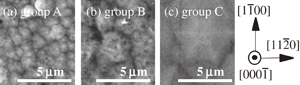
Fig. 3. Plan-view SEM images of InGaN films of (a) A, (b) B, and (c) C samples (on the sapphire substrate with a miscut angle of 0.9°).
Download figure:
Standard image High-resolution image3.3. Validity of the atomic-scale view of GaN template surface
It is found here that the effect of the substrate miscut angle for the coherently grown B and C samples is completely different from that for the group-III-polar grown InGaN, in which the In content monotonically decreased with increasing miscut angle.4–6) Prior to the discussion of this In incorporation issue, firstly the microscopic step structures on the GaN template are discussed here. As mentioned before, sapphire substrate surfaces have a misorientation around the [ ] axis. Accordingly, the GaN layers have a misorientation around the [
 ] axis and the surfaces should incline toward the [
 ] axis. However, a closer look at the GaN template II surface morphologies in Fig. 4 shows local atomic steps that run perpendicular to the [
 ] and [
 ] directions on average, i.e., two sixfold
  directions, instead of the [
 ] direction. Actually, these orientations are consistent with the frequently observed step directions around hexagonal hillocks shown in Fig. 3(c) and those described in Ref. 16. Therefore, it is expected that each step will form a zigzag shape on a larger scale, where steps perpendicular to the [
 ] and [
 ] directions appear alternately, as observed on left-hand side of Fig. 4(c), with the resulting macroscopic surface inclination being toward the [
 ] axis, which is consistent with the ideal step orientation introduced by the miscut of the substrates. If the step height is assumed to be identical to the lattice constant c of the wurtzite structure,16) the mean distance along the [
 ] direction between neighboring steps is estimated to be 74, 37, 33, and 27 nm when the miscut angles are 0.4, 0.8, 0.9, and 1.1°, respectively. These distances are in fairly good agreement with the observed distances in Fig. 4. This shows that the miscut angle of the substrate definitely has considerable effects on the atomic steps of the GaN template surface, on which evenly spaced atomic steps are observed, as shown in Fig. 4. Also, the above discussion holds true for both templates I and II even in the presence of step bunching, since it is also expected that the observed macrostep also will consist of a bunch of the above zigzag atomic steps distributed with quite a small interval.
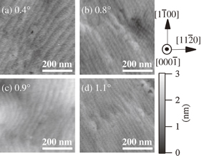
Fig. 4. AFM images of GaN template II grown on sapphire substrate with miscut angles of (a) 0.4, (b) 0.8, (c) 0.9, and (d) 1.1°.
Download figure:
Standard image High-resolution image3.4. Roles of the step edges and terraces in the indium incorporation
The B and C InGaN layers grown on the GaN templates are presumably affected by the substrate miscut angle, at least in the initial stage of their growth before hillocks and/or irregularities are formed. Therefore, to explain the difference in the miscut angle dependence of In incorporation between the N- and group-III-polar InGaN layers, here we show a cross-sectional schematic illustration of the step-and-terrace structures for each polarity in Fig. 5. In Fig. 5, group-III atoms without bonds indicate possible incorporation sites. It is reported that the step height of a N-polar surface is c, while that of a group-III-polar surface is c/2.16) The atomic structures are drawn using VESTA.17)

Download figure:
Standard image High-resolution image
Fig. 5. Schematic atomic arrangement of (a) N-polar and (b) group-III-polar step edges toward a-plane. Surface H atoms are not shown (see the text).
Download figure:
Standard image High-resolution imageUnder our growth conditions, the growth rate is limited by the total concentration of group-III precursors.18) In other words, there are sufficient N-precursors in ambient that are not adsorbed or incorporated into a crystal. Therefore, the NHn (n = 1, 2, 3) radical, after the attachment of group-III atoms immediately covers, the growth surface, and it is probable that a model with a nitrogen-stabilized-growth surface can be adopted in the case we will discuss below.19) In the case of InGaN growth, the bond strength between In and N is weaker than that between Ga and N, as expected from a higher nitrogen-equilibrium vapour pressure of InN than of GaN.20) Therefore, what determines the In incorporation efficiency in InGaN growth is the rate of replacement of In atoms by Ga atoms on the growth surface. To prevent the In atom replacement, a site with the higher number of bonds from the surrounding N atoms has distinct advantage because a higher number of bonds can hold In atoms tightly and prevent their detachment.
In the case of the N-polar surface, it is predicted by theoretical calculations that 3/4 of the surface N atoms are terminated by H and 1/4 of the surface N atoms have a lone pair of electrons on the terrace under MOVPE atmosphere,21) while the group-III atoms at the step edge adsorb NHn, where n is varied to satisfy the electron counting rule. Then the next incoming group-III adatoms can be caught between this adsorbate and the surface N below it instead of H atoms, as shown in Fig. 5(a). Therefore, group-III atoms are incorporated mainly at step edges, not on the terrace of the N-polar surface. This is consistent with the fact that the MOVPE growth rate on N-polar surfaces is much lower than that on group-III polar surfaces, unless hillocks are formed.16) When the growth rate increases with the step density, the In incorporation efficiency also increases because In can be covered by N atoms rapidly before they are replaced by Ga atoms.
On the other hand, in the case of group-III-polar growth, it is predicted by the theoretical calculations that 3/4 of the surface Ga atoms will be terminated by NH2 and 1/4 of the Ga atoms will be terminated by NH3 on the terrace under MOVPE atmosphere,22) while the step edge is being terminated by NHn. Therefore, each of the group-III atoms can be caught by three N adatoms on the terrace and the nucleation of two-dimensional islands is possible, as shown in Fig. 5(b). It is therefore considered that the effects of the step density and substrate miscut on group-III incorporation are smaller on group-III polar surfaces than on their N-polar counterparts.
3.5. Miscut angle dependence of the indium incorporation efficiency
Finally, to confirm the validity of the above models, it is necessary to know the initial surface morphology of the underlayers just before the InGaN growth. In this study, we have observed both the macroscopic and microscopic surface morphologies of GaN templates by OM and AFM. Figure 6 shows OM images of GaN templates I and II. Note here that GaN templates without hexagonal hillocks were obtained owing to the introduction of the vicinal substrate.9) However, giant or macroscopic steps due to surface step bunching become pronounced in the higher-miscut-angle region, as shown in Figs. 6(b) and 6(c), and 6(f) and 6(g), respectively. Therefore, we considered these macroscopic steps as the origin of the enhanced In incorporation, and estimated the average distance between neighboring macroscopic step edges by AFM. Figure 7 shows the In content of InGaN plotted as a function of the average interval of macrostep edges. It was found that the In content increased with increasing macroscopic step density, which is the inverse of the macrostep period. Note that the tendency was only observed in the series of the B and C samples grown coherently on the GaN template. This result is in good agreement with the model shown in Fig. 5(a).

Fig. 6. OM images of GaN templates I and II grown on sapphire substrate with miscut angles of (a) 0.6, (b) 0.9, and (c) 1.0°, and (d) 0.4, (e) 0.8, (f) 0.9, and (g) 1.1°, respectively.
Download figure:
Standard image High-resolution image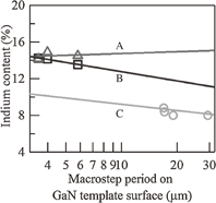
Fig. 7. In content as a function of macrostep period.
Download figure:
Standard image High-resolution image
4. Conclusions
The effect of the c-plane sapphire-substrate miscut angle around its a-axis on the In content of N-polar InGaN/GaN was investigated. The In content of the coherently grown InGaN samples increased with the substrate miscut angle, while the relaxed film grown via the island growth mode exhibited no distinct change in the In incorporation rate. The former result is opposite of that in the group-III-polar case. To explain the difference, we introduced a model based on the theoretically predicted surface structures during MOVPE growth. From the model, it is considered that two-dimensional nucleation on the terrace is rare in the case of N-polar growth. Therefore, the growth rate and In content increase with the step density, which is proportional to the substrate miscut angle. As a confirmation of the above model, the initial surface morphologies of the GaN templates just before the InGaN growth were observed. It was found that the In incorporation rate directly correlates with the macroscopic (giant) step density, which indicates a bunch of atomic-scale step edges, consistent with the above simple model.
Acknowledgements
K. Shojiki is supported by a Grant-in-Aid for JSPS Fellows Grant Number 25·10877. This work was partly supported by a Grant-in-Aid for Young Scientists (A) Grant Number 23686010.