
Abstract
Electron microscopy (EM) techniques are used to investigate the microstructure of ultrathin carbon layers obtained by focused ion beam induced deposition (FIBID). The investigation determines the crystalline structure, chemical bonding and elemental contents of FIBID-C materials. The effect of a thermal treatment to the ultrathin C films is analyzed. As-deposited FIBID-C is a metastable material transforming at mid-high temperatures. Evidence of its graphitization by metal catalysis is presented. Understanding of the heat transformation and crystallization is established based on the observations. Specifically, carbonization, H desorption decomposition, and graphitization, driven by high temperature metal-induced crystallization, are the identified processes. Demonstration of the graphitization of ultrathin FIBID-C enables a strategy towards graphene integrative planar technologies.
Export citation and abstract BibTeX RIS
1. Introduction
Since the isolation of single-atom thick carbon layer,1) the graphene, a revolution concerning its research occurred in many fields for the advance in both its technology, toward applications, and science, for its purely fundamental understanding.2) Yet universal, highly controlled graphene synthesis and integration which would imminently bring the nanomaterial massively into the market as products and devices exploiting and benefiting from graphene top electronic, mechanical and chemical properties are not available. Most probably a single solution does not exist and full awareness of the potential of novel two-dimensional (2D) materials has just started to come out.3,4)
Imaging techniques applied to graphene, such as electron microscopy, have played a major role to study its properties and to determine its characteristics. Nevertheless, the protagonist character of electron microscopy (EM) — specifically, the transmission electron microscopy (TEM) — is indissoluble to nanostructured materials, fact being most represented by the very discovery of carbon nanotubes (CNT).5)
Presently TEM is in some way routinely used as an imaging tool, to simply show the products obtained by the different graphene synthetic processes.6,7) For example, graphene layers are transferred to the conventional grids for TEM observation after the metal etching of the catalyst used in chemical vapor deposition (CVD) graphene growth.8) The TEM technique is itself a way to test the physical properties of graphene. Here9) the mechanical stability of graphene and its connection with the material atomic defects could be probed. Correspondingly, the effect of the energetic electron beam on CNTs and other graphitic nanostructures had been early reported.10,11) Since then, a number of more sophisticated TEM-based techniques have been applied to reveal graphene characteristics, such as the crystal grain size. Applied to few layer graphene it can give valuable information about the graphene layers stacking and rotational misalignment,12) which is especially important in terms of the electronic states and often manifested by scanning tunneling microscopy.13)
TEM advanced modes, such as electron energy loss spectroscopy (EELS), allow the determination of specific, fundamental, and relevant, properties of graphene. The work of Hairi et al.14) shows and comprehends the distinctive EELS spectra obtained when comparing graphene against few layer graphene data. Additionally, the actual trend in TEM is focused towards atomic resolution imaging. As an example, cutting-edge TEM spectroscopy is developed to reveal the atom-by-atom electronic states at the graphene edges in Ref. 15, as the boundaries and local atomic configurations would determine the performance of graphene electronic devices. In most of these cases, in plane observation is used.
In other circumstances, cross sectional observation of graphene layers is useful. For instance, it is a convenient way to study the graphene formation mechanism, as occurring in the epitaxial graphene growth by the thermal decomposition of SiC7) or to correlate the deposition of graphene by transition metal catalytic growth,16) which shows similarities, but it is not always equivalent, to the CNTs growth studies.17) Off-plane investigation approaches connect directly with the necessity to prepare specimens which are transparent under the electron beam.
Focused ion beam (FIB) is a most suitable tool for the TEM specimen fabrication purpose. The local and controlled milling capability of the fine energetic ion probe enables the strategic removal of material, thinning of the lamella and its transfer to a suitable grid for the TEM imaging.18,19) If correctly executed, any FIB-based processing and nanostructure fabrication can preserve the integrity of the sample material or properly realize the intended devices.20,21)
The use of the nanometer size ion beam can be complemented by some gas species to enhance its etching, material removal, capabilities.22) Otherwise, the combination of the ion beam and gas species can be used to promote layer and material deposition using the gas molecules as a precursor.23) The latter additional operational capability is the so-called focused ion beam induced deposition (FIBID). The FIBID technique is typically used for the safe relocation of the thin specimen to the TEM fitted grid using some needle operated by a microprobe. In other cases, FIBID, or its electron beam counterpart the focused electron beam induced deposition (FEBID), can be used as a precise nanopatterning tool of device structural and functional materials.24)
As we presented in a previous publication,25) the current FIBID approach explores another practical application of the FIBID-C layers. It is a preliminary and exploratory demonstrator toward the feasibility of an alternative application26,27) technology for graphene-like and related C materials. The concept of the whole strategy would be stated as addressing the following points: 1) the use of a finite carbon source, 2) a priori defining the location, 3) the patterning capability to enable shape design of the final carbon features, and 4) to avoid transfer to a dielectric or practical substrate. The obtaining of the crystalline materials is based on the (metal-assisted) thermal transformation of FIBID ultrathin carbon patterns.
In the present communication, we focus on the physical aspects of the FIBID-C materials and derived materials to comprehend their synthesis mechanisms and thermodynamics of the process based on their morphological, structural, and electronic characteristics as understood from an EM-based investigation28) of the applied processing steps. As one of the key aspects of this paper, the crystallization mechanism is attributed to the specific characteristics of the as-deposited ultrathin carbon layers, which directly derive from the use of the ion beam. The technological approach ultimately could be exported to generate some sophisticated version, even based on other ion beams and selected precursor materials, as well as including advanced patterning strategies, such as pursed in Refs. 29 and 30.
2. Experimental methods
2.1. Processing: FIBID-C and thermal treatment
FIBID-C features have been patterned on top of 500-nm-thick oxidized-Si wafers. After a simple surface chemical cleaning of the support chips, the patterning is performed using a commercially available dual beam system. The Ga+ beam conditions are 30 kV and beam current 300 pA, irradiation being done under normal incidence. The carbon precursor is phenanthrene (C14H10) molecules, vaporized at 65 °C and injected close (300 µm) to the incidence point of the (electron and) ion beam(s) upon the sample surface via a gas injection system (GIS) nozzle. The whole fabrication process for metal-induced FIBID-C crystallization has been previously described in Ref. 25. Additional data will be published in Ref. 31. More detailed explanation of the FIBID-C deposition and its processing, as well as FIBID technique related aspects, can be found there.
All samples used for the TEM studies, called Case 1, Case 2, and Case 3, have been patterned under the same conditions. FIBID-C nominal thickness is 10 nm for all three cases, which is controlled and can be determined by the deposition time at a fixed aperture/beam current. Only post-deposition processing differs. Respectively, Case 1 corresponds to as-deposited FIBID-C; Case 2 is heat-treated FIBID-C; Case 3 is analogous to Ref. 25, thus, Ni foil-assisted thermal treatment of the FIBID-C ultrathin, patterned layers. For Case 2 and Case 3, the heating conditions are 975 °C lasting for 30 min. An IR lamp furnace operated in vacuum is used for the thermal treatment. The Ni catalyst is a polycrystalline high purity material, structured as a 10-µm-thick foil.
2.2. Characterization: Electron microscopy and Raman scattering
For the TEM specimen preparation, conventional FIB-based fabrication is applied, once fully processed, for each sample type, thus, after thermal treatment if applied (Cases 2 and 3), not for Case 1. A Pt layer is deposited onto the sample surface to protect the FIBID-C patterns during the milling routine of fabricating the cross-sectional TEM-transparent specimens. Lamellas were prepared by a Hitachi FB2100 FIB system. FIBID-C specimens were roughly milled at 40 kV and finally, thinned at 10 kV.
EM-based characterization includes high resolution TEM (HRTEM), EELS, and elemental maps by scanning TEM energy-dispersive X-ray spectroscopy (EDX). The microscope is a JEOL JEM-ARM-200F. Electron beam is operated at 80 kV to prevent knock-on atomic damage of crystalline C nanomaterials, as reported in Ref. 10, and to reduce eventual electron beam induced phenomena on the FIBID-C (metastable) materials, particularly Case 1. The EELS spectra were acquired using TEM mode with an energy resolution of 0.6 eV. Some diffraction analysis had been applied as well, but the characteristics of the samples, the transversal view of the ultrathin layers and imperfect crystallinity, were not favorable to obtaining clear diffraction patterns (hence, not shown).
Instrument and measurement conditions for micro-Raman scattering are equivalent to previously reported.25) Laser excitation wavelength of 532 nm and a spot size of >2 µm have been used.
3. Results and discussion
3.1. Morphological characterization
Figure 1 is a HRTEM micrograph of an as-deposited FIBID-C layer (Case 1). The cross sectional view of the FIBID-C exposes the evenness and smoothness of the as-deposited C layer. No impurities are observed (nor unambiguously detected by EDX, see more details below). The most important aspect to note is that the uniform granular texture, no contrast domains are seen, does not show any structural ordering within the solid layer. This corroborates that the precursor molecules, phenanthrene, do not keep their integrity as expected by the use of FIBID, a FIB-based growth process rooted on the ion-molecule collisions23) and do not pile up in an ordered or self-assembling manner. The resulting material is constituted by an amorphous material, where chemical bonding and composition changes of original precursor molecules are assumed and reported.32,33) In summary, as-deposited FIBID-C is an atomically disordered compact material resulting from the crystalline distortion and certain bonding of the precursor molecules. The mechanical vibrational properties of pillar structures fabricated with an equivalent method and analogous precursor indicate that the as-deposited FIBID-C material is amorphous (non-crystalline), where diamond-like carbon (DLC) (sp3) bonds dominate.34) Based on this, as-deposited FIBID-C may be denser than common (porous) amorphous carbon materials and, instead, show more similarities with thin layer DLC materials35) deposited by ion beams36) or plasma CVD.37) Although the SiO2–C interface mixing caused by the use of the ion beam for the amorphous layer deposition is apparent, (the thickness of) the C layer can be distinguished as to be able to determine its value. Being approximately of 10 nm, therefore, matches the nominal thickness, which is based on the processing conditions (here, deposition time and beam aperture) and as it has been determined by an atomic force microscopy-based calibration of the deposition rate.31)
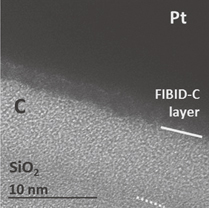
Fig. 1. Cross sectional HRTEM of as-deposited FIBID-C (Case 1).
Download figure:
Standard image High-resolution imageThe transformation resulting from the metal-assisted thermal treatment of the FIBID-C layers (Case 3) is illustrated in Fig. 2. This HRTEM compound image is a zoom of the area marked in the inset TEM image. The amorphous as-deposited FIBID-C layer shows now an obvious layered morphology (>10 layers) which is oriented roughly parallel to the sample support, the SiO2 substrate. Therefore, observation of graphitization confirms the results of Raman scattering characterization presented in Ref. 25. Although the existence of inclusions (Ni, see EDX discussion below) is clear, its direct and unambiguous correlation to the evidenced graphitization cannot be stated as the crystallization is also found apart from those inclusions. This point can be appreciated for example in the image right side area, but more examples of graphitized materials are included in Fig. 3, Note 1. Another indication related to the Ni contribution is the fact that, quite the opposite, evidence of layering formation does not always occur on top of the inclusions, as it can be seen in the left side edge of the Fig. 2 micrograph. No evidences have been found to attribute the observed layered structure to CNT formation, confirmed by the absence of tiny Ni catalyst nanoparticles.
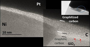
Fig. 2. Cross sectional HRTEM of metal-assisted heat treated FIBID-C (Case 3). No evidences have been found to attribute the observed layered structure to CNT formation, as e.g., understood by the nonexistence of tiny Ni nanoparticles.
Download figure:
Standard image High-resolution image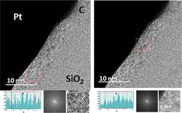
Download figure:
Standard image High-resolution image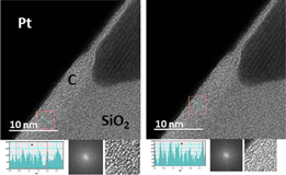
Fig. 3. Note 1: As seen in the first and second images (same location), graphitization can be found apart from inclusions. Note 2: Interlayer space analysis of four graphitized areas. Corresponding measured C layer to C layer separations from each red marked area are, from left to right (in Å): ∼2.9, ∼2.8, ∼3.3, and ∼2.9.
Download figure:
Standard image High-resolution imageIn the right half image region, another feature can also be observed. Ultimately, incomplete graphitization of the FIBID-C is found next to the SiO2–C interface. While the SiO2 layer and C layer can be here easily distinguished, no extended atomic carbon ordering, i.e., graphitic carbon formation, is observed. However, ∼1 nm long chains are visible in this region (red arrows in Fig. 2) which may be antecedents of extended graphitization.38)
Zoom out TEM observation and inspection of other areas (not shown) present similar characteristics: formation of graphitic carbon, existence of inclusions, heterogeneous and partial C crystallization. The existence of contrast changes in TEM are a good measure of defects and non-uniformities on crystalline structures.39) In addition to a certain increase of the oddness of the FIBID-C surface, a decrease of the layer thickness can be observed and estimated in ∼20–30% thickness reduction.
A similar trend concerning as-deposited FIBID-C thickness reduction is obtained for the thermal treated FIBID-C, Case 2, i.e., thermally treated without using any metal, e.g., Ni foil (Fig. 4). It accounts for a thickness layer decrease of ∼15–25%. The loss can be expected when graphitization occurs (solid state matter), but the fact that it is also found for Case 2 is an indication of a certain elemental composition change, for instance, partial decomposition by H desorption due to thermal treatment as reported in Refs. 33 and 40.

Fig. 4. Cross sectional HRTEM of heat treated FIBID-C (Case 2).
Download figure:
Standard image High-resolution imageCollecting the observations, the most important fact to mention is that the graphitic conversion of FIBID-C, the transformation into a layered C structure, is never observed for merely heat treated samples. It is clear that no crystalline material is obtained and a granular texture appears more visible in Case 2 than in the non-graphitized portions of Fig. 2 layer (Case 3). As studied from the Raman scattering spectra of thermal annealed FIBID-C,25) in spite of a certain formation of aromatic rings as understood from the distinguishability of D peak and the shrinking of G peak, the broadness of the D and G bands indicates a very low graphitization degree and only incomplete "crystal" relaxation.41,42) Another manifest feature is that the SiO2 layer top surface is recovered after thermal treatment, similarly to the previous Case 3, as the C–SiO2 interface can be easily seen. Interface minor oddness and that of the C layer can probably be correlated. TEM image contrast is fairly uniform throughout the layer.
3.2. Structural and chemical analysis
The morphological and structural direct observation by HRTEM has been complemented with EELS analysis. EELS low energy range informs about the atomic bonding.43) Separate low loss EELS spectra for Case 1, Case 2, and Case 3 are shown in Fig. 5. Characteristic plasmon excitations, corresponding to both bulk and surface modes of the valence electrons, can be observed for the different graphitic materials.44) As depicted in Fig. 5, a peak resulting from the π-excitation plasmon loss is clearly promoted for the metal-assisted thermally treated FIBID-C (Case 3), whereas is absent for the as-deposited FIBID-C (Case 1) and significantly lower for heat treated FIBID-C (Case 2). Respect to the signature value of graphene, ∼4.7 eV, the Case 3 peak position located at ∼7 eV is shifted towards higher energies, which is a characteristic property of graphite.44) This result is in total agreement with the typical Case 3 Raman spectrum25) and the observed multilayer structure, shown in Fig. 2. For predominantly-sp3 materials, such as DLC or diamond, the lack of this peak is anticipated.44)

Fig. 5. EELS spectra for Case 1, as-deposited FIBID-C; Case 2, thermal treated FIBID-C; and Case 3 metal assisted thermal treated FIBID-C.
Download figure:
Standard image High-resolution imageThe evolution of the plasmon loss peak for π + σ is different. A broad peak between 20–40 eV is recorded for the three cases, like commonly found in the literature for graphite, tetrahedral amorphous C (ta-C) or diamond.45) A plasmon loss centered about 24 eV is an indication of the sp3 carbon bonds, consistent with recorded spectra of Case 1 and Case 2 (Fig. 5), but not always observed for so-called amorphous carbons.46) Comparing again with single and few layer graphene, the energy shift toward higher energies observed for Case 3, peak at 24 eV plus peak at 27 eV, is an indication of the formation of graphitic carbon,37) while single layer graphene would be typically observed by a peak at ∼15 eV.39,44) The convoluted peak can be explained by the coexistence of graphitized and non-graphitized FIBID-C, as seen in Fig. 2. Easier appreciation of the shift indicative of graphite tendency for Case 3 material can be found in Fig. 6, where the three spectra are shown all in one, using a π + σ peak-intensity normalization.
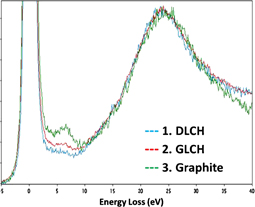
Fig. 6. Composed EELS spectra for the three types of analyzed materials, Case 1, Case 2, and Case 3. Graphite signature is obtained for the case of metal-assisted thermal transformation of FIBID-C. DLCH, diamond-like carbon hydrogenated; GLCH, graphite like carbon hydrogenated.
Download figure:
Standard image High-resolution imageNot only for completeness, but because a few interesting features have arose, EDX analysis has been applied to the three types of FIBID-C materials discussed in this paper. Some exemplary mapping pictograph (Case 3) is shown in Fig. 7. The chemical identification of the plate-shaped inclusions, similar to the one observed in Fig. 2, indicates that they are composed of mainly Ni, which might be a precipitate from the Ni foil. Interestingly, the Ni plates, with sizes up to 100 nm in length and an average thickness of ∼25 nm, penetrate into the SiO2. In addition, they are located below graphitized FIBID-C, which suggests that some Ni moves towards the SiO2–C interface and precipitates. Thus, in some way the dissolved material due to thermal treatment is the Ni. In a strict sense, this feature shows incompatibilities, or in other words suggests particularities, respect the conventional graphene on Ni growth mechanism based on the C dissolution inside the Ni and precipitation upon cooling.47) Probably, only by in situ TEM, simultaneous TEM-heat treatment, could be elucidated the precise origin and dynamics of present phenomenon.48)
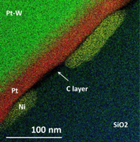
Fig. 7. EDX mapping of Case 3. Carbon film corresponds to the black layer sandwiched between Pt protection coating and SiO2 support. Ni nanoplates can be easily distinguished as well (yellow).
Download figure:
Standard image High-resolution imageAn additional kind of inclusions is occasionally found (not present in Fig. 7). They consist in ∼150 nm in diameter ball-like particles, which are embedded deep inside the dielectric SiO2 support. From EDX analysis they appear to be a nickel silicide compound. Some crystalline structure could even be observed. We hypothesize that nickel silicide formation results from a complex reaction of molten Ni and SiO2 perhaps promoted by some residual Ga atoms from the ion beam and the same presence of C. Again, conclusive thermodynamics involved in the metal-assisted thermal treatment of FIBID-C have not yet been determined and further investigation would be undertaken.49)
3.3. Transformation mechanisms
Derived from the profuse characterization and its analysis, two relevant aspects can be understood. First, considering the classification of amorphous carbons based on the ternary phase diagram in Refs. 37 and 49, Case 1, Case 2, and Case 3 materials can be classified. Case 1, as-deposited FIBID-C is a diamond-like carbon hydrogenated material (DLCH): high amount of sp3 bonding, significant H contents and disordered atomic distribution. Case 2, thermally treated FIBID-C would correspond to graphite like carbon with the possibility of remnant H contents [GLC(H)]: increase of sp2/sp3 ratio, partial decomposition, but no apparent structural atomic ordering. Finally, Case 3, metal-assisted heat treated FIBID-C are ultrathin layers of graphite-like or graphitic carbon, whose crystalline structure depends locally on the degree and depth extend of the graphitization. Nanographene nomenclature25) is thus valid.
More details on the variety of amorphous C materials and the necessity to identify them, as they present radically distinctive properties arising from structural (chemical bonding and atomic arrangement) and elemental contents (percentage of H, N, etc.) can be consulted in Refs. 36 and 49. Briefly, in Ref. 49 amorphous carbon family is understood based on a ternary phase diagram whose corners correspond to diamond, graphite and hydrocarbons. Respectively, this classification accounts for sp3, sp2, and H material contents. The intermediate materials make up the variety of the amorphous carbon materials, including DLCH, ta-C, GLCH, and so forth. The change from perfect sp2 configuration (graphite) can be described by three amorphization stages, as a compound non-linear dependence of 1) decreasing cluster size and 2) increasing percentage of sp3 bonds. Specifically applied to FIBID-C, some additional discussion of amorphousness and chemical bonding for the hereby discussed materials has been included in Ref. 50.
Secondly, the material transformation processes are identified and elucidations on the thermodynamics mechanisms involved can be inferred. The as-deposited FIBID-C layers are metastable under mid-high temperature treatments32,33,40) and its transformation includes two processes. Carbonization process is found, as a result of H decomposition of the deposited-amorphous phenanthrene molecules. Carbonization not only leads to a purer C material, but additionally implies the break of sp3 chemical bonds, which favors the formation of sp2 bonds, the C=C covalent bonding.38)
Additionally, the crystallization mechanism, the graphitization process, occurs only when metal-assisted heat treatments are applied. Although our FIBID-C graphitization method has not yet been uniquely clarified, but evidenced, strong arguments for considering surface metal-induced crystallization51) are indicated. This mechanism applies instead of, typically assumed, C dissolution into Ni and graphene formation by precipitation onto the Ni surface during cooling.47) We specifically attribute this particular behavior to the strength of the DLC bonds resulting from the deposition technique (FIBID) of the precursor material, the FIBID-C.33,35,36) The use of metal foil might also play a significant role as the direct C–Ni contact similar to the one obtained when using carbon and nickel layer deposition52) is not guaranteed in the present case. These two conditions may additionally prevent the activation of a massive C dissolution in Ni and precipitation mechanism.47) As an alternative, an actual metal-induced crystallization51) of the most superficial FIBID-C atoms implicitly provides the subsequently inner FIBID-C atoms with a higher degree of freedom, therefore lowering the energy required for their graphitization. As a result, an in-depth progressive crystallization mechanism could be occurring. The limited mobility is also determined by the already existing strong C=C bonds within the as-deposited FIBID-C.
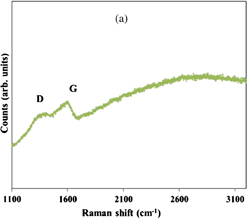
The remnant stress, or incomplete relaxation, of graphitized FIBID-C is most illustrated by an eventual reduced interlayer space of the graphitic carbon, ranging from ∼2.7 Å to, the standard, ∼3.35 Å for graphite. Four measurement examples are displayed in Fig. 3, Note 2. Compressed graphite, the graphitic carbon of reduced interlayer distance,53) as reported in the literature based on X-ray diffraction data, shows a similar reduction, for example, as a result of pressurization in the GPa range.54) A permanent lattice compression of graphitic C is attributed to the fractional conversion of π bonds (sp2) into σ bonds (sp3) bridging (thus, coexisting with) the original graphitic carbon layers.55) This aspect directly correlates and can be extrapolated to the EELS results shown in Figs. 5 and 6. The polycrystalline structure of Ni would also be a factor for a local non-uniform catalysis of the graphitization in a nanometer scale, which crystallization heterogeneity and material stress in this scale order are identifiable from the Raman spectra, as mentioned in Refs. 41 and 42 and provided in Fig. 8.
Download figure:
Standard image High-resolution image
Fig. 8. Representative Raman spectra of the same samples showed in (b) Fig. 4 for Case 2, thermal treated FIBID-C (a); and Fig. 2 for Case 3, metal-assisted thermal treated FIBID-C (b).
Download figure:
Standard image High-resolution image
4. Summary and conclusions
A profuse HRTEM, EELS, and EDX study has been performed to investigate the cross sectional microstructure of ultrathin carbon layers obtained by FIBID from a phenanthrene precursor (C14H10). The products of applying a thermal treatment and metal-assisted heat treatment to the FIBID-C have been analyzed. As-deposited FIBID-C is a metastable material that transforms under mid-high temperatures. Significant crystallization only occurs when metal catalysis, e.g., here, Ni foil, is used. Evidence of the graphitization has been presented and its correlation with the obtained typical Raman spectra established.
The investigation allowed determination of the materials crystalline structure, chemical bonding and elemental contents; so that the as-deposited FIBID-C, the thermal treated FIBID-C, and the metal-assisted thermal treated FIBID-C could be classified as DLCH, GLC(H) and graphitic carbon, respectively.
The comprehension of the transformation process and of the formation of crystalline material comprises two processes, carbonization and graphitization. Carbonization includes the FIBID-C layer decomposition by H desorption and reduction of sp3 bonds percentage. Graphitization implies a substantial reordering of the atomic carbons into a layered structure. Crystallization is a result of a metal-induced crystallization of superficial FIBID-C, which is made possible by applied high temperature, and the consequent mechanism occurring inside the FIBID-C layer.
The work not only demonstrates the fundamental and particular characteristics of the different FIBID-C materials, but reveals the specific aspects of the transformation mechanism, which are to a great extend exclusively derived from a particular approach, the use of FIBID technique and probably valid for other conventional methods based on ion beam-deposited ultrathin layers. Demonstration of the graphitization of ultrathin FIBID-C patterns directly grown on an insulating support is of remarkable importance from the point of view of the establishment of integrative graphene planar technologies.
Acknowledgments
Most of the experimental work was done during the post-doctoral fellowship of Dr. G. Rius at Toyota Technological Institute. The financial support of the Strategic Research Foundation Grant-aided project for Private Universities from the Ministry of Education, Culture, Sports, Science and Technology, Japan is acknowledged. We also appreciate the collaboration of Ph. D. Francisco C. Robles Hernandez of the University of Houston (U.S.A.) for some assistance in HRTEM data analysis.