Abstract
We have been attempting to use liquid silicon (Si) in a solution process to develop semiconductor materials. We chose cyclopentasilane (CPS) as the raw material, which can be converted to poly(dihydrosilane) by photoinduced polymerization. Poly(dihydrosilane) is mixed with an organic solvent to form Si ink. We fabricated not only intrinsic Si ink but also both n- and p-type doped-Si inks. In the solution process, coating and pyrolysis are essential for device development. The parameters of these processes and the quality of the resultant solid film strongly depend on the properties and behavior of liquid Si, including those of CPS, poly(dihydrosilane), and Si ink. Here, we clarified the structure and properties of CPS, the photopolymerization of CPS, the structure of the polymer [poly(dihydrosilane)] in solution, the criteria for forming a uniform polymer film on a substrate, and the pyrolysis of a polymer film to an amorphous Si film. We also evaluated the properties of the resultant amorphous films. The quality of a solution-processed film was inferior to that of a vacuum-processed film just after the pyrolysis; however, it can be improved to a device-grade film by hydrogen radical treatment. So far, the devices that we have developed with liquid Si include polycrystalline Si thin-film transistors (TFTs), single-grained Si-TFTs, and thin-film solar cells. For TFTs, their excellent properties have been demonstrated. In this review article, we introduce the development of solar cells using hydrogenated amorphous Si (a-Si:H) films for the p–i–n structure. We also show that the solution-processed a-Si:H solar cells exhibit 0.31–0.51% efficiency under AM-1.5G (100 mW/cm2) illumination.
Export citation and abstract BibTeX RIS
1. Introduction
Silicon (Si) is established as a necessity in the electronics industry. Among the three states of matter, only the solid and gaseous states of Si have been utilized: in the solid state, Si as a single-crystal Si wafer is used for semiconductor devices, and in the gaseous state, Si as a vacuum deposition source material is used for fabricating Si thin films. However, the liquid state of Si has never been applied industrially.
We have been researching liquid Si as a semiconducting liquid for use in so-called "printed electronics", in which all elements of an electronic device are printed. Although the term liquid Si is unconventional, we use it in a general sense, similar to a collective noun. Si ink is another term for this type of material, because it is applied in printing. We also use this term when liquid Si is specified as a material. Studies of liquid Si are now being conducted at several research institutes around the world. We have been using cyclopentasilane (CPS) as the starting material for fabricating liquid Si.1) At North Dakota State University in the US, researchers are synthesizing liquid Si using cyclohexasilane (CHS).2,3) Small Si particles, instead of molecules, can be used for synthesizing liquid Si. At Nanogram,4) Innovalight,5,6) and Kovio,7) in the US, Si suspension inks are being developed.
The reason for the lack of industrial use of liquid Si can be attributed to its difficulty of processing it to obtain semiconductor solids with good properties. When used as a semiconductor, a Si material with even a small amount of impurities is not acceptable. We must find a raw material that excludes impurities to the highest extent possible. Both siloxane and organosilane compounds are easy to handle; however, they do not exhibit semiconductor properties when converted to the solid state. No candidate except hydrosilane exists for liquid Si if we choose the molecular route. In the case of hydrosilane compounds, hydrogen can be removed by the pyrolysis, and a small amount of residual hydrogen can terminate defects in solid Si, leading to improved semiconductor properties. However, hydrosilane compounds are known to be extremely difficult to handle in nature. Although both silicon and carbon belong to group 14 (the carbon group), they differ from each other in terms of their hydrogen compounds. Hydrocarbon compounds are very stable in air, whereas hydrosilane compounds are very active in air. The latter cannot be handled in an oxygen atmosphere. Very sophisticated equipment is needed to guarantee a low (on the order of ppm) oxygen content. This type of equipment is not only expensive but also very complicated to use. Working efficiency is relatively low compared with processing in air when using this equipment. Furthermore, monosilane gasses which are generated through the pyrolysis process are very dangerous; thus, an attached device to remove it is necessary. Such difficulties might prevent researchers from conducting research on liquid Si. We have investigated many hydrosilane compounds both theoretically and experimentally, which can be converted to liquid Si of high purity and relative stability before we arrived at CPS. CPS has a boiling point (194 °C) higher than that estimated from its molecular weight. Its higher boiling point equates to its good stability. Moreover, it was found that CPS is converted to poly(dihydrosilane) by UV irradiation.1) Poly(dihydrosilane) is more desirable for liquid Si in terms of stability and processability than the monomer.
In this review article, we introduce a series of our studies of liquid Si. The first topic covers CPS and Si ink from CPS. The next topics cover the coating with liquid Si to prepare a Si polymer film on a substrate and its conversion to a solid Si film by the pyrolysis. The quality of the resultant films is also discussed. The final topic covers device fabrication.
2. CPS and liquid silicon formation from CPS
2.1. CPS and liquid silicon
CPS can be synthesized by the three-step reaction shown in Fig. 1. This is called the Kipping method.8–10) In our experiment, CPS has been synthesized by the same reaction as follows. Diphenyldichlorosilane was added to a stirred suspension of lithium in tetrahydrofuran, and the resulting mixture was stirred and poured into cold water. The resultant precipitate was collected by filtration, washed with water, dried in vacuum, and recrystallized to give a white powder (decaphenylcyclopentasilane). Its suspension and aluminum chloride in cyclohexane were mixed and stirred at room temperature with the bubbling of dry hydrogen chloride gas to give decachlorocyclopentasilane. The remained hydrogen chloride was removed by N2 bubbling from the solution. The solution of decachlorocyclopentasilane in cyclohexane was added dropwise to a suspension of lithium aluminum hydride in diethyl ether at 0 °C, and the resulting mixture was stirred for 12 h and then filtered. The filtrate was concentrated, and the residue was distilled under reduced pressure to afford pure CPS as a colorless liquid. The properties of the CPS are listed in Table I. Note that CPS has a relatively high boiling point, indicating a stable molecule to handle.
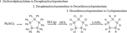
Fig. 1. The synthesis route of CPS.
Download figure:
Standard image High-resolution imageTable I. Properties of CPS.
| Molecular weight (g/mol) | 150 |
| Boiling point (°C) | 194 |
| Melting point (°C) | −10.5 |
| Refractive index | 1.691 |
| Specific weight | 0.963 |
| Band gap (eV) | 6.5 |
| Surface tension (mN/m) | 32.5 |
| 1H-NMR (ppm) | 3.25 (TMS) |
| 29Si-NMR (ppm) | 106.9 (TMS) |
In order to determine the exact structure of the CPS molecule, we have conducted a computational study using ab initio and density-functional methods.11) The calculations were based on Hartree–Fock theory, Mollet–Plesset perturbation theory, and density-functional theory (DFT). The geometrical structures of CPS were optimized within the given symmetry point group. After different structures of Si5H10 with different symmetries were analyzed, three stable structures of CPS were determined by our calculations, namely, planar (D5h), envelope (Cs), and twist (C2), which are shown in Fig. 2. The results of our calculations at all theoretical levels employed show that the twist structure is the most stable structure for CPS, and that the two other structures of CPS, i.e., twist (C2) and envelope (Cs), have similar energies at all the theoretical levels employed (the difference between their energies is on the order of 1.0 meV). The relative energies of each structure are summarized in Table II. These results are in good agreement with the results of previous theoretical studies.12,13)
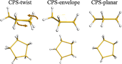
Fig. 2. CPS structure with geometries optimized with B3LYP/cc-pVTZ: planar (D5h), envelope (Cs), and twist (C2).
Download figure:
Standard image High-resolution imageTable II. Energy comparisons between twist structure and others. (in meV).
| Hartree–Fock | PBE (GGA) | B3LYP (HB) | MP2 | |
|---|---|---|---|---|
| Twist | 0 | 0 | 0 | 0 |
| Envelope | +0.03 | +0.01 | +0.03 | +0.03 |
| Planar | +60.79 | +61.20 | +53.65 | +60.58 |
2.2. Polymerization of CPS
Si ink is a mixture of poly(dihydrosilane) and an organic solvent. CPS can be converted to poly(dihydrosilane) by ring-opening polymerization, which occurs when UV light is irradiated to CPS. Figure 3 shows the optical absorption spectra of CPS just after distillation, CPS kept at 50 °C for 30 min after distillation, and poly(dihydrosilane). We usually use UV light of 365 nm wavelength; however, CPS just after distillation does not absorb light of 365 nm wavelength. Hence, it is interesting to investigate whether it is polymerized by the UV light that it cannot absorb. (This had been mystery for a long time.) We happened to observe that immediately after distillation, CPS is difficult to polymerize by UV light of 365 nm wavelength. In contrast, after some period at room temperature after synthesis, CPS can be polymerized at a much higher rate. We confirmed that a small amount of poly(dihydrosilane) can be formed in CPS by thermal polymerization. As shown in Fig. 3, poly(dihydrosilane) absorbs UV light of 365 nm wavelength. Figure 3 also shows that CPS kept at 50 °C for 30 min after distillation tends to absorbs longer-wavelength UV light than CPS immediately after distillation. These facts suggest that CPS polymerization is a two-step process: (1) poly(dihydrosilane) absorbs UV light, and its energy is transferred to CPS, and (2) the transferred energy is used for the ring-opening polymerization of CPS. This mechanism is just a presumption, and a more detailed study is needed.
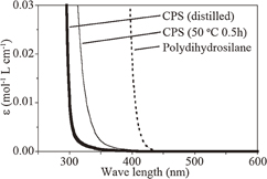
Fig. 3. Absorption spectra of liquid Si materials: CPS just after distillation, CPS kept at 50 °C for 30 min after distillation, and poly(dihydrosilane).
Download figure:
Standard image High-resolution imageIn order to determine the polymerization behavior, we characterized the molar mass distribution and structure of poly(dihydrosilane) by size-exclusion chromatography (SEC) combined with multi-angle laser light scattering (MALLS) analysis and viscometry (SEC-MALLS-viscometry).14) The SEC-MALLS system, viscometer, and refractive index (RI) detector were connected in series by stainless-steel tubes, as shown schematically in Fig. 4. An injector was set in the glove box. Readings of the excess Rayleigh ratio R(θ) at a scattering angle θ, specific viscosity ηsp, and RI response were acquired every 0.5 s during elution. A Shodex KF-805 column was used with a guard column attached to it. The molar mass (M) and root-mean-square radius (radius of gyration, Rg) were estimated using a Guinier–Zimm plot. The intrinsic viscosity [η] was determined by calculating ηsp/c directly for each elution volume. Here, c is the concentration of the solute [poly(dihydrosilane)]. For the analysis of the polymer structure, we adopted the sphere model, which is based on the viscosity theory of colloidal particles, to analyze the molar mass dependence of [η].15) In this model, [η] is described as

where Rh is the viscosimetric radius and NA is Avogadro's number. Starting from Eq. (1), we describe the scaling behavior of [η] vs M.

Fig. 4. Schematics of sample preparation and the SEC-MALLS-viscometry system. Within a glove box under an inert atmosphere (O2 concentration 0.5 ppm, dew point 75 °C), poly(dihydrosilane) was synthesized by the UV irradiation of CPS. The photographs indicate the change of the liquids from CPS to poly(dihydrosilane). The sample preparation and SEC-MALLS-viscometry measurement were conducted at 25 °C. Reproduced with permission from Ref. 14. Copyright © 2012 Elsevier B.V.
Download figure:
Standard image High-resolution imageFigure 5(a) shows the RI intensities for four samples synthesized with irradiation times of 0, 30, 60, and 240 min. The sample subjected to no irradiation (0 min) corresponds to CPS, and the inverted peak at a elution volume of 13 mL marks the end of sampling. The RI chromatogram for CPS exhibits a sharp peak at an elution volume of 12 mL. The spectrum for the sample with the 30 min irradiation time exhibits a broad peak at the lower elution volume in addition to the weak CPS peak. For the sample with the 60 min irradiation time, the broad peak at the lower elution volume grows significantly, whereas the CPS peak disappears. This suggests the completion of CPS photo-polymerization within 60 min of irradiation.
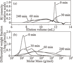
Fig. 5. SEC-MALLS result for CPS and poly(dihydrosilane) synthesized with irradiation times of 30, 60, and 240 min dissolved in cyclohexene at 25 °C. (a) RI intensity. (b) Molar mass distribution. Reproduced with permission from Ref. 14. Copyright © 2012 Elsevier B.V.
Download figure:
Standard image High-resolution imageThe differential molecular weight fraction of poly(dihydrosilane) is plotted as a function of the molar mass for the four samples in Fig. 5(b). The sample with the irradiation time of 0 min has a sharp peak at a molar mass of 150 g/mol, confirming the existence of CPS. Hence, the decrease in the intensity of the peak at 150 g/mol indicates how the molecular weight distribution spreads out when CPS is converted into poly(dihydrosilane) during the first 60 min of irradiation. The molar mass for poly(dihydrosilane) ranges broadly from 102 to 106 g/mol. The molar mass distribution changes significantly for the samples with irradiation times of up to 60 min, however, minor changes in the molar mass distribution are observed for the samples with irradiation times longer than 60 min.
2.3. Polymer structure in a solution
Here, we explore the structure of poly(dihydrosilane) on the basis of the scaling behaviors of [η] and Rg.14) Logarithmic plots of [η] vs M and Rg vs M for the sample with the irradiation time of 240 min are shown in Figs. 6(a) and 6(b), respectively. These plots exhibit a scaling feature, which was fitted by the linear functions described in Eqs. (2a) and (2b):


The scaling relation [η] = KMα is known as the Mark–Houwink–Sakurada equation.16) The data fitted by Eq. (2a) was in good agreement with the scaling relation. The solid line in Fig. 6(a) was fitted to [η] between 103 and 3 × 10⁶ g/mol, whereas the solid line in Fig. 6(b) was obtained by fitting Rg between 1.099 × 10⁶ and 4.457 × 10⁶ g/mol. Here, we focus on the fitting of [η] vs M and interpret the scaling behavior on the basis of the sphere model.15) Since [SiH2] (mass Mm = 30.102 g/mol) is considered to be a monomer unit of poly(dihydrosilane), the degree of polymerization (number of monomer units: N) of a polymer with molar mass M is given by N = M/Mm. Thus, the radius of gyration may be written as

where a denotes the "effective length" of [SiH2]. By substituting Eq. (3) into Eq. (1) and by using the parameter ρ = Rh/Rg, the Mark–Houwink–Sakurada equation of [η] = KMα is obtained, where α = 3ν − 1 and the coefficient K is given by

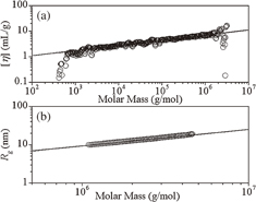
Fig. 6. Log–log plots of (a) [η] vs M and (b) Rg vs M for poly(dihydrosilane) with 240 min irradiation time dissolved in cyclohexene at 25 °C. The solid lines in (a) and (b) represent the linear fits of [η] and Rg, respectively. Reproduced with permission from Ref. 14. Copyright © 2012 Elsevier B.V.
Download figure:
Standard image High-resolution imageAccording to the present sphere model, the radius of gyration exponent is estimated to be ν = 0.402 for α = 0.206. Since ν = 0.410 in Eq. (2b), the agreement between the two results suggests that the sphere model for the viscosity can be appropriately applied to poly(dihydrosilane) with the monomer unit [SiH2]. If the poly(dihydrosilane) has a straight-chain structure, α should be in the range from 0.5 for Flory theta solvent to about 0.8 in a good solvent.16) However, the experimental value of 0.206 was much smaller than the cutoff value for a straight-chain polymer. Thus, we can presume that the poly(dihydrosilane) exists as a branched-chain structure.
With respect to the polymer shape, ρ = Rh/Rg gives a measure of the compactness of the molecule. By using Eqs. (2a) and (2b), ρ = 1.09 and ρ = 1.08 were determined for M = 1.099 × 10⁶ and 4.457 × 10⁶ g/mol, respectively. This also suggests that the poly(dihydrosilane) has a particle-like compact shape. For ρ = 1.09, by using Eq. (4) and K = 0.414 mL/g in Eq. (2a), a was estimated to be 0.145 nm. This value is in good agreement with the bond lengths between Si and H in various molecules.17,18)
It is concluded that poly(dihydrosilane) has a branched structure with a particle-like compact shape in cyclohexene at 25 °C. The existence of a branch point (SiH) was also predicted and confirmed with using 1H-NMR and Fourier-transform infrared spectroscopy (FT-IR).14)
3. Coating of Si ink
3.1. General remarks on Si ink coating
Once Si ink is synthesized, the next process involves coating the Si ink onto a desired substrate to make a poly(dihydrosilane) film. However, the formation of a film having homogeneous thickness is not straightforward. Immediately after Si ink is spin-coated, the solvent starts to evaporate, leaving behind the solute [(poly(dihydrosilane) in this case] on the substrate. During this stage, various types of dried solid patterns can be generated depending on the conditions of several aspects of the process. In some cases, a pattern such as a coffee stain forms, whereas in others, a multi-lined or dotted pattern appears. Uniform film formation is not always guaranteed.
Whether or not a good film is formed strictly depends on the behavior of the solute substance on the substrate during drying. To clarify the phenomenon, we investigated the stability of poly(dihydrosilane) films on solid substrates by a comparison between the observed micrographs at room temperature and the calculated values of the Hamaker constant (AALS) for the air/liquid/solid substrate. To efficiently compare the observations and AALS values, we selected five types of SiO2-based substrates (quartz, glass, and optical glasses A, B, and C) and a TiO2 substrate, because SiO2 is a popular substrate for silicon devices. Since the evaluation of the Hamaker constant is essential for determining the stability of polymer films, we adopted a simple spectrum method (SSM),19,20) which is adequate for a system composed of materials with different resonance frequencies, such as solids and liquids. For comparison, we also calculated the AALS values basis of the Tabor–Winterton approximation (TWA).21) We measured the optical parameters of several substances by an Abbe refractometry, ellipsometry,22) and FT-IR to determine the optical parameters in the London-dispersion (LD) spectra of the SSM.
3.2. Observations of liquid films
The formation of Si ink is as follows. The wavelength, intensity and irradiation time were 365 nm, 1 mW/cm2, and 60 min, respectively. Under these conditions, CPS was completely converted to poly(dihydrosilane) with a broad molar mass distribution (MW = 102–106 g/mol). Then it was dissolved in cyclooctane at 1.5 wt %. The film was coated on a solid substrate by spin-coating at 2000 rpm for 30 s. The resultant film thickness was 40 ± 5 nm. All processes were carried out in a glove box, where the oxygen concentration and dew point in the glove box were less than 0.5 ppm and −75 °C, respectively. First, the coated-liquid film was allowed to stabilize overnight at room temperature in the glove box; then, only the film surface was oxidized slowly to freeze the pattern in the film and deactivate it. The resulting film, which was regarded as a poly(dihydrosilane) film covered with a thin SiO2 layer, was taken out into the atmosphere, and the films were observed using an optical microscopy and SPM.
Figure 7 shows the micrograph of the poly(dihydrosilane) films coated on six types of substrates.23) The AALS value calculated by the SSM is noted on each image. Two types of prominent features, i.e., dot arrays and continuous figures, are observed in Fig. 7. A large number of cyclic dots in the liquid films on the quartz [Fig. 7(a)] and glass substrates [Fig. 7(b)] indicates film rupture. The separations among the dots in the film on glass were slightly longer than those among the dots in the film on quartz. The film on optical glass A showed two types of patterns: a patch like configuration of dots in Fig. 7(c) and a continuous pattern in Fig. 7(c'). In the present case, the two types of patterns coexisted in the same film. The images of the continuous films on optical glasses B and C and TiO2 [Figs. 7(d)–7(f)] were observed with high reproducibility. The profile of a single dot in the array was measured by SPM. Figure 8 shows a three-dimensional (3D) image obtained by atomic force microscopy (AFM) for a typical dot on the glass substrate shown in Fig. 7(b).

Fig. 7. Optical micrographs of poly(dihydrosilane) films on different substrates: (a) quartz, (b) glass, (c, c') optical glass A, (d) optical glass B, (e) optical glass C, and (f) TiO2. (c) and (c') images at different points on the same film. The AALS values calculated by the SSM are noted on each micrograph. The length of the bar in each image is 100 µm. Reproduced with permission from Ref. 23. Copyright © 2012 Elsevier B.V.
Download figure:
Standard image High-resolution image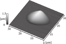
Fig. 8. AFM image of a single dot on the glass substrate in Fig. 1(b). The height and width of the dot are 1.31 and 18.45 µm, respectively. Reproduced with permission from Ref. 23. Copyright © 2012 Elsevier B.V.
Download figure:
Standard image High-resolution image3.3. Hamaker constant and coating property
We calculated the Hamaker constants based on the basis of the model shown in Fig. 9 by the SSM and TWA methods. The stability of the liquid film is determined by the free energy per unit volume F(L) = γSL + γLA + P(L), where L is the film thickness, γSL and γLA are the interfacial energies of the solid/liquid and liquid/air boundaries, respectively, and P(L) is the intermolecular interaction. When L is less than 1 µm, the energy term arising from gravity is ignored. For low-polarity materials, P(L) is dominated by van der Waals energy: P(L) = WALS. The WALS in the nonretarded Lifshitz theory24,25) is given by

According to this formula, a liquid film with AALS > 0 is stable, and that with AALS < 0 is unstable.26) The AALS values determined by the SSM (closed circles) and TWA (open squares) are plotted in Fig. 10 as a function of the refractive index of each substrate measured at 589 nm. The results for both the SSM and TWA indicate that the liquid films on quartz and glass are unstable (AALS < 0), and the liquid films on optical glasses B and C and TiO2 are stable (AALS > 0). The TWA and SSM gave opposite signs for AALS for the film on optical glass A. Our observed micrographs are consistent with the stability of the liquid films determined from AALS, except for the film on optical glass A. The stable films with AALS > 0 showed a continuous figure, while the unstable films with AALS < 0 showed an array of cyclic dots resulting from rupture. The observed image of the liquid film on optical glass A showed the so-called metastable state caused by the appearance of both a continuous figure and a patchlike configuration of dots. These results will provide basic and important information on how to prepare uniformed poly(dihyrosilane) films on solid substrates.

Fig. 9. Model of a liquid film on a solid substrate.
Download figure:
Standard image High-resolution image
Fig. 10. AALS vs n (refractive index of the substrate measured at 589 nm). Reproduced with permission from Ref. 23. Copyright © 2012 Elsevier B.V.
Download figure:
Standard image High-resolution image4. Conversion from polysilane to amorphous Si by pyrolysis
The formation of poly(dihyrosilane) films is followed by pyrolytic transformation to an a-Si:H solid film. We studied the transformation process by changing the pyrolysis temperature Tp from 270 to 420 °C employing a fixed heating time of 15 min.27) To examine the pyrolysis transformation, thermal gravimetry (TG), differential thermal analysis (DTA), Raman scattering, FT-IR, and secondary ion mass spectroscopy (SIMS) were applied. To characterize the electrical properties of solid films, transmittance and reflectance spectroscopy in the UV–visible range (UV–vis TR), electron spin resonance (ESR), and photoconductivity/dark conductivity measurements were conducted.
4.1. Film appearance during pyrolysis and TG/DTA analysis of Si ink
Figure 11 shows a photographic image of the pyrolyzed films with a thickness of 50 nm, coated on a quartz substrate 2 × 2 cm2 in size at pyrolysis temperatures (Tp) between 270 and 420 °C. The films prepared at Tp ≤ 270 °C are transparent, and a drastic change from transparent to yellow color appears when Tp is increased from 270 to 300 °C. This change in color can be attributed to a reduction in Eg from that of poly(dihydrosilane) of 6.5 eV to lower values. The transparency of films prepared at Tp ≤ 270 °C corresponds to an insulator material, whereas the yellow and brown color of films pyrolyzed at Tp = 300–420 °C indicates the presence of semiconductor materials. From this, a transformation from a polymer to a solid amorphous semiconductor can occur near Tp = 270 °C.
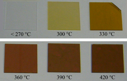
Fig. 11. Photographic image of the solution-processed films coated on quartz substrate. The films were pyrolyzed at Tp = 270–420 °C. The substrate size is 2 × 2 cm2. Reproduced with permission from Ref. 27. Copyright © 2012, Elsevier B.V.
Download figure:
Standard image High-resolution imageTo study the pyrolysis directly, TG and DTA measurements of poly(dihydrosilane) were conducted. Figure 12 shows the TG signal (bold solid line) and the DTA signal (thin solid line) as a function of heating temperature Th. Also shown is the temperature/time derivative DTG (dashed line) of the TG signal. The TG data indicate a weight loss of about 58% with heating up to 360 °C, and consequently only 42% of the material remains in the form of hydrogenated amorphous silicon. In agreement with thermal desorption spectroscopy (TDS) measurements.1) One may assume that the weight reduction is caused by the desorption of H2 and SiHx. According to the DTG curves, major weight losses take place at Th = 100, 200, and 300 °C. A broad exothermal peak is found in the DTA signal extending from 80 to 450 °C with a maximum near 320 °C. These results suggest that the transformation from a polymer to a cross-linked amorphous silicon network (i.e., Si–Si bond construction) is particularly active between 300 and 360 °C.
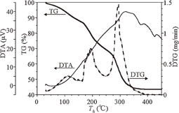
Fig. 12. TG (bold solid line), DTA (thin solid line), and DTG (dashed line) curves for poly(dihydrosilane) as a function of heating temperature. Reproduced with permission from Ref. 27. Copyright © 2012 Elsevier B.V.
Download figure:
Standard image High-resolution image4.2. Raman scattering analysis
Figures 13(a) and 13(b) show the first-order Raman spectra of the films prepared at Tp in the range of 270–330 and 330–420 °C, respectively. The Raman data were averaged over 10 measurements for each sample in a backscattering geometry using a He–Ne laser line (633 nm). In Fig. 13(a), typical phonon bands of a-Si:H28,29) are visible at Tp = 330 °C, however, the films prepared at Tp = 270 and 300 °C show no clear peaks corresponding to the amorphous silicon phonon bands. In the literature, the a-Si:H Raman phonon bands at 476, 387, 288, and 154 cm−1 have been assigned to the transverse optical (TO), longitudinal optical, longitudinal acoustic, and transverse acoustic bands, respectively. Figure 13(b) shows the Raman spectra of the films prepared at Tp = 330, 360, 390, and 420 °C, where the intensity was normalized to the same TO height. The full width at half maximum (FWHM) of the TO band vs Tp is plotted in Fig. 13(c).
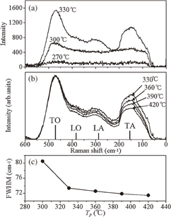
Fig. 13. (a) Raman spectra of the solution-processed films prepared at Tp = 270, 300, and 330 °C. (b) Raman spectra of the films prepared at Tp = 330, 360, 390, and 420 °C. The intensity was normalized to the same TO height. (c) FWHM of the TO Raman band vs Tp. Reproduced with permission from Ref. 27. Copyright © 2012 Elsevier B.V.
Download figure:
Standard image High-resolution image4.3. FT-IR and SIMS analyses
Figures 14(a) and 14(b) show the IR absorption coefficient α(ω) in the wavenumber ranges of 1950–2200 and 550–750 cm−1, respectively, for the annealed films prepared at Tp = 270–420 °C. The absorption peaks near 2000 and 2070–2090 cm−1 at Tp ≥ 360 °C are assigned to the stretching modes of Si–H bonds embedded in the bulk material and to the stretching modes of Si–H/Si–H2 bonds at the void surface, respectively.30) The absorption band near 640 cm−1 in Fig. 14(b) is attributed to the Si–H wagging mode.32) Only that of the sample prepared at 270 °C deviates significantly from this value. As seen in Fig. 14(a), the Si–H stretching modes of all the samples are centered near 2080 cm−1, except for the samples prepared at the rather low temperatures of 270 and 300 °C, which shifted to a higher wavenumber. We evaluated the sample quality using the infrared microstructure factor R expressed as

where I2090 and I2000 are the integrated intensities of the oscillation modes near 2070–2090 and 2000 cm−1, respectively. From the spectral data in Fig. 14(a), the estimated R ranges from 0.91 (Tp = 360 °C) to 0.80 (Tp = 420 °C), however, it is known that device-grade a-Si:H films show R < 0.230,31) because of the domination of the 2000 cm−1 peak. The large values of R for our films imply a void-rich structure. Although the origin of the peak shift at Tp ≤ 330 °C is not yet clear, it may be related to the oxidization or the change in the local environment of the Si–H dipole.33,34) This suggests that the films prepared at Tp ≤ 330 °C are of low quality.

Fig. 14. FT-IR absorbance spectra at (a) 1950–2200 cm−1 and (b) 550–750 cm−1 for the solution-processed films prepared at Tp = 270–420 °C on single-crystalline Si substrates. Reproduced with permission from Ref. 27. Copyright © 2012 Elsevier B.V.
Download figure:
Standard image High-resolution imageThe degrees of hydrogenation and oxidation were determined by FT-IR and SIMS. Figure 15 shows the hydrogen and oxygen contents as a function of Tp. The open circles show NH/NSi determined by FT-IR, in which the density of silicon is assumed to be NSi = 5 × 1022 cm−3. The density of hydrogen, NH, is evaluated from α(ω) in Fig. 14(b) using Eq. (7) with the proportional constant A640 = 2.1 × 1019 cm−2,35)

Since the hydrogen content of poly(dihydrosilane) is 67 at. %, the hydrogen concentrations of 9.2–10.6 at. % (by SIMS) of films prepared at Tp ≥ 360 °C indicate a remarkable reduction in the hydrogen content during the pyrolysis. The void-rich structure concluded from the large R value of films prepared at Tp ≥ 360 °C is presumably due to the 3D shrinkage due to the weight loss. The high oxygen content of the films prepared at Tp ≤ 330 °C indicates that the construction of the amorphous silicon network is not dense enough, thus it oxidizes rather easily in air.

Fig. 15. Hydrogen and oxygen content vs Tp. The closed circles and squares give the hydrogen and oxygen concentrations, respectively, estimated from the SIMS measurements. The open circles give the hydrogen content estimated from the IR absorption data by analyzing the wagging mode near 640 cm−1. Reproduced with permission from Ref. 27. Copyright © 2012 Elsevier B.V.
Download figure:
Standard image High-resolution image4.4. Properties of amorphous films
Figure 16 shows the results of absorption measurements in the UV–vis range for the films prepared at Tp = 300 to 420 °C. The data are depicted in a Tauc plot36) as

where α is the optical absorption coefficient, E is the photon energy in eV, B is a constant, and Eg is the optical gap (called the "Tauc gap"). B is found to be 5.7 × 10⁵ and 7.7 × 10⁵ eV−1 cm−1 for Tp = 300 and 330 °C, respectively, and 6.7 × 10⁵ eV−1 cm−1 for Tp ≥ 360 °C. The Tp dependence of Eg in Fig. 16(b) can be understood by the dehydrogenation during pyrolysis, as shown in Fig. 14. For Tp exceeding 360 °C, the absorption is no longer dependent on the hydrogen content, and Eg = 1.64 eV is obtained. This is consistent with Eg = 1.5–1.6 eV observed in the vacuum deposited counterparts.37,38)
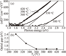
Fig. 16. (a) Tauc plot of the solution-processed films on a quartz substrate. The films were prepared at Tp = 300–420 °C. (b) Plot of Eg vs Tp. Reproduced with permission from Ref. 27. Copyright © 2012 Elsevier B.V.
Download figure:
Standard image High-resolution imageTypical values of the dark conductivity (σd), photoconductivity (σp), and spin density (Ns) at room temperature are plotted in Fig. 17 as a function of Tp. With increasing Tp from 300 to 330 °C, σd increases slightly, followed by a marked decrease at Tp = 360 °C, and reaches 5.1 × 10⁻¹¹ S/cm at Tp = 420 °C, while σp is on the order of 10−7 S/cm, except for the minimum at Tp = 360 °C. Ns, starting from 2.5 × 1016 cm−3 at Tp = 300 °C, exhibits a maximum in the film prepared at Tp = 360 °C, and reaches 2.8 × 1017 cm−3 for the high-Tp films. Since the paramagnetic spin density corresponds to the number of dangling bonds, which act as trapping sites, the reduction in Ns may lead to an increase in σp.39) The increase in Ns in the range from Tp = 300 to 360 °C is attributed mainly to the increase in the number of dangling bonds due to the breaking of the Si–H and Si–Si bonds. In contrast, the decrease in Ns in the range from Tp = 360 to 420 °C suggests that the high Tp has an annealing effect to reduce the number of dangling bonds [see also the FWHM data in Fig. 13(c)]. The photosensitivity (i.e., ratio of σp to σd) of the films prepared at Tp ≥ 360 °C is on the order of 103, whereas that of device-grade vacuum-processed a-Si:H films is 105–106.37,40) This low photosensitivity indicates the rather poor quality of the solution-processed films, which is presumably related to the high Ns > 1017 cm−3 for Tp ≥ 360 °C. Note that device-grade vacuum-processed a-Si:H films generally have Ns ≤ 1016 cm−3.37)
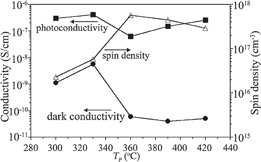
Fig. 17. Conductivity and spin density of the solution-processed films prepared at Tp = 300–420 °C. The values of σd and σp at room temperature and of NS are depicted by closed circles, closed squares, and open triangles, respectively. Reproduced with permission from Ref. 27. Copyright © 2012 Elsevier B.V.
Download figure:
Standard image High-resolution image5. Fabrication of devices from Si ink
Thus far, the devices we have developed using liquid Si are polycrystalline Si-TFTs,1) single-grained Si-TFTs,41,42) and thin-film solar cells.43) In TFTs fabrication, the excimer laser crystallization technique was adopted to convert an amorphous film to a polycrystalline one in a polycrystalline Si-TFT, or to convert CPS directly to a single-crystal grain using a grain filter in a single-grained Si-TFTs. These TFTs exhibited excellent properties, competitive with their conventional counterparts, demonstrating that the semiconductor films used in them are of high quality once converted to a crystalline form via melting. All defects formed in solid films during pyrolysis can be reset through melting. In amorphous films, however, the film quality is totally dependent on the pyrolysis process. This means that it is far more difficult to obtain device-grade amorphous films than fabricating device-grade crystalline films. That is, research on amorphous films for use in semiconductor applications is quite challenging. Here, we describe our attempt to develop a solar cell using amorphous films from Si ink. Figure 18 shows a schematic structure of the hydrogenated amorphous Si (a-Si:H) p–i–n single-junction solar cell that we developed.

Fig. 18. Schematic of a solution-processed a-Si:H solar cell structure.
Download figure:
Standard image High-resolution image5.1. Formation of doped films
For the fabrication of the p–i–n junction structure, we prepared doped and non-doped a-Si:H films. For the p-type a-Si:H (p-Si) film, p-type poly(dihydrosilane) was synthesised by the photoinduced ring-opening polymerization of CPS, in which decaborane was dissolved at 80 °C. The dopant concentration of the film was adjusted by changing the quantity of decaborane in the CPS. The wavelength, intensity, and irradiation time for the UV-light-induced reaction were 365 nm, 15 mW/cm2, and 10–60 min, respectively. The resultant polymer was dissolved in distilled CPS as the solvent. This p-type silicon ink [poly(dihydrosilane) solution] was spin-coated on a substrate and pyrolyzed at Tp = 390 °C for 30 min in a sealed chamber to prevent the desorption of decaborane. For the n-type a-Si:H (n-Si) film, n-type silicon ink was prepared using white phosphorus as the dopant.44) The wavelength, intensity, and irradiation time were 405 nm, 300 mW/cm2, and 5–120 min, respectively. Distilled cyclooctane was used as the solvent for the n-type silicon ink. The ink was spin-coated on the substrate and pyrolyzed at Tp = 390 °C for 30 min on a hot plate. For the intrinsic a-Si:H (i-Si) film, nondoped silicon ink was also prepared using distilled cyclooctane as a solvent. The wavelength, intensity, and irradiation time were 365 nm, 15 mW/cm2, and 10 min, respectively. The i-Si film was fabricated similarly to the n-Si film.
These p- and n-Si doped films were confirmed to be in the amorphous state from the Raman spectrum of phonon bands. The σd at 25 °C for the p- and n-Si films with a thickness of 50 nm are plotted as a function of boron or phosphorus concentration in Fig. 19. The dopant concentration was measured by SIMS. The σd values of both the p- and n-Si films show a significant increase with dopant concentration. These results suggest that boron and phosphorus in the doped a-Si:H films act as the acceptor and donor, respectively. The conductivity of our solution-processed doped a-Si:H films is one to three orders of magnitude smaller than that of device-grade vacuum-processed a-Si:H films.45) The maximum concentrations of boron and phosphorus are limited by the solubility of decaborane and white phosphorus in CPS, which are 7 × 10²¹ and 2 × 1021 cm−3, respectively.
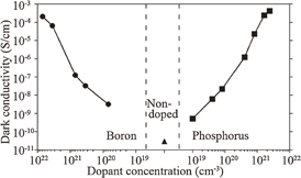
Fig. 19. σd vs dopant concentration for the p- and n-Si films at 25 °C. σd for the i-Si film is also plotted. σd values of the p-, i-, and n-type films are plotted by closed circles, a triangle, and squares, respectively. Reproduced with permission from Ref. 43. Copyright © 2012 American Institute of Physics.
Download figure:
Standard image High-resolution image5.2. Improvement film quality by hydrogen-radical treatment
The film quality was found to be improved by hydrogen-radical treatment via hot-wire chemical vapor deposition. The apparatus used was nearly identical to that described in the literature.46) A tungsten wire with a diameter of 0.5 mm and a length of 100 cm was used as the catalyst and was heated at 1850 °C. Hydrogen gas (99.9999% purity) was introduced into the chamber at a flow rate of 15 sccm for 15 min. The chamber pressure and substrate temperature were maintained at 0.2 Pa and 200 °C, respectively. The properties of the i-, p-, and n-Si films with and without the hydrogen-radical treatment are listed in Table III. Typical properties of the vacuum-processed i-Si films are also listed for reference. An increase in hydrogen content and a marked reduction in spin density by the hydrogen-radical treatment were observed in all of the silicon films. The depth profile obtained by SIMS measurement showed that the hydrogen contents increased not only on the surface but also entire film. This indicates that hydrogen radicals diffused in the film and terminated the defects. As a result, with this treatment, a large increase in σp and a decrease in σd in the i-Si film were achieved, and the σd values of the p- and n-Si films were increased. These properties of the resultant a-Si:H films were comparable to those of device-grade vacuum-processed ones.37) These improvements may be attributed to the reduction in spin density.
Table III. Properties of i-, p-, and n-Si films with and without the hydrogen-radical treatment.
| Hydrogen-radical treatment | i-Si | p-Sia) | n-Sib) | i-Si (ref)c) | |||
|---|---|---|---|---|---|---|---|
| with | without | with | without | with | without | without | |
| Hydrogen content (at. %) | 9.9 | 9.8 | 10.5 | 10.0 | 12.0 | 9.7 | 10 |
| Optical gap (eV) | 1.64 | 1.64 | 1.67 | 1.66 | 1.67 | 1.67 | 1.72 |
| Spin density (cm−3) | <2 × 10¹⁶ | 5 × 10¹⁷ | 1 × 10¹⁷ | 6 × 10¹⁷ | 6 × 10¹⁶ | 4 × 10¹⁷ | <2 × 10¹⁶ |
| Photoconductivityd) (S/cm) | 0.9 × 10⁻⁵ | 1.5 × 10⁻⁷ | — | — | — | — | 1.6 × 10⁻⁵ |
| Dark conductivity (S/cm) | 2.0 × 10⁻¹¹ | 4.0 × 10⁻¹¹ | 5.0 × 10⁻⁴ | 2.1 × 10⁻⁴ | 5.6 × 10⁻³ | 4.3 × 10⁻⁴ | 2.0 × 10⁻¹¹ |
a) The boron concentration is 7 × 1021 cm−3. b) The phosphorus concentration is 2 × 1021 cm−3. c) Prepared by plasma-enhanced chemical vapour deposition. d) An AM-1.5G solar simulator with an intensity of 100 mW/cm2 was employed.
Hydrogen-radical treatment reduced the spin density of the silicon films, while the use of heat treatment at temperatures of 100–400 °C in a hydrogen atmosphere had little effect on defect reduction in the films. We clarified that hydrogenation using hydrogen radicals is effective for the improvement in film quality.
5.3. Fabrication of solar cell
The solar cell shown in Fig. 18 was fabricated by the following four steps: (1) a flat ZnO layer with a sheet resistivity of 100 Ω/sq and a thickness of 200 nm was sputtered onto a glass substrate with an area of 5 × 5 cm2, (2) a p-Si layer (thickness: 30 nm) was fabricated on the ZnO substrate followed by the stacking of i-Si (thickness: 120 or 400 nm) and n-Si layers (thickness: 30 nm), (3) hydrogen-radical treatment was performed after fabricating the p–i–n structure, and (4) a 200-nm-thick Al electrode with an area of 5 × 5 mm2 was deposited on the p–i–n structure by vacuum evaporation.
Three types of solar cell (cells 1, 2, and 3) were fabricated by changing the thickness of the i-Si layer and the dopant concentration of the p-Si layer, as listed in Table IV. Figure 20 shows the depth profiles for boron, phosphorus, zinc, carbon, oxygen, and nitrogen for cell 1. It can be observed that boron and phosphorus diffused in the i-Si layer, and that the concentration of these elements in the i-Si layer fell below the detection limit within 20–40 nm from each interface. We also confirmed that boron diffuses extensively into the i-Si layer at Tp >390 °C (data not shown). Therefore, the upper limit of the fabrication temperature for a p–i–n structure with a satisfactory interface is 390 °C. Figure 20(b) shows that carbon, oxygen, and nitrogen are distributed in the p–i–n structure at a concentration of 1019–1021 cm−3, which increases at each interface.
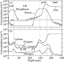
Fig. 20. Depth profiles of impurities for cell 1 measured by SIMS. (a) Boron, phosphorus, and zinc. (b) Carbon, oxygen, and nitrogen. Tp = 390 °C. Reproduced with permission from Ref. 43. Copyright © 2012 American Institute of Physics.
Download figure:
Standard image High-resolution imageTable IV. Thickness (in nm) and dopant concentrations (in cm−3) of the p-, i-, and n-Si layers in cells 1, 2, and 3.
| Cell 1 | Cell 2 | Cell 3 | |
|---|---|---|---|
| n-Si: thickness | 30 | 30 | 30 |
| (concentration) | (2 × 10²¹) | (2 × 10²¹) | (2 × 10²¹) |
| i-Si: thickness | 120 | 120 | 400 |
| p-Si: thickness | 30 | 30 | 30 |
| (concentration) | (7 × 10²¹) | (1 × 10²¹) | (7 × 10²⁰) |
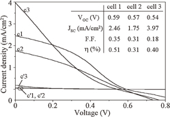
Figure 21 shows the current density–voltage (J–V) characteristics at 25 °C of the solution-processed solar cells with and without the hydrogen-radical treatment. The J–V curves denoted by c1, c2, and c3 and c'1, c'2, and c'3 correspond to cells with and without the hydrogen-radical treatment, respectively. Moreover, photovoltaic parameters such as the open-circuit voltage (Voc), short-circuit current (Jsc), fill factor (FF), and energy conversion efficiency (η) of the cells are shown in the figure. It is found that the hydrogen-radical treatment significantly improved Jsc from <0.2 to >1.7 mA/cm2. Accordingly, η was improved from <0.01 to >0.30% for all cells. This enhancement in Jsc by the hydrogen-radical treatment may be due to the large improvement in photoconductivity for the i-Si layer, as shown in Table III.
Fig. 21. J–V characteristics of the solar cells with a top electrode size of 5 × 5 mm2. The curves denoted by c1, c2, and c3 (c'1, c'2, and c'3) represent the J–V curves for cells 1, 2, and 3 with (without) the hydrogen-radical treatment, respectively. The inset shows the photovoltaic parameters and energy conversion efficiencies for cells 1, 2, and 3 with the hydrogen-radical treatment. The curves were measured using a solar simulator under the illumination condition of AM-1.5G (100 mW/cm2). Reproduced with permission from Ref. 43. Copyright © 2012 American Institute of Physics.
Download figure:
Standard image High-resolution image
Cell 3 shows the highest Jsc among all the cells and is characterized by a low Voc, it also has the lowest FF among the cells. The highest Jsc of cell 3 originated from the thicker i-Si layer of this cell than those of cells 1 and 2. The lowest FF value might have been related to the film quality of the i-Si layer. Observation of micrographs revealed that cell 3 had a few cracks, which is associated with pyrolysis of the thick (400 nm) i-Si layer. These defects may become a leakage current path and result in the degradation of the insulation of the cell.
In conclusion, solar cells with an a-Si:H p–i–n structure were successfully fabricated using doped and nondoped poly(dihydrosilane) solutions. We have demonstrated the effectiveness of hydrogen-radical treatment for improving the conductivity of a-Si:H layers by the reduction in spin density. The solution-processed a-Si:H solar cells were shown to have η of 0.31–0.51% under AM-1.5G (100 mW/cm2) illumination.
6. Summary
To enable the use of a solution process, we have been developing liquid Si using CPS which belongs to the hydrosilane group. CPS can be converted to poly(dihydrosilane) by a ring-opening reaction using UV light. The synthesized poly(dihydrosilane) is dissolved to make Si ink. Si ink is coated on a substrate to form a polymer film which in turn is pyrolyzed to a solid amorphous film. Crystal forms are also obtained by the excimer laser annealing of the amorphous Si film. Thus far, we have developed polycrystalline Si-TFTs, single-grained Si-TFTs, and thin-film solar cells.
In this review article, we introduced a series of our studies of liquid Si. The first topic was about CPS itself. We clarified its structure and physical properties by computer calculation and experiments. The most stable structure of CPS is the twist (C2) structure which is distorted compared with its hydrocarbon counterpart (cyclopentane). CPS is a transparent liquid between −10 and 194 °C. We investigated the polymerization process of CPS by constructing a SEC-MALLS-viscometry system. CPS can be polymerized swiftly by the irradiation of UV light of 365 nm wavelength. However, CPS just after distillation does not absorb 365 nm light and tends to be thermally polymerized even at room temperature. Therefore, we supposed that the energy of light once absorbed by the thermally-induced polymers is then transferred to CPS molecules to induce their polymerization. By using the data measured using the SEC-MALLS system, we deduced the scaling relation [η] = 0.414Mα, where α was found to be 0.206. This suggests that poly(dihydrosilane) has a spherelike structure having branched chains in solution. Si ink is coated on a substrate to make a polymer film. This process is not simple; in some cases, the polymer film ruptures to form many dots when the solvent dries. Whether or not a good film is formed or not depends on the interaction between polymer units and the substrate is intermediated by the solvent. When the interaction is attractive, a homogeneous film tends to be formed; when it is repulsive, dots tends to form. We clarified the criteria of film formation by calculating the Hamaker constant using optical parameters. The pyrolysis of polymers takes place mostly at temperatures of approximately 300 °C, where a polymer Si film can be converted to an amorphous Si film by resulting in a color change from transparent to yellow-brown. The color change indicates that the film is converted from an insulator to a semiconductor. The optimized pyrolysis temperature ranged between 360 and 420 °C in terms of semiconductor properties. However, the photosensitivity of the films thus prepared was only on the order of 103. This is 2–3 orders of magnitude lower than that of device-grade a-Si:H films. This indicates that the poor quality of solution-processed films is related to the low film density generating a high spin density Ns > 1017 cm−3. Fortunately, however, the film quality can be improved by hydrogen-radical treatment: Ns was reduced to less than 2 × 10¹⁶ and photosensitivity was enhanced up to the order of 105. On the basis of these results, we tried to develop solar cells using a-Si:H films for the p–i–n structure. Both n- and p-type doped inks were synthesized, and doped films that satisfied the required specifications for solar cells were also developed using these inks. The solution-processed a-Si:H solar cells were shown to exhibit 0.31–0.51% efficiency under AM-1.5G (100 mW/cm2) illumination.
Acknowledgments
We thank Dr. Y. Matsuki for his major contribution to this research. We thank Professors T. Mitani, S. Katayama, and A. Sugiyama as well as Dam Hieu Chi for discussions and valuable comments about the structure and properties of both CPS and the polymer. We thank Mr. H. Takagishi and Dr. Z. Shen for their advice in our experiments. We also thank the researchers of Sanyo Corporation (now Panasonic) for collaborative work in developing solar cells. This study was funded by the Exploratory Research for Advanced Technology (ERATO) program of Japan Science and Technology Agency. The computational study was partly supported by the Special Coordination Funds for Promoting Science and Technology commissioned by the Ministry of Education, Culture, Sports, Science and Technology, Japan, by the Special Project QGTD.08.09 commissioned by the Vietnam National University, Hanoi, and by the Fundamental Research Project 103.02.111.09 commissioned by NAFOSTED, Vietnam. The computations presented in this study were performed at the Center for Information Science, Japan Advanced Institute of Science and Technology.