Abstract
This paper presents a systematic characterization of electronic states at insulators/(Al)GaN interfaces, particularly focusing on insulator/AlGaN/GaN structures. First, we review important results reported for GaN metal–insulator–semiconductor (MIS) structures. SiO2 is an attractive material for MIS transistor applications due to its large bandgap and high chemical stability. In-situ SiNx is effective for improving the operation stability of high electron mobility transistors (HEMTs). Meanwhile, Al2O3/GaN structures have high band offsets and low interface state densities, which are also desirable for insulated gate applications. We have proposed a calculation method for describing capacitance–voltage (C–V) characteristics of HEMT MIS structures for evaluating electronic state properties at the insulator/AlGaN interfaces. To evaluate near-midgap states at insulator/AlGaN interfaces, a photo-assisted C–V technique using photon energies less than the bandgap of GaN has been developed. Using the calculation in conjunction with the photo-assisted C–V technique, we estimate interface state density distributions at the Al2O3/AlGaN interfaces.
Export citation and abstract BibTeX RIS
1. Introduction
Advanced GaN-based device technologies have very recently attained a cutoff frequency of 450 GHz and a maximum oscillation frequency of 500 GHz.1) In addition, excellent power-switching performances with high-blocking voltages and low on-state resistances have been reported for AlGaN/GaN high electron mobility transistors (HEMTs).2–7) Continuous demand for improved device technology has made insulated-gate and surface-passivation structures inevitable for power switching transistors. In particular, the insulating gate dielectric plays an important role in blocking the leakage current when the gate is driven with a forward bias. Furthermore, the deposition of insulator films on the access region surface of the transistor controls surface traps, leading to operation stability and reliability improvement.
In this regard, different insulator materials have been applied to GaN-based transistors including HEMTs. Nonetheless, interface properties of insulator/(Al)GaN structures are still not fully understood. From the viewpoint of the HEMT application, it is desirable to evaluate interface state properties using an actual AlGaN/GaN structure with a very thin AlGaN layer (15–25 nm). However, in comparison with a conventional metal–insulator–semiconductor (MIS) structure having a single semiconductor layer, it is difficult to characterize the insulator/AlGaN interfaces in MIS HEMTs. MIS HEMTs have two interfaces: insulator/AlGaN and AlGaN/GaN, making the potential modulation rather complicated. In addition, the emission efficiency of electrons from the wide-gap interface states to the conduction band is very limited at room temperature (RT).
Although there have been many reports of low interface-trap densities in HEMT MIS capacitors, several papers have incorrectly evaluated their capacitance–voltage (C–V) characteristics, underestimating the actual interface state density for wide-bandgap semiconductors. When the gate voltage sweeping is confined within the reverse bias region, the resulting C–V curve often gives rise to misleadingly low density of electronic states at the insulator/AlGaN interfaces.8,9) A HEMT MIS structure typically shows a two-step C–V behavior.10) However, several groups reported C–V curves without the characteristic step at the forward bias regime.11,12) In this case, it is likely that high-density states at the insulator/AlGaN interface impede the potential control of the AlGaN surface by the gate bias. In addition, the present GaN-based MIS HEMTs are suffering from threshold voltage fluctuations,13–15) probably due to different charging states of interface traps under different operating conditions. To aid the advancement of insulated gate and surface passivation technologies, suitable characterization methods are needed for understanding the effects of interface states on the C–V behavior of the HEMT MIS structures. A combination of recessed and insulated gates is often used in normally-off AlGaN/GaN HEMTs. Since the interface quality greatly affects the transistor performance, evaluating interface properties of HEMT MIS structures fabricated on the dry-etched AlGaN surfaces is suitably important.
Accordingly, this paper presents characterization of electronic states at insulators/(Al)GaN interfaces, particularly focusing on insulator/AlGaN/GaN structures. First, we review important results reported for GaN-based MIS structures. We have developed a numerical calculation method for obtaining C–V characteristics of HEMT MIS structures. Using this method, we then present the effects of electronic states at the insulator/AlGaN interface on the C–V behavior of HEMT MIS capacitors. To evaluate near-midgap interface states at RT, we have proposed a photo-assisted C–V characterization technique using photon energies less than the bandgap of GaN. On the basis of the calculation and the photo-assisted C–V analysis, we estimate interface state density distributions at the Al2O3/AlGaN interfaces with and without dry etching of the AlGaN surface.
2. Band lineups between GaN and relevant insulator materials
For a structure design of an MIS transistor or a surface-passivated transistor using a wide-gap semiconductor, it is important to understand the band lineup between the insulator and the semiconductor involved. Figure 1 shows the plot of energy gap versus dielectric constant for relevant insulators and nitride compounds. It is a common knowledge that a higher value of dielectric constant leads to a higher value of transconductance gm. From this point of view, SiO2 is at a disadvantage compared with the other dielectric materials. Also, a large band-offset energy is required at the insulator/AlGaN interface for the suppression of leakage current. On this account, MIS gate structures employing Si3N4, ZrO2, and HfO2 dielectric materials are relatively susceptible to leakage current problems. On the other hand, Al2O3 is one of the most attractive dielectric materials for power MIS devices because it combines all the desired properties such as large bandgap, relatively high dielectric constant, and high breakdown field (∼10 MV/cm).
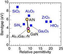
Fig. 1. Energy gap EG versus dielectric constant ε for various insulators and GaN compounds.
Download figure:
Standard image High-resolution imageFigure 2 shows the band lineups between GaN and several insulators reported by Robertson and Falabretti.16) They calculated charge neutrality levels (ECNL) for GaN and insulators and determined the lineup using ECNL as the reference energy level. All interfaces result in the type-I alignment. Note that the bandgap of Al2O3 used in the calculation is that of the bulk, which is higher than those values (6.7–7.0 eV) obtained experimentally from amorphous films.17–19) Calculations predict that Ga2O3, SiNx and HfO2 interfaces produce relatively low barriers at the conduction band ΔEC. Similar values were obtained from X-ray photoelectron spectroscopy analyses and leakage current characterizations.20–25) Relatively high leakage current may arise at forward bias when these insulators are used in the insulated gate structures. On the other hand, the resulting ΔEC values from Al2O3 and SiO2 are high enough for gate applications.17,26–28)
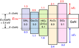
Fig. 2. Band lineups at insulators/GaN interfaces calculated by Robertson and Falabretti.16) The charge neutrality level, ECNL, acts as the reference energy level for the lineup. Note that the bandgap of Al2O3 used in the calculation is that of the bulk, which is higher than that of an amorphous film reported experimentally.
Download figure:
Standard image High-resolution image3. Interface properties of GaN MIS structures
3.1. SiO2/GaN structure
Gaffey et al.26) reported a precise characterization of interface properties of a SiO2/SiNx/SiO2/n-GaN structure prepared by jet vapor deposition. From the conductance–frequency analysis, they obtained a state density of 5 × 1010 cm−2 eV−1 at EC − 0.8 eV with a capture cross section of 2.4 × 10⁻¹⁷ cm2 for the MIS sample fabricated using the optimum process condition. Matocha et al.29) and Kim et al.30) presented low state densities at the SiO2/n-GaN interfaces prepared at high temperatures (830–900 °C). Kanechika et al.31) fabricated a vertical-type AlGaN/GaN MOS HEMT, demonstrating good I–V characteristics with a high on/off ratio using a SiO2 film thermally deposited at 830 °C. It was also found that high-temperature annealing process after the SiO2 deposition was also effective in decreasing the interface state density.32–35) Kambayashi et al.34) reported over 100 A operation in AlGaN/GaN hybrid HEMT using the SiO2 gate dielectric post-deposition annealed at 700 °C. Very recently, a channel mobility of 192 cm2 V−1 s−1 was achieved in a hybrid HEMT using a Al2O3/SiO2 bilayer gate structure.36) Although the SiO2 film has a low permittivity as shown in Fig. 1, it remains attractive for MIS HEMT applications because of its large bandgap and chemical stability.
3.2. SiNx/GaN structure
The SiNx film is widely used for surface passivation of GaN-based transistors. Hashizume et al.20,37) demonstrated that the SiNx deposition on N2-plasma treated surfaces can produce a good SiNx/n-GaN interface with a state density as low as 1 × 1011 cm−2 eV−1 at EC − 0.8 eV. The reason for the low interface state densities at the SiNx/n-GaN interface is not yet fully understood. It is likely that nitrogen radicals generated during the SiNx deposition process control the formation of nitrogen-vacancy-related defects at the GaN surface,38) leading to the prevention of interface electronic states. Green et al.39) were the first to apply-SiNx passivation to the AlGaN/GaN HEMTs, and have observed a significant improvement of microwave output power as a consequence.
The in-situ deposition of SiNx is an interesting process in the sense that it can be performed in the same growth chamber and in the same growth sequence as the rest of the layer stack.40) During the final growth stage of the AlGaN/GaN structure by metal organic chemical vapor deposition, the SiNx layer was in-situ deposited using NH3 and SiH4 on the AlGaN surface at 1020 °C. Derluyn et al.40) obtained improved I–V characteristics from HEMTs with the in-situ deposited SiNx layer. The in-situ process realized an oxide-free SiNx/AlGaN interface.41) From the high-resolution transmission electron microscopy (HR-TEM) analysis, Takizawa et al.42) reported that the in-situ SiNx has a single crystalline structure. Very recently, Van Hove et al.3) demonstrated that an AlGaN/GaN HEMT with a stable threshold voltage and a low current collapse can be achieved using an in-situ SiNx/Al2O3 bilayer gate.
3.3. Al2O3/GaN structure
As mentioned in Sect. 2, the Al2O3 has a large bandgap, a relatively high dielectric constant and a high breakdown field. In addition, there has been considerable progress of atomic layer deposition (ALD) technology, simplifying the application of Al2O3 to the gate and passivation structures in the GaN transistors.43–45) Park et al.46) were the first to report AlGaN/GaN MOS HEMTs using an Al2O3 prepared by ALD as a gate dielectric and a surface passivation layer. The ALD process realized good Al2O3/n-GaN interface with a low state density of around 1 × 1011 cm−2 eV−1 at EC − 0.8 eV.17,47)
When using Al2O3, special attention should be given to subsequent process temperatures. From the transmission electron microscope (TEM) observation, Hori et al.17) found a flat and smooth atomic arrangement around the ALD prepared amorphous Al2O3/n-GaN interface. However, annealing at 800 °C for the formation of ohmic electrodes generated a large number of microcrystallized regions in the Al2O3 layer, causing a marked increase in the leakage current of the Al2O3/GaN structure. Toyoda et al.48) also reported that annealing procedures at 800 °C resulted in the phase transformation of Al2O3 films from amorphous to crystalline. To address this issue, an ohmic-first process, i.e., formation of ohmic electrodes including annealing at 800 °C before the Al2O3 deposition, was developed for Al2O3/n-GaN structures.17) This method effectively suppresses leakage current in MOS structures. Nevertheless, even in this scheme, a surface protection layer is indispensable to avoid the chemical bond disorder at the GaN surface during the annealing process. Optimization of the ohmic-first process using a SiNx surface protection layer then realized a good Al2O3/n-GaN interface with a low state density of 2 × 1011 cm−2 eV−1 at EC − 0.8 eV.17)
For practical applications of Al2O3 to the MOS HEMTs, stability and reliability characterization of the Al2O3 films is necessary. From a time-dependent dielectric breakdown measurement, Kikuta et al.49) reported that a time-to-breakdown (tBD) at 3 MV/cm for the ALD-Al2O3 film was more than 40000 years at RT. However, the tBD significantly decreased to 102–103 s at 250 °C. Esposto et al.28) and Son et al.50) pointed out that relatively high densities of fixed charges in Al2O3 films shifted flat-band voltages in the C–V curves of the Al2O3/n-GaN capacitors. The origin for the fixed charges is not clear yet. Choi et al.51) theoretically predicted that the oxygen vacancy in Al2O3 introduces transition levels close to the conduction band edge of GaN, and it can act as border traps at the Al2O3/n-GaN interface. On the other hand, it is likely that other kinds of defects such as Al vacancy and interstitials act as fixed charges in Al2O3.51)
3.4. High-κ insulators/GaN structure
High-κ insulators are attractive for the MIS transistors for achieving high gm. Recently, relatively good I–V characteristics were reported for AlGaN/GaN HEMTs with high-κ gate insulators.52–55) Hatano et al.55) demonstrated the improved operation stability in the AlGaN/GaN HEMT with an Al2O3/ZrO2 bilayer gate dielectric. However, interface properties of high-κ/AlGaN structures are not well understood. In addition, severe Vth fluctuations were reported by Hayashi et al.56) and Stoklas et al.57) in HEMTs with HfO2- and ZrO2-gate dielectric materials, respectively. Therefore, further investigation is necessary to gain better understanding of high-κ insulators/(Al)GaN interfaces.
4. HEMT MIS structures
4.1. Interpretation of HEMT MIS C–V characteristics
To improve device performance and stability of MIS HEMTs using AlGaN/GaN and InAlN/GaN structures, evaluation of electronic state properties of the interfaces between insulators and AlGaN/InAlN is of utmost importance. However, fabrication of a simple MIS diode using a thick AlGaN or InAlN is challenging due to the difficulty of growing high-quality epitaxial layers. For the practical device application, it is desirable to characterize insulator/AlGaN or insulator/InAlN interfaces using HEMT MIS structures. In this regard, we initially attempt to interpret precisely the resulting C–V characteristics of the HEMT MIS structures.
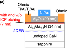
Figure 3(a) shows a schematic illustration of the HEMT MIS structure used in this study. An undoped AlGaN/GaN heterostructure grown on a sapphire substrate by metal organic chemical vapor deposition (MOCVD) was used as the starting wafer (provided by NTT-AT). The sheet resistance and mobility of the AlGaN/GaN heterostructure were 500 Ω/sq. and 1750 cm2 V−1 s−1, respectively. We prepared Al2O3/AlGaN/GaN samples with and without dry etching of the AlGaN surface. For the etching of AlGaN, we used a Cl2-based dry etching process assisted by inductively coupled plasma (ICP) at RT. The ICP and bias powers were 300 and 5 W, respectively. The resulting etching depth was 7 nm. We then deposited a 10-nm-thick SiNx film as a surface protection layer to avoid damage to the AlGaN surface during ohmic annealing.17) As an ohmic electrode, a ring-shaped Ti/Al/Ti/Au multilayer structure was deposited on the AlGaN surface, followed by annealing at 800 °C for 1 min in N2 ambient. After removing the SiNx film, an Al2O3 layer with a nominal thickness of 20 nm was deposited at a deposition rate of 0.11 nm/cycle on the AlGaN surface using an ALD system (SUGA-SAL1500) at 350 °C for 170 cycles. During the deposition process, water vapor and TMA were introduced into an ALD reactor in alternate pulse forms. Finally, a circular Ni/Au (20/50 nm) gate electrode concentric with the ohmic electrode was deposited on the Al2O3 layer.
Download figure:
Standard image High-resolution image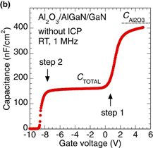
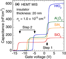
Fig. 3. (a) Schematic illustration of the Al2O3/AlGaN/GaN structure and (b) RT C–V curve of the HEMT MOS sample without ICP etching of AlGaN.
Download figure:
Standard image High-resolution imageFigure 3(b) shows a typical C–V curve of the Al2O3/AlGaN/GaN structure without the etching of the AlGaN surface. C–V measurements were carried out using an impedance analyzer (HP4192 LF) with a measurement frequency of 1 MHz at RT. A characteristic C–V curve with two steps was observed, which is peculiar to the MIS structure fabricated on the heterostructure including a two-dimensional electron gas (2DEG).10,44,58,59) The constant capacitance at the forward bias corresponds to the Al2O3 capacitance, whereas that at the reverse bias is determined by the total capacitance (CTOTAL) of the Al2O3 and AlGaN layers. At a deep reverse bias, the capacitance steeply decreases to nearly zero, indicating the 2DEG depletion at the AlGaN/GaN interface.
To understand this peculiar C–V behavior, we carried out calculations using a numerical solver of the Poisson equation based on the one-dimensional Gummel algorithm, taking into account the fixed charge at the AlGaN/GaN interface originating from spontaneous and piezoelectric polarization as well as the charge in the electronic states at the insulator/AlGaN interface.60) We assumed the 2DEG density of 1 × 1013 cm−2 and an insulator thickness of 20 nm. Other parameters used in calculation are listed in Table I, where ΦB is the Schottky barrier height at the metal/insulator interface, ΔEC1 and ΔEC2 are the conduction-band offsets between insulator/AlGaN and AlGaN/GaN interfaces, respectively. Figure 4(a) shows the calculated MIS C–V curves neglecting interface state density (ideal curve) for various insulators. The two-step behavior is reproduced in all HEMT MIS structures. Insulator capacitance, total capacitance (CTOTAL) and threshold voltage at the step 2 systematically change along with the changing value of permittivity as expected. The AlGaN-thickness dependence of the C–V curves is shown in Fig. 4(b). Similarly, a systematic change is seen in CTOTAL and the threshold voltage.
Download figure:
Standard image High-resolution image
Fig. 4. (a) The calculated C–V curves of HEMT MIS structures using some insulators without considering interface state density (ideal curve). (b) AlGaN-thickness dependence of C–V curves for the Al2O3/AlGaN/GaN structure.
Download figure:
Standard image High-resolution imageTable I. Parameters used in the calculations. ΦB is the Schottky barrier height at the metal/insulator interface. ΔEC1 and ΔEC2 are the conduction-band offsets between insulator/AlGaN and AlGaN/GaN interfaces, respectively (Ref. 16).
| SiO2 | SiNx | Al2O3 | HfO2 | |
|---|---|---|---|---|
| EG (eV) | 8.9 | 4.9 | 6.7 | 5.6 |
| εr | 3.9 | 7.0 | 9.0 | 15 |
| ΦB (eV) | 3.7 | 3.1 | 3.5 | 3.2 |
| ΔEC1 (eV) | 2.5 | 1.3 | 2.1 | 1.1 |
| ΔEC2 (eV) | 0.3 | 0.3 | 0.3 | 0.3 |
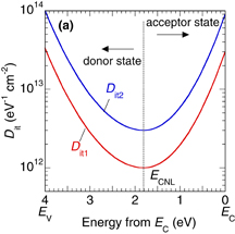
The ideal curves show almost the same slope at both steps 1 and 2. This is completely different from the experimental result shown in Fig. 3(b). To shed a light on this, we carried out calculations for the Al2O3/AlGaN/GaN structure, taking into account the effect of interface electronic states.60) Figure 5(a) shows the interface state density distributions Dit(E) used in calculation, illustrating the acceptor- and donor-like states divided by the charge neutrality level ECNL.60,61) We adapted the ECNL values calculated by Mönch in Ref. 62. In addition, we used electron emission time constant τ from interface states to the conduction band calculated using Shockley–Read–Hall (SRH) statistics:

where  TH, σTH, NC, and ET are electron thermal velocity, capture cross section, density of state at the conduction band, and interface state energy, respectively.
Download figure:
Standard image High-resolution image
Fig. 5. (a) Interface density distributions used in calculation and (b) the calculated C–V characteristics of the Al2O3/AlGaN/GaN structure with and without considering interface states.
Download figure:
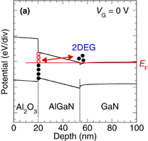
Standard image High-resolution imageThe calculated C–V curves are shown in Fig. 5(b). In the forward bias region, the C–V slope drastically decreases with increasing interface state density, similar to the experimental results. At forward bias, the nearly flat potential of the AlGaN layer shown in Fig. 6(a) can lead to the electron transfer with ease from the AlGaN/GaN interface to the Al2O3/AlGaN interface, resulting in the steep C–V slope relative to the case without interface states. However, in the actual case, electron trapping at the Al2O3/AlGaN interface states is highly probable. The acceptor-type states result in excess negative charges when they trap electrons. Such negatively charged interface states can screen the gate electric field, suppressing the potential modulation of the AlGaN layer. This causes the stretch out of the C–V curve, as shown in Fig. 5(b). In an extreme case, if a HEMT MIS sample includes very high interface state densities, then the step 1 will not be observed even at high forward bias. Indeed, several papers showed no C–V step even at high forward bias.11,12) On the other hand, in the reverse bias region, the stretch-out behavior was not observed in the C–V curve. Figure 6(b) shows the potential distribution at VG = −8 V. The Fermi level (EF) is located far below the valence band maximum of AlGaN at the Al2O3/AlGaN interface, which makes electron occupation of interface states no longer a function of the gate bias, leading to absence of stretch-out behavior in the C–V curve. In addition, Eq. (1) gives very long time constants of electron emission from deep states to conduction band. Therefore, electrons captured at deep states remain unaffected even when a large negative bias is applied to the gate electrode. This leads to the fact that the interface states act as "fixed and frozen" charges.
Download figure:
Standard image High-resolution image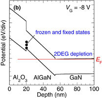
Fig. 6. Band diagrams of the Al2O3/AlGaN/GaN structure at (a) VG = 0 and (b) VG = −8 V.
Download figure:
Standard image High-resolution imageFigure 7 schematically shows the charge condition of the interface states at RT. When a value of 1 × 10⁻¹⁶ cm2 is used for the capture cross section of the interface states, only the upper half of the acceptor-like traps can change their charge state (NA0/NA−) accordingly with the gate voltage sweep. The acceptor-type states in this energy region produce excess negative charges when electrons are trapped, whereas they are in the neutral charge state when electrons are detrapped, mainly causing the stretch out of the C–V curve at the forward bias. Due to the associated long emission time constants, electrons in the lower half of acceptor-like traps remain trapped and act as negatively fixed charges, even when the EF is located far below the valence band maximum of AlGaN [Fig. 6(b)]. This leads to the parallel C–V shift (Vth shift) at step 2 toward the positive bias direction with respect to the ideal C–V curve, as shown in Fig. 5(b). The Vth shift is enhanced with increasing interface state density. Similarly, the donor-like traps remain on their neutral charge state (filled with electrons), independent of the bias sweeping. Since their neutral condition remains unchanged at RT, it is rather difficult to evaluate the effect of the donor-like traps by a standard C–V measurement.
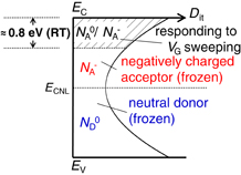
Fig. 7. Schematic illustration of charge condition of the interface states at RT. NA0 and ND0 indicate the neutral acceptor and donor states, respectively, and NA− denotes the negatively charged acceptor state.
Download figure:
Standard image High-resolution imageThe conductance method is often applied in HEMT MIS structures to analyze interface states.63–65) Using this technique, careful attention should be given to the EF position at the insulator/AlGaN interface. At reverse bias regime, the interface states could not be responsible for the conductance peak in the conductance–frequency (G–f) curve,63,64) because of the associated long emission time constants of interface states. In addition, Shih et al.65) pointed out that the conventional conductance method is viable only for a narrow range of gate bias voltages, and invalid for the analysis of deeper interface states. They proposed a unique characterization method using G–f characteristics at forward bias and high temperatures. From an analysis based on the G–f–T (temperature) mapping, they estimated an energy range of interface states responding to the G–f measurement and a gate control efficiency related to an interface state density.65)
4.2. Photo-assisted C–V analysis
To evaluate near-midgap electronic states at insulator/AlGaN interfaces at RT, we have developed a photo-assisted C–V method.10) Figure 8 shows schematic illustrations of photo-ionization effects of interface states under a monochromatic light with energy less than the bandgap of GaN. First, under dark condition, a forward gate voltage high enough to observe the insulator capacitance is applied. At this state, almost all of interface traps are filled with electrons under a nearly flat band condition. Then, the gate bias is swept toward a value more negative than the threshold voltage. After reaching a sufficiently negative gate bias, a monochromatic light with photon energy of hν1 is illuminated to the sample surface. Consequently, we are effectively inducing photo-assisted electron emission from the interface states within the energy range corresponding to the photon energy range, as schematically shown in Fig. 8(a). After switching the light off, we restarted the voltage sweep toward 0 V under dark condition. As shown Fig. 8(b), we can observe the C–V curve shift toward the reverse bias direction, corresponding to the change in the interface state charge Qit (hν1).
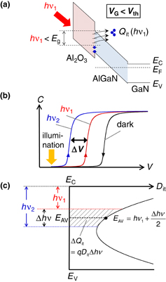
Fig. 8. Schematic illustration of (a) photo-assisted electron emission at the Al2O3/AlGaN interface, (b) photo-assisted C–V characteristics and (c) interface state charge and energy range corresponding to the voltage shift, ΔV, in photo-assisted C–V curves.
Download figure:
Standard image High-resolution imageUsing different photon energies, we can induce a systematic C–V shift according to the photon energy, as shown in Fig. 8(b). The voltage shift difference (ΔV) between two photon energies corresponds to the interface charge difference, ΔQit, in the energy range Δhν shown in Fig. 8(c). The state density can be simply estimated using the observed ΔV in the following equation:

where CTOTAL is the total capacitance of Al2O3 and AlGaN and EAV is the average interface energy schematically shown in Fig. 8(c).
It should be emphasized that the present method uses incident photons with energies less than the bandgap of GaN. On the other hand, some groups have reported photo-assisted C–V characterization of MIS structures using a light source with photon energies larger than the GaN bandgap.66,67) In this case, holes are generated and accumulated at insulator/AlGaN and AlGaN/GaN interfaces. In addition, interaction of holes with the interface states especially at reverse bias has to be considered. This makes the charge dynamics in HEMT MIS structures complicated and the evaluation of interface state states very difficult. Very recently, Matys et al.68,69) proposed a simulation method for the photo-assisted C–V characteristics, taking into account the electron–hole generation and the recombination processes as well as the hole capture process at the interface states. Comparing their calculation results to the experimental data, they were able to estimate the state density distribution at the Al2O3/AlGaN interface near the valence-band maximum of AlGaN.
4.3. Estimation of the state density distribution at Al2O3/AlGaN interface using HEMT MIS structures
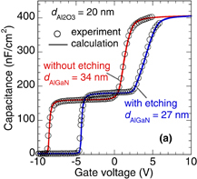
Using the combination of the numerical fitting of C–V curves and the photo-assisted C–V method, we have attempted to estimate the state density distribution of the Al2O3/AlGaN interfaces. Figure 9(a) shows the comparison between the calculated and experimental C–V curves of the Al2O3/AlGaN/GaN structure with and without the ICP dry etching of the AlGaN surface. As shown in Fig. 3(a), the initial HEMT structure has a 34-nm-thick AlGaN layer. After the ICP etching, the AlGaN thickness was reduced to 27 nm,70) causing an increase in CTOTAL and a pronounced Vth shift in the C–V curve. By assuming interface state density distributions indicated by the solid lines in Fig. 9(b), the calculation reasonably reproduced the experimental data. From the fitting results, we can determine the state density distribution near EC at the Al2O3/AlGaN interface. Note that it is difficult to evaluate the state density distribution at the energies above EC − 0.2 eV from C–V measurements at the frequency of 1 MHz, because electrons captured at such shallow interface states can respond to the measurement AC signal and accordingly give an inaccurate estimate of capacitance.
Download figure:
Standard image High-resolution image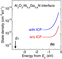
Fig. 9. (a) The comparison between the calculated and experimental C–V curves of the Al2O3/AlGaN/GaN structure with and without the ICP etching of AlGaN. By assuming interface state density distributions indicated by the solid lines in (b), the calculation reasonably reproduced the experimental data.
Download figure:
Standard image High-resolution imageFigure 10 shows the measured photo-assisted C–V curves of the sample with the ICP etching of AlGaN. We observed systematic C–V shifts toward the reverse bias direction with increasing photon energy, as explained in Sect. 4.2. The completely parallel C–V shift toward the negative direction indicates that the interface states near midgap or at deeper energies act as fixed charges in this bias range. Ozaki et al.71) recently reported a similar parallel C–V shift in an ALD-Al2O3/n-GaN/AlGaN/GaN structure. Using Eq. (2), we estimated the interface state densities in the samples with and without the ICP etching of AlGaN. Figure 11 shows the state density distributions at the Al2O3/AlGaN interface determined by the photo-assisted C–V and the fitting methods. The sample without the ICP etching of AlGaN showed state densities of around 1 × 1012 cm−2 eV−1 or less near the midgap. On the other hand, much higher state densities were obtained at the Al2O3/ICP-etched AlGaN interface.
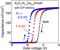
Fig. 10. Photo-assisted C–V characteristic of Al2O3/AlGaN/GaN structure with ICP etching of AlGaN.
Download figure:
Standard image High-resolution image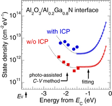
Fig. 11. State density distributions at the Al2O3/AlGaN interface determined by a combination of the photo-assisted C–V method and the C–V fitting analysis.
Download figure:
Standard image High-resolution image
From transmission electron microscopy (TEM) observations, it was found that the ICP etching process introduced a monolayer-level crystalline roughness to the AlGaN surface.70) As a result, lattice disorder and/or a high density of dangling bonds near step edges remained at the AlGaN surface, leading to the generation of high-density electronic states with a continuous energy distribution. During ICP etching using the Cl2/BCl gas mixture, active Cl-based radicals dominantly react with the AlGaN surfaces to form volatile products, such as GaCl3 and AlCl3. However, there are other possible chemical reactions. For instance, a highly volatile NCl3 can be formed by a reaction between the Cl-based radical and N atoms, causing a preferential loss of N atoms at the AlGaN surface.38) In fact, Fang et al.72) reported that several kinds of deep levels originating from defect complexes related to nitrogen vacancy were increased at the GaN surface after the Cl2-based ICP etching. It is thus likely that ICP etching causes the monolayer-level interface roughness, disorder of the chemical bonds and formation of various types of defect complexes at the AlGaN surface, leading to poor C–V characteristics due to high-density interface states at the Al2O3/AlGaN interface.
4.4. Vth fluctuation issue in MIS AlGaN/GaN HEMTs
Although various kinds of insulator materials have been applied to improve the performance of AlGaN/GaN HEMTs, several problems remain unsolved. Among the most serious issues is the Vth fluctuation. Several papers reported that different gate bias conditions cause the Vth shifts in MIS HEMTs.13–15) Fixed charges in insulator films,28,50) border traps51) and interface states at the insulators/AlGaN interfaces are involved in the Vth shift mechanism. As shown in Fig. 5(b), a higher interface state density leads to a shallower Vth. In addition, the charging state of the interface traps varies with the gate bias (EF position), as shown in Fig. 7, and the deeper states with long time constants for electron emission contribute to a slow Vth fluctuation.14) Lu et al.15) and Johnson et al.14) reported that the higher positive gate biasing of the MIS HEMTs induces larger Vth shift toward the forward bias direction. This is mainly related to the change in the density of ionized acceptor-type states, as shown in Fig. 7. Ťapajna and Kuzmík13) also pointed out the effect of interface states on the Vth shift in MIS HEMTs. To realize normally-off operation, a combination of a recessed and an insulated gate structure is often implemented in AlGaN/GaN HEMTs. However, dry etching process step for the formation of the recessed structure introduces some kinds of surface defects, resulting in high densities of electronic states at insulator/(Al)GaN interfaces, as shown in Fig. 11 and as reported in Refs. 47 and 70.
Yang et al.44) demonstrated that surface nitridation of GaN/AlGaN/GaN structure using remote N2 plasma is effective in improving a sub-threshold gate control and Vth stability of the Al2O3-gate HEMT. Hori et al.73) reported that N2O radical treatment can decrease interface states at the Al2O3/AlGaN interface, resulting in the improved stability of Vth even after applying an off-stress gate bias. Van Hove et al.3) utilized in-situ SiNx as an interfacial control layer, and reported improved operation stability with a small Vth fluctuation in the SiNx/Al2O3 gated AlGaN/GaN HEMT. On the basis of a systematic characterization of interface states, further investigation is absolutely necessary to control electronic states at insulator/(Al)GaN interfaces for improved stability of AlGaN/GaN MIS HEMTs.
5. Conclusions
It is inevitable to make use of insulator films for insulated-gate and surface-passivation structures in the GaN-based power switching transistors. In this regard, we have reviewed important reports on the characterization of interface properties of GaN MIS structures and operation characteristics of MIS AlGaN/GaN HEMTs. SiO2 is an attractive insulator material due to its favorable dielectric properties such as large bandgap and high chemical stability. A high-temperature deposition and/or a high-temperature annealing process can effectively reduce state density at the SiO2/GaN interface. SiNx is also an important passivation material for GaN-based transistors. In-situ deposition of SiNx during the MOCVD growth process can improve the operation stability of HEMTs. Meanwhile, Al2O3/GaN structures have relatively high band offsets and low interface state densities making them promising for MIS HEMT technologies. However, special attention should be given to subsequent process temperatures because a high temperature process can lead to microcrystallization of some regions in the Al2O3 layer. We presented a calculation method of C–V characteristics for the HEMT MIS structures for evaluating the electronic state properties at the insulator/AlGaN interfaces. A comparison between experimental and simulation results showed that only a limited energy region of interface states is detectable using the standard C–V analysis at RT. To evaluate near-midgap electronic states at insulator/AlGaN interfaces at RT, we have developed photo-assisted C–V method where a monochromatic light with energy less than the bandgap of AlGaN is used. For the first time, we have estimated the state density distributions of the Al2O3/AlGaN interfaces using the combination of the numerical fitting of C–V curves and the photo-assisted C–V method. Further investigation on interface states is absolutely necessary for improved operation stability of AlGaN/GaN MIS HEMTs.
Biographies

Zenji Yatabe received his Ph. D. degree in Biochemistry and Biotechnology from the Tokyo University of Agriculture and Technology (TUAT), Tokyo, Japan, in 2008. In 2011, he joined the Research Center for Integrated Quantum Electronics (RCIQE) of the Hokkaido University as a Post-doctoral fellow. His research interests include characterization and control of surfaces and interfaces of GaN and related materials.

Yujin Hori received the Ph. D. degree in Information Science and Technology from Hokkaido University, Sapporo, Japan, in 2014. His research interests included surface-interface characterization of GaN and related materials. In 2014, he joined Furukawa Electric Corporation, Yokohama, Japan.

Wan-Cheng Ma received the MS degree in Information Science and Technology from Hokkaido University, Sapporo, Japan, in 2014. His research interests include surface-interface characterization of GaN and related materials. In 2014, he joined Denso Corporation, Kariya, Japan.

Joel T. Asubar received his Ph. D. degree from the Nagaoka University of Technology, Niigata, Japan, working on molecular beam epitaxial growth of ferromagnetic semiconductors. In 2010, he joined the Research Center for Integrated Quantum Electronics (RCIQE) of the Hokkaido University as a Post-doctoral fellow. His research interests include growth of semiconductor heterojunctions, fabrication, characterization and reliability studies of GaN-based transistors.

Masamichi Akazawa received his B.S. and Ph. D. degrees in Electrical Engineering from Hokkaido University in 1988 and 1994, respectively. He is currently an Associate Professor at Research Center of Integrated Quantum Electronics, Hokkaido University, Japan. His recent work has been on surface/interface characterization of III–V compound semiconductors. His present research interests include surface/interface characterization and device application of III–nitride alloys.

Taketomo Sato received his Ph. D. degree from Hokkaido University in 2001. Since 2004, he has been an Associate Professor of Research Center for Integrated Quantum Electronics (RCIQE), Hokkaido University. His research interests include photo-electrochemical process for III–V compound semiconductors. Currently, his major activity has expanded into low-damage etching and nanostructure fabrication of GaN and related materials.

Tamotsu Hashizume received his Ph. D. degree from Hokkaido University in 1991. Since 2004, he has been a Professor of Research Center for Integrated Quantum Electronics (RCIQE), Hokkaido University. He is currently the director of RCIQE. His research interests include surface passivation and device processing technologies for III–V compound semiconductors. Presently, his major activity has expanded into characterization and control of surfaces and interfaces of GaN and related materials and their application to GaN-based electron devices. He has authored or co-authored over 160 papers in scientific and technical journals.