
Abstract
In this paper, recent advances in AlGaN-based deep-ultraviolet (DUV) light-emitting diodes (LEDs) are demonstrated. 220–350-nm-band DUV LEDs have been realized by developing crystal growth techniques for wide-bandgap AlN and AlGaN semiconductors. Significant increases in internal quantum efficiency (IQE) have been achieved for AlGaN DUV emissions by developing low-threading-dislocation-density (TDD) AlN buffer layers grown on sapphire substrates. The electron injection efficiency (EIE) of the LEDs was also significantly increased by introducing a multiquantum barrier (MQB). We also discuss light extraction efficiency (LEE), which is the most important parameter for achieving high-efficiency DUV LEDs. We succeeded in improving LEE by developing a transparent p-AlGaN contact layer. The maximum external quantum efficiency (EQE) obtained was 7% for a 279 nm DUV LED. EQE could be increased by up to several tens of percent through the improvement of LEE by utilizing transparent contact layers and photonic nanostructures in the near future.
Export citation and abstract BibTeX RIS
1. Introduction
The development of semiconductor light sources operating in the ultraviolet (UV) range, such as UV light-emitting diodes (LEDs) and laser diodes (LDs), is an important subject because they are required for a wide variety of applications. LEDs and LDs with emission wavelengths in the range of 230–350 nm are expected to be used in applications such as sterilization, water or air purification, medicine and biochemistry, light sources for high-density optical recording, white-light illumination, fluorescence analytical systems, and related information sensing fields.1,2) For applications involving sterilization or water purification with direct UV-light treatment, the wavelength range between 260 and 280 nm is most suitable.
Because of their wide direct transition energy range in UV, covering the region between 6.2 (AlN) and 3.4 eV, AlGaN and quaternary InAlGaN are attracting considerable attention as candidate materials for the realization of UV LEDs and LDs.2) The main advantages of using AlGaN or InAlGaN for UV light sources are (1) the possibility of obtaining high-efficiency optical emission from quantum wells (QWs), (2) the possibility of producing both p- and n-type semiconductors in the wide-bandgap spectral region, (3) their physical properties, i.e., nitrides are mechanically hard and the devices have long lifetimes, and (4) the fact that the materials are free from harmful arsenic, mercury, and lead.
We are developing high-efficiency AlGaN-based deep-ultraviolet (DUV) LEDs. In this paper, we demonstrate crystal growth techniques for wide-bandgap AlN and AlGaN for achieving high-efficiency DUV LEDs, and also discuss future technologies for the improvement of device efficiency.
2. Research background of DUV LEDs
Research into AlGaN-based UV LEDs for wavelengths shorter than 360 nm was initiated by several research groups between 1996 and 1999.3–5) In the US, the effort directed at DUV light sources was driven by DARPA's Semiconductor Ultraviolet Optical Sources (SUVOS) program. A group at the University of South Carolina reported the first 250–280 nm AlGaN-based DUV LEDs between 2002 and 2006.6–8) A group at NTT reported the shortest wavelength (210 nm) LED using an AlN emitting layer in 2006.9) We started research into AlGaN-based DUV LEDs in 1997, and reported the first efficient DUV (230 nm) photoluminescence (PL) from AlGaN/AlN QWs,10) and a 333 nm AlGaN-QW UV LED on SiC in 1999.4) We have also developed high-efficiency UV LEDs using In incorporation effects into AlGaN.2,11,12) We have demonstrated several mW cw operation from 340–350 nm InAlGaN-QW UV LEDs on both GaN single-crystal substrates13) and sapphire substrates.14)
The development of 280-nm-band AlGaN DUV LEDs to achieve high-efficiency and high-power operation has become extremely competitive recently, because they are expected to have a huge market for sterilization applications. We developed a growth method for low-threading-dislocation-density (TDD) AlN templates on sapphire substrates in 2007,15) and achieved high IQE (>60%) for AlGaN and quaternary InAlGaN-QWs in the DUV region.16,17) We also achieved high electron injection efficiency (EIE) by introducing a multiquantum barrier (MQB) design as an electron-blocking layer (EBL),18) and demonstrated AlGaN and InAlGaN-based UV LEDs with a wide emission range (222–351 nm).17–20) We have also improved the light extraction efficiency (LEE) of DUV LED by developing a transparent p-AlGaN contact layer and a highly reflective p-type electrode,21,22) and have recently achieved an external quantum efficiency (EQE) of 7%. RIKEN and Panasonic have started to provide commercially available DUV LED modules for sterilization use (270 nm, 10 mW LED module with lifetime longer than 10000 h, EQE of 2–3%).23,24)
The recent progress in high-efficiency DUV LEDs with wavelength between 260 and 300 nm developed by several companies is summarized in Table I. Sensor Electronic Technology (SET) has already developed commercially valuable UV LEDs with wavelengths ranging between 240 and 360 nm,25–27) and they have reported a maximum EQE of 11% for 278 nm LED.27) Crystal IS and Tokuyama have developed DUV LED on single-crystal AlN substrates fabricated by a sublimation method28,29) and hydride vapor phase epitaxy (HVPE),30,31) respectively, and have reported 5–7% EQE. Also, UV Craftory, Nitek, and Nichia have developed high-efficiency DUV LEDs.32–35) Recently, UV Craftory has reported record high EQE of 14.3% for a DUV LED.35) The shortest wavelength achieved for a UV-LD is 336 nm,36) which was achieved by Hamamatsu Photonics.
Table I. Recent progress of high-efficiency DUV LEDs with wavelength between 260 and 300 nm developed by several companies.
| Group | Year | Ref. | Structures and techniques | Maximum EQE (%) | Wavelength (nm) |
|---|---|---|---|---|---|
| UV Craftory | 2014 | 35 | Sapphire/AlN/AlGaN-QW (Encapsulated) | 14.3 at 2 mA | 280–300 |
| 10.5 at 20 mA | |||||
| Sensor Electric Technology | 2012 | 27 | Sapphire/AlN/AlGaN-QW (Encapsulated) using p-AlGaN contact layer | 11 at 10 mA | 278 |
| RIKEN | 2014 | 22 | Sapphire/AlN/AlGaN-QW using highly-transparent p-AlGaN contact layer | 7 at 25 mA | 279 |
| Crystal IS | 2013 | 28 | Single crystal AlN (sublimation method) /AlGaN-QW | 7 at 50 mA | 280 |
| 5.4 at 50 mA | 266 | ||||
| Tokuyama | 2013 | 31 | Single crystal AlN (grown by HVPE) /AlGaN-QW | 3.1 at 250 mA | 265 |
| 5.3 at 250 mA (With PhC) | 265 | ||||
| Nichia | 2010 | 34 | Sapphire/AlN/AlGaN-QW | 2.8 at 20 mA | 281 |
The next targets in UV device research are to develop EQEs of several tens of percent for 220–350 nm LEDs and to achieve 250–330 nm LDs. However, the realization of high-EQE UV LEDs with wavelengths below 360 nm is still challenging owing to some major problems. The sudden drop in efficiency of UV-LEDs below 360 nm is mainly due to the following three factors:
- 1.IQE of AlGaN is more sensitive to TDD than that of InGaN.
- 2.The hole concentration of p-AlGaN is low, resulting in low injection efficiency (IE).
- 3.LEE is low because of the absorption of UV light in p-GaN contact layers.
The development of low-TDD AlN templates is most important, because IQE of AlGaN-QWs is as low as 1% if we use conventional templates with high TDD. To obtain high IQE of more than 60%, the reduction of TDD to below 5 × 108 cm−2 is required.16,17) To fabricate such a low-TDD AlN template on sapphire, it is necessary to introduce some special growth conditions. Low-TDD AlN single crystal wafers have advantages for high IQE,28–31) although they are expensive for use as commercially available DUV LEDs. We are using the "ammonia (NH3) pulsed-flow multilayer (ML) growth" method to fabricate AlN templates on sapphire, and we have obtained IQE of approximately 60% from AlGaN QWs.15–17) Also, for the realization of high-IQE DUV emission, the use of quaternary InAlGaN with a few percent of indium (In) is effective.2,17)
The device properties of AlGaN DUV LEDs strongly depend on the properties of the p-AlGaN. The hole concentration of p-AlGaN with high Al content (Al > 60%) is low (as low as 1014 cm−3) owing to its deep acceptor level, i.e., 240 (GaN)–670 meV (AlN). EIE of a DUV LED is reduced owing to the leakage of electrons to the p-side layers. The high series resistance of p-type layers also becomes a problem for the device properties.
Owing to the lack of high-hole-density p-type AlGaN, we must use p-GaN contact layers. The use of a p-GaN contact layer results in a significant reduction in LEE owing to the strong absorption of DUV light. LEE of a DUV LED is typically 8%. Transparent p-AlGaN contact layers and highly reflective p-type electrodes are desirable for realizing high-LEE devices.
The current EQE of 270 nm DUV LEDs in our group is approximately 7%, which is determined by 60% IQE, 80% EIE, and 15% LEE. Further improvements in EQE are expected as we start the production of commercially available DUV LEDs. Techniques for increasing each of these efficiencies are described in the following sections.
3. Basic technologies for fabricating high-efficiency 220–350 nm UV LEDs
TDD of a conventional AlN buffer layer on a sapphire substrate, which was fabricated using a low-temperature (LT)-AlN buffer, was typically greater than 2 × 1010 cm−2. On the other hand, TDD of 108–109 cm−2 is required to obtain high-IQE DUV emission from AlGaN QWs. Several fabrication methods have been reported for obtaining high-quality AlN buffers, for example, the use of AlN/AlGaN superlattices (SLs) grown with alternating gas feeds,6) AlGaN buffer layers deposited by epitaxial lateral overgrowth (ELO),37) and a combination of GaN/AlN SLs and AlGaN produced by alternate source-feeding epitaxy (ASFE) on SiC.38)
It is necessary to satisfy several conditions to achieve high-quality AlGaN/AlN templates that are applicable to DUV emitters, i.e., low-TDD, crack-free, atomically flat surfaces and stable Al (+c) polarity. To obtain all of the conditions mentioned above, we have introduced an "ammonia (NH3) pulsed-flow multilayer (ML) growth" method for fabricating AlN layers on sapphire.15) Figure 1 shows the typical gas flow sequence and a schematic view of the growth control method using pulsed- and continuous-flow gas feeding growth that is used for the NH3 pulsed-flow ML AlN growth.

Fig. 1. Gas flow sequence and schematic view of the growth control method used for an NH3 pulsed-flow ML-AlN growth technique.
Download figure:
Standard image High-resolution imageThe samples were grown on sapphire (0001) substrates by low-pressure metalorganic chemical vapor deposition (LP-MOCVD). First, an AlN nucleation layer and a "burying" AlN layer were deposited, both by NH3 pulsed-flow growth. The trimethylaluminum (TMAl) flow was continuous during the NH3 pulsed-flow sequence, as shown in Fig. 1. Low-TDD AlN can be achieved by promoting the coalescence of the AlN nucleation layer. After the growth of the first AlN layer, the surface is still rough because of the low growth rate by the pulsed-flow mode technique. We introduced a high-growth-rate continuous-flow mode to reduce the surface roughness. By repeating the pulsed- and continuous-flow modes, we can obtain crack-free, thick AlN layers with atomically flat surfaces. NH3 pulsed-flow growth is effective for obtaining high-quality AlN because of the enhancement of precursor migration. Furthermore, it is effective for obtaining stable Al (+c) polarity, which is necessary for suppressing polarity inversion from Al to N by maintaining Al-rich growth conditions. The detailed growth conditions were described in Refs. 15 and 19. The typical growth rates in the pulsed- and continuous-flow modes were approximately 0.6 and 6 µm/h, respectively. The advantage of using ML-AlN for the DUV LED is that the method is simple, and low-TDD AlN can be obtained without the need for AlGaN layers, yielding a device structure with minimal DUV absorption.
The total thickness of the ML-AlN buffer was typically 4 µm. The typical full widths at halfmaximum (FWHMs) of X-ray diffraction  and (0002) ω-scan rocking curves (XRCs) of the ML-AlN were approximately 370 and 180 arcsec, respectively, which were achieved by a highly uniform 3 × 2 inch reactor MOCVD.24) The minimum FWHMs obtained for a 1 × 2 inch reactor MOCVD were approximately 290 and 180 arcsec, respectively. The minimum edge- and screw-type dislocation densities of the ML-AlN were below 5 × 10⁸ and 4 × 107 cm−2, respectively, as observed from a cross-sectional transmission electron microscopy (TEM) image. We observed that the surface was improved by growing multilayers of AlN, and we can finally confirm an atomically flat surface, as observed by atomic force microscopy (AFM). The root-mean-square (RMS) surface roughness of the ML-AlN obtained from the AFM image was 0.16 nm.
We observed a remarkable enhancement of the DUV emission of AlGaN-QWs by fabricating them on low-TDD AlN templates.16,17) Figure 2 shows the PL peak intensity as measured at room temperature (RT) for 270-nm-emission AlGaN-QWs fabricated on ML-AlN templates with various XRC  FWHMs. The QWs were excited with a 244 nm Ar-ion second-harmonic generation (SHG) laser. The excitation power density was fixed at 200 W/cm2. The PL emission intensity of the AlGaN QW was significantly increased by reducing the XRC
  FWHM, as shown in Fig. 2. We can see from Fig. 2 that the emission efficiency of AlGaN strongly depends on the edge-type TDD. The PL intensity was increased by approximately 8 times by reducing the XRC
  FWHM from 1350 to 550 arcsec. We also confirmed that the emission intensity of AlGaN QWs fabricated on a ML-AlN (TDD was approximately 5 × 108 cm−2) was higher by about 80 times than those fabricated on a conventional high-TDD AlN buffer (TDD was higher than 2 × 1010 cm−2). The rapid increase in PL intensity can be explained by a reduction in the nonradiative recombination rate as the distance between TDs becomes greater than the carrier diffusion length in the QW. The relationship between IQE and TDD in DUV emission AlGaN-QWs was investigated in Refs. 27 and 39.
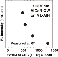
Fig. 2. PL intensity of AlGaN-QWs fabricated on ML-AlN buffer layer on sapphire as a function of XRC  FWHM.
FWHM.
Download figure:
Standard image High-resolution imageThe quaternary alloy InAlGaN is attracting considerable attention as a candidate material for realizing UV-LEDs, since efficient UV emission as well as higher hole concentrations can be realized due to In incorporation effects.2,11–14) Electron–hole pairs localized in the low-potential valley emit before they are trapped in nonradiative centers induced by dislocations. Therefore, the advantage of In incorporation is that the emission efficiency is less sensitive to TDD. We have described the advantages of the use of the quaternary InAlGaN alloy in Refs. 2, 11, 12, and 17.
Figure 3 summarizes the wavelength dependence of the ratio of the integrated PL intensity [PL measured at RT against PL measured at low temperature (usually below 20 K)] investigated in 2008,17) which is related to IQE. IQE of 340 nm InAlGaN QW was estimated to be 30–50%, even when we use a high-TDD template (TDD ∼ 2 × 1010 cm−2). However, IQE was reduced to below 2% for short-wavelength (280 nm) QWs. On the other hand, we achieved high IQE by introducing low-TDD ML-AlN templates. The ratios of the integrated PL intensity obtained for 280 nm QWs were approximately 30 and 86% for an AlGaN QW and an InAlGaN QW, respectively, when we use low-TDD ML-AlN templates (TDD ∼ 7 × 108 cm−2). The IQE at RT can also be estimated from the PL intensity observed at RT. We observed higher IQE values (50–60%) for AlGaN QWs by realizing a reduction of the TDD and by optimizing the AlGaN growth conditions.

Fig. 3. Wavelength dependence of the ratio of the integrated PL intensity (PL measured at RT against PL measured at low temperature) for AlGaN and quaternary InAlGaN QWs fabricated on conventional high-TDD AlN and on low-TDD ML-AlN templates on sapphire substrates.
Download figure:
Standard image High-resolution imageAlGaN and quaternary InAlGaN DUV LEDs were fabricated on low-TDD ML-AlN templates.16–22) Figure 4 shows a schematic of the structure and cross-sectional TEM images of an AlGaN-based DUV LED fabricated on a sapphire substrate. High-Al-composition AlGaN layers were used to obtain short-wavelength DUV emissions. A typical LED structure consisted of an approximately 4-µm-thick undoped ML-AlN buffer layer grown on sapphire, a 2-µm-thick Si-doped AlGaN bufferlayer, followed by a 3-layer undoped MQW region consisting of approximately 1.5-nm-thick AlGaN wells and 7-nm-thick AlGaN barriers, an approximately 20-nm-thick undoped AlGaN barrier, 6 pairs of Mg-doped AlGaN/AlGaN MQB EBLs, a 10-nm-thick Mg-doped AlGaN p-layer, and a Mg-doped GaN contact layer. The quantum well thickness was varied within the range between 1.3 and 2 nm. Thin quantum wells are preferable for AlGaN QWs to suppress the effects of large piezoelectric fields in the well. Ni/Au electrodes were used for both n-type and p-type electrodes. The typical size of the p-type electrode was 300 × 300 µm2. The output power that radiated into the back of the LED was measured using a Si photodetector located behind the LED sample, which was calibrated to measure the luminous flux so that the output power of a fabricated flip-chip LED device gives an accurate value. The output power of the flip-chip LED was measured precisely using an integratedsphere system.23) The LEDs were measured under "bare wafer" or "flip-chip" conditions. The forward voltages (Vf) of the bare wafer and the flip-chip samples with an injection current of 20 mA were approximately 15 and 8.3 V, respectively.

Fig. 4. Schematic structure and cross-sectional TEM image of a typical AlGaN-QW DUV LED fabricated on a sapphire substrate.
Download figure:
Standard image High-resolution imageFigure 5 shows the electroluminescence (EL) spectra of the fabricated AlGaN and InAlGaN MQW LEDs with emission wavelengths between 222 and 351 nm, all measured at RT with an injection current of approximately 50 mA. As can be seen in Fig. 5, single-peak operation was obtained for every sample. We obtained single-peak EL spectra, even for sub-230-nm-wavelength LEDs. The deep-level emissions were two orders of magnitude smaller than that of the main peak.
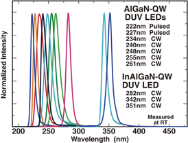
Fig. 5. (Color) EL spectra of fabricated AlGaN and quaternary InAlGaN-QW LEDs with emission wavelengths between 222 and 351 nm, all measured at RT with an injection current of approximately 50 mA.
Download figure:
Standard image High-resolution imageThe output power of the 227 nm LED was 0.15 mW at an injection current of 30 mA, and the maximum EQE was 0.2% under RT pulsed operation.19) The pulse width and the repetition frequency were 3 µs and 10 KHz, respectively. We also obtained single-peak operation of a 222 nm DUV LED, which is the shortest reported wavelength for an AlGaN LED. The output power of the 222 nm LED was 0.14 µW at an injection current of 80 mA, and the maximum EQE was 0.003% under RT pulse operation.20)
It has been reported that "normal" c-axis direction emission (vertical emission) is difficult to obtain from an AlN(0001) or a high-Al-content AlGaN surface, because the optical transition between the conduction band and the top of the valence band is mainly only allowed for light that has its electric field parallel to the c-axis direction of AlN (E ∥ c).9) The suppression of the vertical emission is a significant problem for AlGaN-based DUV LEDs, because it results in a reduction in the light extraction efficiency. Several groups have reported that vertical c-axis emission is suppressed for high-Al-content AlGaN QWs.40,41) We demonstrated that "normal" c-axis-direction emission (vertical emission) can be obtained, even for short-wavelength (222 nm) LEDs with a high-Al-content AlGaN QW.20) It was found that vertical c-axis emission can be obtained for an AlGaN-QW LED on AlN/sapphire, even when the Al content of the AlGaN QW is as high as 83%.
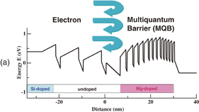
Despite achieving high IQE in DUV as mentioned above, EQE of the LED was still as low as 1–2%.17) The low EQE figures for AlGaN DUV LEDs compared with those for InGaN blue LEDs are a result of the low EIE due to electron leakage caused by low hole concentrations in the p-type AlGaN layers, as well as inferior LEE. We have introduced a MQB as an EBL in an AlGaN-QW LED, and have consequently achieved a marked increase in EIE.18) Figure 6 shows a schematic image of the enhancement of EIE caused by using an MQB. A large barrier height is required for the EBL to obtain a sufficiently high EIE. We have tried using high-Al-content (Al > 0.95) AlGaN layers for the EBL,18–20) but the barrier height of these EBLs is still insufficient to obtain the desired high EIE values. Indeed, EIE is estimated to be particularly low (<20%) for short-wavelength AlGaN LEDs (<250 nm). Such a material limitation can be overcome by enhancing the "effective" barrier height through the introduction of an MQB, which causes multireflection effects in the wavefunctions. The MQB was predicted theoretically by Iga et al. in 1986,42) and the effects were demonstrated experimentally in GaInP/AlInP red laser diodes (LDs).43) It was shown by calculation that the "effective" electron barrier height of an MQB in comparison with a conventional single-barrier EBL is increased by 2 times maximally for an AlGaN/AlGaN MQB with a thickness modulation design. We investigated experimentally an appropriate MQB structure for use with 250-nm-band DUV LEDs (as shown in the cross-sectional TEM image in Fig. 4).
Download figure:
Standard image High-resolution image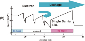
Fig. 6. (Color) Schematic image of electron injection into QWs in AlGaN-based DUV LEDs using (a) a conventional single barrier EBL and (b) an MQB.
Download figure:
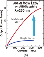
Standard image High-resolution imageFigure 7 shows the current vs output power (I–L) and current vs EQE (ηext) characteristics of a 250 nm AlGaN-MQW LED with either an MQB or a single-barrier EBL, both measured under RT cw operation. Significant increases in output power and EQE were observed when the single-barrier EBL was replaced by the MQB. The maximum output powers of 250 nm LEDs with the MQB and with the single-barrier EBL were 15 and 2.2 mW, respectively. EQE of a 250 nm LED was increased by approximately 4 times by the introduction of the MQB. From Fig. 7, we have estimated that the EIE of the 250 nm LED was improved from approximately 25% to more than 80% by using the MQB. The enhancement of EIE when an MQB was incorporated was especially high for short-wavelength DUV LEDs. Figure 8 summarizes the wavelength dependence of EQE for AlGaN DUV LEDs with MQBs and single-barrier EBLs. The enhancement factors of the EQEs when an MQB was introduced are approximately 10, 4, and 3 times for 235, 250, and 270 nm AlGaN LEDs, respectively.
Download figure:
Standard image High-resolution image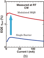
Fig. 7. (Color) (a) Current vs output power (I–L) and (b) current vs EQE (ηext) characteristics of 250 nm AlGaN-QW DUV LEDs with an MQB and a single-barrier EBL.
Download figure:
Standard image High-resolution image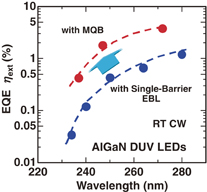
Fig. 8. (Color) Wavelength dependence of EQE of an AlGaN-QW DUV LED with an MQB and a single-barrier EBL.
Download figure:
Standard image High-resolution imageFigure 9 summarizes the maximum output powers of AlGaN and InAlGaN-based DUV LEDs fabricated on low-TDD ML-AlN templates that were achieved by the RIKEN group between 2007 and 2012.16–22) We have achieved significant increases in the EQE and output powers of AlGaN-based DUV LEDs by introducing low-TDD AlN templates and MQB electron-blocking layers. The maximum output powers obtained were 15–33 mW for 245–270 nm single-chip LEDs. These achievements will contribute to accelerating the practical application of DUV LED, and to expanding them to a wide range of applications.
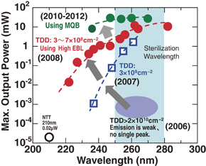
Fig. 9. (Color) Maximum output power of AlGaN and InAlGaN-based DUV LEDs fabricated on low-TDD ML-AlN templates achieved by the RIKEN group between 2007 and 2012.16–22)
Download figure:
Standard image High-resolution image4. Design of future DUV LEDs with high LEE
The improvement in LEE of a DUV LED is a particularly important subject for future research, however, it is not so easy because of the lack of suitable transparent contact layers, transparent p-type electrodes, or highly reflective p-type electrodes.
Figure 10 shows schematic images of the improvement in LEE of an AlGaN DUV LED that can be achieved by replacing the conventional structure by the novel LED structure proposed in this work. In a conventional DUV LED, the QW emission in the upward direction is completely absorbed by the p-GaN contact layer. The DUV emission in the downward direction is reflected by the sapphire/air interface (16% of the downward light is extracted and 84% of the downward light is reflected mainly by a total reflection). As a result, LEE of a conventional DUV LED is reduced to around 8%.
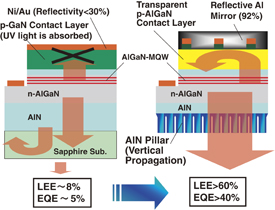
Fig. 10. (Color) Schematic images of the improvement in LEE of an AlGaN DUV LED by introducing a transparent p-AlGaN contact layer, a highly reflective p-type electrode, and a vertical-light-propagation AlN pillar array.
Download figure:
Standard image High-resolution imageTo realize high LEE, the combination of a transparent contact layer, a highly reflective p-type electrode, and a vertical light-propagation photonic structure is desirable. Recently, we have succeeded in fabricating a DUV LED with a high-Al-content p-AlGaN contact layer. We found that the p-AlGaN can act as a highly transparent p-type contact layer. The reflectance of a conventional Ni/Au p-electrode is low (<30%) and is not useful as a highly reflective mirror. The reflectance of Al in DUV is 92%, but Ohmic contacts are difficult to obtain. The introduction of a mesh-type electrode with Al mirror windows is one of the solutions for a highly reflective p-type electrode, as shown on the right of Fig. 10.
If the reflectivity of the p-type electrode is not sufficiently high (∼80%), a photonic structure with a vertical light-propagation property is required to extract the light with the minimum number of reflections. In other words, efficient light coupling into a photonic structure such as a pillar array is important for obtaining efficient light extraction.
LEE of a AlGaN DUV LED similar to we proposed was investigated by Ryu et al.44) based on the basis of finite-difference time-domain (FDTD) simulations. They also concluded from the calculation that the combination of a vertical LED geometry with a photonic nanostructure and a transparent p-AlGaN contact layer is important for obtaining high LEE in AlGaN DUV LEDs. They demonstrated that LEE of the vertical AlGaN DUV LED is improved by about ten times, when the thickness of the p-GaN contact layer is reduced from 25 nm to zero. They also demonstrated from the simulation that a maximum LEE as high as 72% can be obtained for the transverse-electric (TE) mode, if a transparent p-AlGaN contact layer is introduced in the vertical LEDs. Such results match well with our proposal.
We will demonstrate a very simple estimation of LEE for a proposed DUV LED. We assume that the equivalent reflectance for the upward-direction light is 80%, which is determined by the reflectivity of a p-electrode and the absorption through a p-AlGaN contact layer. We also assume that the equivalent coupling coefficient of the downward light into a pillar array is 40%. In other words, 40% of the downward light can be effectively extracted through the pillar array. Of course, they are average values taking into account all propagating light to every direction. At first, 50% light is emitted from the QW toward the downward direction and 40% light is reflected and returned by the p-electrode, then 90% light reaches in front of a pillar array. The amount of the first-time extraction light through the pillar array is calculated to be 90% × 0.4 = 36%. Then, 54% light is reflected by the pillar array. The amount of the second-time extraction light through the pillar array is obtained as 54% × 0.8 × 0.4 = 17.3%. By the same manner, the amounts of the third- and fourth-time extraction light are calculated as 8.3 and 4%, respectively. By integrating the amounts of the first- to the third-time extraction light, we can obtain high LEE of more than 61.6%. The equivalent coupling coefficient of 40% is considered to be reasonable by comparing with FDTD results. Through the above estimations, we can obtain high LEE with the minimum number of reflections by using the structure shown on the right of Fig. 10.
We demonstrated a DUV LED with a highly transparent p-AlGaN contact layer. The LED structure used for the experiment is shown in Fig. 11. The emission wavelength of the QW was 277 nm, and the Al composition of the p-AlGaN contact layer was varied between 60 and 63% (corresponding compositional wavelengths were 270–265 nm). We confirmed that the transparency of a 100-nm-thick p-AlGaN layer with an Al composition of 60% is higher than 94% for 279 nm DUV light, as measured using a spectrophotometer. As a p-type electrode, we replaced the conventional Ni (25 nm)/Au (150 nm) structure with a highly reflective Ni (1 nm)/Al (150 nm). Current injection was made possible by inserting a very thin Ni layer (<1 nm) between the Al layer and the p-AlGaN layer. In the actual experiment, the reflectivity of the p-type electrode was increased from 30 to 64% by replacing the conventional Ni (25 nm)/Au (150 nm) electrode with a Ni (1 nm)/Al (150 nm) electrode.

Fig. 11. Schematic structure of an AlGaN-QW DUV LED with a transparent p-AlGaN contact layer and a highly reflective Ni/Al p-electrode.
Download figure:
Standard image High-resolution imageFigure 12 shows the current vs EQE (ηext) characteristics of 277 nm AlGaN-MQW DUV LEDs with transparent p-AlGaN contact layers and a conventional Ni/Au p-electrode, measured under RT cw operation. We achieved the operation of DUV LEDs with high-Al-composition (60–63%) p-AlGaN contact layers. The maximum EQEs that we obtained were 3.1 and 2.8% for Al compositions of 60 and 63%, respectively, of the p-AlGaN contact layer. We found that direct contact between high-Al-content p-AlGaN and a Ni/Au or a Ni/Al electrode is useful for DUV LEDs, despite the quite low hole concentration of p-AlGaN.
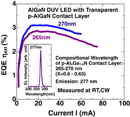
Fig. 12. Current vs EQE (ηext) characteristics of 277 nm AlGaN-MQW DUV LEDs with transparent p-AlGaN contact layers and a conventional Ni/Au p-electrode, measured under RT cw operation.
Download figure:
Standard image High-resolution imageFigure 13 shows the current vs EQE (ηext) characteristics of 279 nm AlGaN-MQW DUV LEDs with transparent p-AlGaN contact layers, comparing them with conventional Ni/Au and highly reflective Ni/Al p-electrodes measured under RT cw operation. EQE was significantly increased from 4 to 7% (by 1.7 times) owing to the increase in LEE induced by replacing the conventional Ni/Au p-electrode with a highly reflective Ni/Al electrode. We can estimate that the transparency of the p-AlGaN contact layer is higher than 95% from the enhancement factor of LEE. The LEE enhancement factors that were achieved in 265–279 nm DUV LEDs by replacing the Ni/Au p-electrode with the highly reflective Ni/Al electrode were approximately 1.3–1.7.
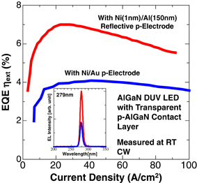
Fig. 13. Current vs EQE (ηext) characteristics of 279 nm AlGaN-MQW DUV LEDs with transparent p-AlGaN contact layers in comparison with conventional Ni/Au and highly reflective Ni/Al p-electrodes, measured under RT cw operation.
Download figure:
Standard image High-resolution imageWe observed an increase in the forward voltage (Vf) when p-GaN was replaced with a transparent p-AlGaN contact layer. Vf at an injection current of 5 mA increased from 11 to 17 V for a bare wafer DUV LED when the contact layer was changed from p-GaN to p-AlGaN. Therefore, the high resistivity of p-contacts caused by the low hole concentration is still a problem for the use of p-AlGaN contact layers. The increase in Vf causes a reduction in the wall-plug efficiency (WPE) of the device. We aim to improve Vf by using mesh-type p-electrodes, as we proposed in Fig. 10.
To achieve high LEE, we are developing a connected pillar AlN buffer on a patterned sapphire substrate (PSS). Figure 14 shows (a) a scanning electron microscopy (SEM) image of the surface of the PSS, (b) an optical microscopy surface image and (c) an SEM bird's-eye view of an AlN pillar array, and (d) an SEM bird's-eye view of a connected pillar AlN buffer layer. The period of the triangular lattice of the PSS used in this experiment was around 3 µm. The PSS was fabricated by nanoimprinting and an inductively coupled plasma (ICP) dry-etching technique. We have succeeded in growing high-aspect-ratio hexagonal AlN pillar arrays on PSS under high-temperature and low-V/III-ratio growth conditions. The use of such a pillar array structure would be quite effective for obtaining high LEE in DUV LEDs. The AlN pillar array was embedded in a flat surface by an overgrowth process under low-V/III-ratio growth conditions, as shown in Fig. 14(d). We have fabricated a 270 nm DUV LED on a connected pillar AlN buffer, and obtained a maximum EQE of 0.4% and a cw output power of 5 mW. We are trying to improve the efficiency of the LEDs by improving the surface roughness of the pillar buffer.
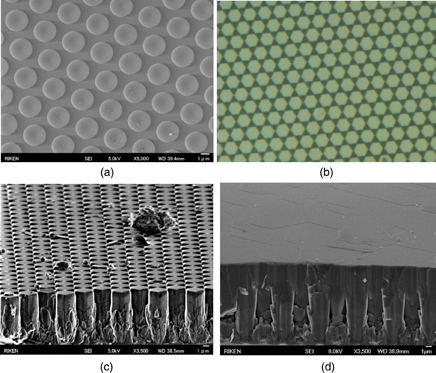
Fig. 14. (a) SEM image of the surface of a PSS, (b) optical microscopy surface image and (c) SEM bird's-eye view of an AlN pillar array grown on the PSS, and (d) SEM bird's-eye view of a pillar AlN buffer layer fabricated by lateral overgrowth.
Download figure:
Standard image High-resolution imageWe need the remove the sapphire wafer to fabricate the high-LEE LED structure shown in Fig. 10. The process of removing the sapphire from the AlN layer by a laser lift-off (LLO) method is not very suitable for high-efficiency devices because of the damage it induces in the epitaxial layers. Si substrates can be easily removed from nitride epilayers by wet-chemical etching. The use of a Si substrate is one of the solutions for the damage-free removal of the substrate. The fabrication of a DUV LED on a Si wafer has also other advantages, i.e., large-area and low-cost devices are possible, and a vertical LED structure is easily fabricated by removing the Si substrate. However, the crystal growth of AlN buffer layers on Si substrates is relatively difficult owing to the generation of surface cracks caused by the fact that the thermal expansion coefficient of Si is much smaller than that of AlN.
We have developed AlGaN and quaternary InAlGaN DUV LEDs on Si substrates.45,46) To obtain a crack-free AlN buffer layer on a Si substrate, we fabricated AlN layers by the ELO method.46) Figure 15 shows (a) a cross-sectional SEM image of an ELO AlN buffer layer on Si and (b) the structure and spectrum of a DUV LED fabricated on an ELO AlN-on-Si substrate. We have succeeded in the first demonstration of a DUV LED fabricated on a Si substrate. The emission wavelength of the LED was 256 nm under RT cw operation.46) We are planning to realize the proposed structure as shown in Fig. 10 by introducing these techniques, with the aim of achieving a marked improvement in LEE for DUV LEDs. We hope that the application of such devices to fields involving sterilization will be widely expanded through the achievement of high-efficiency DUV LEDs in the near future.

Download figure:
Standard image High-resolution image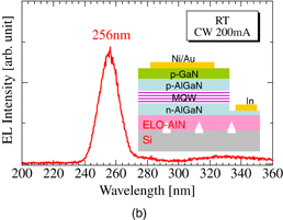
Fig. 15. (a) Cross-sectional SEM image of an ELO AlN buffer layer on Si and (b) structure and spectrum of a DUV LED fabricated on ELO AlN on a Si substrate.46)
Download figure:
Standard image High-resolution image
5. Conclusions
We demonstrated the recent progress in AlGaN-based DUV LEDs, which has been achieved by the development of crystal growth techniques for wide-bandgap AlN and AlGaN. Significant increases in IQE have been achieved for AlGaN-QW DUV emissions by using low-TDD AlN on sapphire grown by an NH3 pulsed-flow multilayer growth method. 222–351 nm DUV LEDs have been achieved using the high-IQE emission layers. EIE of the DUV LED was significantly increased by controlling the electron flow using an MQB. We also demonstrated the improvement of LEE by using a transparent p-AlGaN contact layer and a highly reflective p-electrode. The maximum EQE obtained was 7% for a 279 nm DUV LED. EQE could be increased up to several tens of percent in the near future by improving LEE by utilizing transparent contact layers and pillar array buffer layers.
Acknowledgments
We would like to express our sincere thanks to Dr. K. Tsubaki, Dr. J. Sakai, Dr. T. Takano, Dr. T. Mino, and Mr. N. Noguchi of Panasonic Corporation, for fruitful discussions and cooperation with the experiments.