Abstract
This paper reviews the various types of structural defects observed by transmission electron microscopy in GaN heteroepitaxial layers grown on foreign substrates and homoepitaxial layers grown on bulk GaN substrates. The structural perfection of these layers is compared to the platelet self-standing crystals grown by high nitrogen pressure solution. Defects in undoped and Mg doped GaN are discussed. Some models explaining the formation of inversion domains in heavily Mg doped layers that are possible defects responsible for the difficulties of p-doping in GaN are also reviewed.
Export citation and abstract BibTeX RIS
1. Introduction
In recent years GaN and related III–nitride alloys have demonstrated unique properties that are required for the design and production of light limiting diodes and lasers operating in the UV to visible spectral range.1–3) Such devices with similar performance are not achievable by other materials. Applications of III–nitrides to devices such as continuous wave (CW) lasers require materials with low defect density. However, when research on III–nitrides started at the end 1990s large-size bulk GaN substrates was not available. Most commonly used substrates for thin film growth were sapphire and 6H SiC. Molecular beam epitaxy (MBE),4,5) metal–organic chemical vapor deposition (MOCVD),6,7) or hydride vapor phase epitaxy (HVPE)8–10) methods were used for the hetroepitaxial growth of group III–nitrides thin films. Because of the much higher cost of SiC, sapphire (Al2O3) became the most widely used substrate. Due to the large lattice mismatch between the substrate and GaN (∼14%) or SiC (∼3.6%) high defect density appeared in these layers.
Parallel with the advance in MBE, MOCVD, and HVPE growth a lot of efforts was devoted to develop bulk GaN crystals in order to eliminate misfit defects due to hetero-epitaxy on foreign substrates. There are several challenges to grow bulk crystals that include: high melting temperature of most nitrides, low sublimation/decomposition temperature relative to the melting temperatures, very high equilibrium vapor pressure at moderate temperatures and also low solubility in acids, bases and the majority of inorganic elements and compounds. Crystallization from solution (either sodium flax method or in supercritical ammonia called ammonothermal method),11–13) high nitrogen pressure solution (HNPS)14,15) or combination of HNPS and HVPE methods by using the multi-feed-seed (MFS) configuration16,17) allowed large size free standing GaN with much higher quality. Some defects might be still present in these bulk crystals, but their nature is different and their density is negligible in comparison with the MOVPE or HVPE grown layers on foreign substrates. In order to decrease the density of these defects or completely eliminate them, the nature of these defects needs to be understood. Specific methods might be applied to decrease the density of these defects to the level that the newly grown material can be used for light emitting diodes (LEDs) or laser diodes (LDs) and detailed review of these methods can be found in references.18,19) In the present review paper structural defects in GaN will be reviewed.
2. Heteroepitaxial growth
2.1. Dislocations in GaN grown on sapphire
The growth of a heteroepitaxial layer on any substrate will depend strongly on three parameters: lattice mismatch, layer thickness and thermal expansion parameter between the substrate and the layer. When the lattice misfit is small, stress in the layer can be relieved through surface undulation with the increase of the layer thickness. With an increase of lattice mismatch a layer under compressive (or tensile) strain will be formed and the in-plane unit cells will match the substrate and the unit cells along the growth direction will expand (or contract). With further increase of the layer thickness, the strain needs to be released and a misfit dislocation in the plane of the interface will be introduced. There are several mechanisms leading to the formation of a dislocation in the layer. The most common one being the propagation of a dislocation running from the substrate to the layer. A dislocation that was originally present in the substrate will bend at the interface forming a misfit dislocation segment and then propagate to the layer surfaces as a threading dislocation. If there are no pre-existing dislocations in the substrate, then a half loop will be introduced at the layer surface that will propagate to the interface plane forming a misfit dislocation. The arms of this loop will form threading dislocations.20) Such defects are called line defects. One can distinguish perfect and partial dislocations. The latter one is associated with a planar defect called stacking fault. There are three different types of perfect dislocations that are characterized by line direction and a Burgers vector.
For GaN grown on sapphire where the lattice mismatch can be as large as 14% three different Burgers vectors were revealed by transmission electron microscopy (TEM): 1/3〈1120〉 for an edge dislocation, 〈0001〉 for screw dislocation and 1/3〈1123〉 for mixed dislocations, assuming that the dislocation line is parallel to the c-axis. Jasinski and Liliental-Weber21) showed that for thin samples (up to 2.5 µm thick) all three types of dislocations (edge, screw and mixed) were present with comparable numbers. However, for the sample with larger thickness (5.5 µm and larger) the number of edge and screw dislocations was comparable, but the number of mixed dislocations was twice higher. Similar results, showing dominating number of mixed dislocations close to the sample surface, were also found in thick free-standing samples. For these samples the sapphire substrate was removed at the early stage of growth.
It was shown by Ponce et al.22) that at the start of the growth of GaN on sapphire, three-dimensional growth took place with many separate nucleation sites. Tilted or twisted grains were formed with grain boundary dislocations to accommodate tilt/twist between the grains. As a result of dislocation reactions some threading dislocations are formed and they propagate to the sample surface during the growth with dislocation line directions parallel to the c-axis. Close to the GaN/sapphire interface, there are many inclined dislocations (due to the island growth mode) that have higher probability to interact with each other. As the distance from the substrate increases, the number of inclined dislocations decreases compared to the number of dislocations parallel to the c-axis because the roughness of the growth surface decreases. As a result, the probability of dislocation interactions decreases and the process of dislocation density reduction slows down.
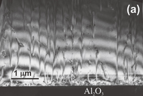
Jasinski and Liliental-Weber21) showed, using TEM, that in GaN samples grown by MOCVD on sapphire estimated density of dislocations was in the range 1010 to 106 cm−2 depending on the layer thickness. Further decrease of dislocation density for thicker layers becomes increasingly difficult, since their line directions are primarily parallel to the c-axis, as shown in Fig. 1(a), and the average separation between them is greater. This reduces significantly the probability of interactions between dislocations. Taking this into account the growth of thicker and thicker layers not always leads to the reduction in dislocation density. If strain remains in the layer, then cracking will take place as shown in Fig. 2.20) However, Tachikawa and Yamaguchi23) and later Speck et al.24) proposed a model adapted from Sheldon et al.25) used for cubic materials and showed that density of threading dislocations in relatively thick layers is inversely proportional to the film thickness. This model was also applied by Jasinski et al.21) to analyze cross-sectional TEM results on HVPE GaN layers and found that the density of dislocations decreases from 9 × 109 cm−2 for the sample thickness of 1.5 µm, shown in Fig. 1(b), to (2–8) × 106 cm−2 for the sample thickness of 300–750 µm. Reasonable agreement was obtained with earlier work of Mathis et al.26) who analyzed experimental data on HVPE GaN reported by Golan et al.27) obtained on HVPE GaN using plan-view TEM and X-ray diffraction measurements. Mathis et al.26) emphasized that efficiency of dislocation reduction strongly depends on the initial dislocation distribution and their Burgers vector.
Download figure:
Standard image High-resolution image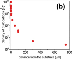
Fig. 1. (a) TEM micrograph from the GaN cross-section sample grown by HVPE on c-plane sapphire. Note some decrease of dislocation density with the sample thickness and also that majority of dislocations in the upper part of the sample have line direction parallel to the c-axis. (b) Density of dislocations (linear scale) for different sample thickness.
Download figure:
Standard image High-resolution image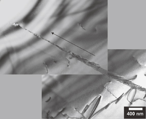
Fig. 2. A crack formed in the homoepitaxial GaN sample grown by HVPE. The arrow indicates the c-direction. Note some dislocations formed in the vicinity of the crack.
Download figure:
Standard image High-resolution image2.2. Pinholes and nanotubes
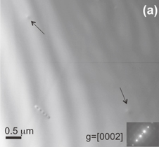
It is well known that deleterious defects in SiC are microtubes that are hollow tubes extending along the growth direction. They have rather a large size extending from a micrometer to several micrometers and their density is in the range of 100 to 1000 cm−2.28,29) In GaN grown on sapphire similar features, but with much smaller diameter (3–1500 nm), are also observed. On TEM micrographs in plan-view configurations they appear as slightly elongated hexagons (Fig. 3), but their density in some materials might reach as high as 107 cm−2. However, when observed in cross-section one can distinguish two different types of these defects. Some of them are elongated along c-axis, have a constant diameter, are empty inside, and completely embedded in the layer, as shown in Fig. 4(a). Such defects are called nanotubes. Their diameter can be in the range of 2–40 nm. Other defects, shown in Fig. 4(b), called pinholes, have a triangular cross-section and extend to the sample surface forming some indentation.30) Their diameter at the surface is ranging from 300–800 nm. Northrup et al.31) suggested that these defects might be associated with dislocations, mainly screw dislocations, but in many cases these defects can be found also in dislocation free areas.30,32,33) Therefore, it is not clear if dislocations that are seen attached to these defects are responsible for their nucleation or they are attracted to these empty holes to decrease the total dislocation line energy.

Fig. 3. (a) Plan-view micrograph (in [0001] projection) showing a pinhole, formed in the subsurface area of the GaN sample grown by MOCVD, overlapped with the open core screw dislocation (marked by the arrow in the center of the pinhole). Note much larger diameter of the pinhole in comparison with the diameter of the core-less dislocation. (b) A pinhole formed in the subsurface area of the GaN probably not attached to any dislocation. (c) A full core screw dislocation observed edge-on in [0001] projection. Burgers contours are outlined in (b) and (c) showing no displacement vector.
Download figure:
Standard image High-resolution image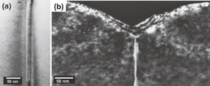
Fig. 4. (a) Cross-section micrograph showing a nanotube along the growth direction aligned with a screw dislocation present in the GaN sample grown by MOCVD. Note that this nanotube starts from the triangular (V-shape) pinhole, and then changes to the tubular shape. The small arrow indicates the area where this nanotube terminates within the layer despite that the dislocation still propagates to the upper part of the sample. (b) V-shape pinhole formed in the subsurface of the layer propagating to the sample surface. This pinhole is attached to a screw dislocation.
Download figure:
Standard image High-resolution imageFrank34) suggested that a dislocation with a large Burgers vector could lower total line energy if its core is empty. The studies by Liliental-Weber et al. showed30,35) that empty core of a screw dislocation is not larger than 0.8 nm, as can be seen in Fig. 3, but a diameter of a nanotube attached to the dislocation is about 10–15 times larger. Therefore, a different mechanism must lead to the formation of a nanotube. These researchers30,35) showed that more pinholes are observed in MOCVD grown layers than in MBE layers. This would suggest that the formation of nanotube defects might be related to some impurities (or dopants), since no correlation between the density of dislocation and nanotubes have been found. Liliental-Weber et al.36) showed that in GaN an increase of Si doping from 9 × 10¹⁶ to 1 × 1019 cm−3 leads to a decrease of dislocation density from 1 × 10¹⁰ to 3 × 109 cm−2. However, the density of nanotubes increased from 1 × 10⁶ to (6–8) × 107 cm−2.30,32,35,36) Also, in the layers where the oxygen content increased from 5 × 10¹⁷ to 4 × 1018 cm−3 the density of pinholes increased from 1 × 10⁷ to 3 × 107 cm−2 with no change in dislocation density.32) Similar increase of nanotube and pinhole density was observed when other dopants were used (like Mg) or when diluted ternaries (AlGaN, InGaN) were grown. This was confirmed by Herera et al.33) who suggested that pinhole formation should be related to the residual stress in the films induced by doping. Both these defects: pinholes and nanotubes originate from the V shape features (Fig. 4) with arms formed on {1011} planes with about 56° between them. These are the slowest growth planes and can be easily poisoned by impurities. Therefore, pinholes are grown on these planes. However, the nanotubes also originate from the small V shape features but later change to tubular growth along c-axis, as can be seen in Fig. 4(a). It was suggested30) that the origin of nanotubes and pinholes may be related to growth kinetics on particular crystallographic planes and impurity poisoning of growth steps, especially on slow growth {1011} planes. Formation of these defects most probably can be eliminated, by reduction of impurity level and by choosing proper substrate orientation. However, it will be more difficult to eliminate them in ternary compounds.
3. Planar defects
GaN can be grown either in wurtzite or sphalerite polytype37) with the wurtzite structure being more common. In both sublattices (0002) planes are close packed with stacking planes  AaBbAaBb
 where capital letters correspond to Ga layers and small letters to N layers forming a stacking unit bilayers. In wurtzite structure these stacking are in two different positions shifted by 0.377c along [0001]. If small letters are omitted the hexagonal stacking can be described as
  ABABAB
 and capital letters represent Ga–N atomic bilayers. In the sphalerite structure these stacking are arranged in ABCABCABC sequence along the [111] direction. The wurtzite and sphalerite polytpes can be intermittent since small growth instability during the growth of the wurtzite polytype can shift the next growth stacking to C position forming locally sphalerite (zinc blende) structure. In the sphalerite polytype removal (or addition) of one stacking can lead locally to the formation of wurtzite polytype. Therefore, basal plane stacking fault (BSF) in the wurtzite structure is a local insertion of the ABC cubic structure within the usual
  ABABAB
 stacking sequence. An insertion of a zinc blende unit cell requires rotation of the bonds, e.g., the mirror symmetry for bond arrangement typical of the wurtzite structure is lost and it is locally converted to the zinc blende bond arrangement, where bonds are rotated 60° with respect to the nearest neighbor bonds.
There are three types of BSFs in a wurtzite structure shown in Fig. 5: two intrinsic: I1 and I2 and one extrinsic E.37,38) These faults differ by the number of inserted or removed basal planes and their formation energy is proportional to the number of inserted cubic layers. The I1 stacking fault can be described as  ABABABCBCBC
 with a single cubic stacking. Such a fault is bounded by a sessile Frank-Shockley dislocation with Burgers vector b = 1/6[2023]. The I1 fault is formed by the insertion or removal of c basal plane followed by 1/3[1100] or 1/3[1100] slip of the upper part of the GaN crystal with respect to the lower part. Examples of such type of the BSF were described earlier by Zakharov et al.38) for the growth of GaN on (1120)4H-SiC with AlN as a buffer layer. For this growth the orientation relationship between GaN/AlN/4H-SiC was described as (1120)GaN ∥ (1120)AlN ∥ (1120)4H-SiC. In this orientation GaN c-planes are arranged perpendicular to the sample surface, therefore it is easier to see these defects in plan-view configuration as thin lines when two-beam condition using g = [1100] was applied. These authors38) observed two different residual contrasts (dark and white) from partial dislocations delineating these planar defects, shown in Fig. 6, that suggested the formation of two different types of partial dislocations. Study of these partial dislocations gave the information concerning the type of stacking fault. These authors38) showed that dark contrast indicated the formation of the I1 fault and white of I2.

Fig. 5. Schematic drawing of the atomic arrangement in wurtzite GaN showing three different types of stacking fault. They are called I1, I2, and E, respectively, with one, two and three inserted sphalerite units within the wurtzite structure.
Download figure:
Standard image High-resolution image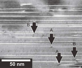
Fig. 6. Bright-field micrograph (g = 1100) of stacking faults (thin lines) formed on the basal plane of GaN. Note that partial dislocations terminating some of the SFs have different contrast: A-indicates black contrast (Frank partial dislocations characteristic of I1 SF) and B-with white contrast (Shockley partials characteristic of I2 SF).
Download figure:
Standard image High-resolution imageType I2 of BSFs should be delineated by Shockley partials with b = 1/3[1100] and can be described as ABABABCACA. They can be formed by 1/3(1100) shear of one part of a crystal with respect to the other or by dissociation of a perfect dislocation b = 1/3[1120] into two Shockley partials with b = 1/3[1100]. Zakharov et al.38) showed that despite the fact that the faults appeared as thin lines for imaging with g = [1100] they can be of different type, since partial dislocations delineating these faults have different contrast and are invisible for different diffraction vectors.
The insertion of an extra basal plane leads to the formation of E-type BSF that can be described as  ABABABCABABAB
 . This type of fault is bounded by Frank partials with b = 1/2[0001]. The formation energy γ of this fault is the largest and γE > γI2 > γI1.38) Despite that the formation energy of type I1 fault is the smallest among the three of them it requires the removal of a basal bilayer in addition to the basal shear of 1/3(1100). This fault can be formed during the growth process. On the other hand, I2 fault might be caused by some stress since it requires the movement of a glissile Shockley partial dislocation in the basal plane. The E fault might be formed by the precipitation of point defects on the basal plane and usually is surrounded by a dislocation loop. Stampfl and Van de Walle39) predicted the formation of an additional basal fault I3 with a sequence ABABCBABAB. This fault can be formed when either A or B bilayer occupies the "wrong" C position. According to their calculation the formation energy of this fault would be only slightly larger than I1 fault but smaller than I2.
It has been shown that BSFs might be terminated not only by partial dislocations, but can also be terminated by different planar defects formed on other planes. The most known defect is a prismatic stacking fault (PSF) described by Drum.40) Usually these defects are formed on {1210} planes with the displacement fault vector R = 1/2〈1011〉. These faults, shown in Fig. 7(a) terminate BSFs with stair-rod dislocations formed at the intersections of PSFs and BSFs. These faults were observed by Zakharov et al.38) in GaN grown on (1120) 4H-SiC. It was shown that in these samples the PSF faults, seen as thin lines, intersected the sample surface at 60° and were formed on (2110) and (1210) planes forming zig-zag structure. Alternating the defect plane might lead to a decrease of the total fault energy. Their density was estimated as 0.7 × 102 cm−1 and the size of the PSF seen in [0001] direction did not exceed 6–7 nm. Since the displacement vector of an I1 BSF and a PSF is different, the formation of a stair-rod dislocation is expected at the intersection of these two faults, schematically shown in Fig. 7(b).

Download figure:
Standard image High-resolution image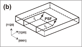
Fig. 7. (a) Cross-section micrograph of a PSF terminated by two I1 SFs. (b) Schematic drawing of a PSF with two I1 SFs. The arrow at the intersections of the PSF and I1 indicate stair-rod dislocations with the same value of the Burgers vector but with the opposite sign.
Download figure:
Standard image High-resolution image4. GaN growth polarity
GaN is a crystal without a center of symmetry, therefore a GaN layer grown on c-plane sapphire can have two different growth polarities, described as [0001] for Ga or [0001] for N. GaN layers grown along the 〈0001〉 direction have alternating layers of Ga and N that are connected with each other either by the three bonds between these atoms (inclined toward the growth direction) or by the single bond parallel to the growth direction. A single bond is always easier to break than the three bonds, therefore, the atom on the surface from which a single dangling bond points upward (along growth direction) determines the growth polarity. A layer has a Ga-growth polarity when the growth direction points from a Ga to a N atom and N-growth polarity when N to Ga bond points towards the growth direction, as shown in Fig. 8. However, the expression "surface termination" often used in the literature sometime can be rather ambiguous since depending on the growth condition (Ga- or N-rich) experimental results and theoretical predictions may show different surface reconstructions coming from the presence of Ga atoms forming an "adlayer" and this surface reconstruction will change depending on the growth condition (Ga- or N-rich) and will be not necessary representing the growth polarity.41–43)

Fig. 8. Schematic drawing of atomic positions in GaN along the c-axis: for N-growth polarity (left) and Ga-growth polarity (right). For simplicity only one inclined bond (instead of three) is shown.
Download figure:
Standard image High-resolution imageGrowth polarity strongly affects the surface structure and chemistry of group III–nitride and hence it is very important for the development of GaN devices. For example, strain and polar direction of GaN film determines the direction of the piezoelectric field44–46) that is crucial to the device performance. Designing of electronic devices such as thin film transistors and quantum wells47–50) with 〈0001〉 grown GaN thin films requires the consideration of the polar direction. Therefore, knowledge of the growth polarity and an understanding of the mechanism that determines the particular polar direction of group III–nitride and GaN in particular are of high importance.51–58)
There are several methods that can be used to determine the growth polarity. One of them is etching by using an aqueous solution of KOH at room temperature. This solution selectively attacks one polarity of GaN, whereas surface of the opposite polarity remains unaffected even when the sample is etched for 30 min. The sample surface that does not change during etching has Ga growth polarity.19,59,60) The successful use of KOH etching at room temperature for GaN polarity determination was also confirmed by Seelmann-Eggebert.61) However, this method cannot be applied to small areas, especially for the determination of small domains with the opposite growth polarity.
Another method for the determination of GaN growth polarity is coaxial impact collision ion scattering spectroscopy (CAICISS) analysis with the scattering angle 180°.62,63) CAICISS surface sensitivity is due to its broad shadow cone from its low (1–3 keV) ion energy and their analysis depth depends on the shape of the shadow cone determined by the H+ ion energy. Assignment of the growth polarity of GaN layers can be obtained by comparison of the experimental CAICISS signal intensities as a function of polar angle Q of incident He+ ions to the simulation based on tri-dimensional two-atom a triple-scattering model.64)
One of the best methods that can be used to determine the growth polarity is convergent beam electron diffraction (CBED).51–58) This method has also the unique advantage that it can be applied to very small volumes that cannot be studied by other methods. A dynamic approach with full CBED pattern of the [1100] pole is usually used, but a kinematic approach using a systematic (0002) row can be also applied. Since the GaN crystal is a non-centrosymmetric the intensity distribution within the (0002) and (0002) discs is different and this information can be used to determine the crystal polarity. As a reference, computer-simulated CBED patterns need to be calculated along the [1100] zone axis for a particular Ga–N bond arrangement and for different sample thicknesses for the acceleration voltage of the microscope used for the experiment (200 or 300 kV). The experimental and calculated patterns are then compared for the final determination of the growth polarity, as can be seen in Fig. 9. The central disc of such pattern carries the information about the sample thickness for a given accelerating voltage of the microscope. The intensity distribution within the (0002) and (0002) discs along the growth direction parallel to the c-axis gives the unique information about the growth polarity of a particular sample. To be sure that the growth polarity is assigned correctly CBED patterns should be taken in different defect free areas of the same sample that have a different thickness and results should be consistent. For the electron microscopes where the rotation angle between the diffraction pattern and the image of the crystal is changing, for different image magnifications, this rotation angle needs to be taken into account to have the correct arrangement of the (0002) and (0002) discs towards the diffraction planes. CBED patterns are very useful for the determination of the presence of small inversion domains, where other methods would be difficult to apply.57,65)
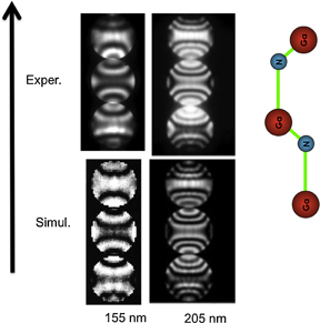
Fig. 9. Convergent beam electron diffraction for two different sample thickness (155 and 205 nm, respectively) of GaN grown with Ga polarity. Atomic arrangement along c-axis is presented.
Download figure:
Standard image High-resolution image5. Bulk "platelet" GaN crystals
As was shown earlier in Fig. 1(a) the growth of GaN on foreign substrates leads to high density of structural defects that are detrimental for devices. Especially application of GaN for devices such as CW lasers requires low defect density to ensure reliable operation at high current density. For this reason there is a large demand to develop bulk crystals in order to eliminate misfit defects formed in heteroepitaxy.
There are some promising methods for obtaining good quality GaN crystals: growth of thick layers from the vapor phase using HVPE8–10) or crystallization from solution (either the sodium flux method or in supercritical ammonia called the ammonothermal method).11–13) Parallel development of the HNPS growth achieved high quality platelet GaN crystals, but the size of these crystals was rather small.14,15)
These crystals have an elongated hexagon shape and crystallize with a wurtzite structure. Frequently the longest axis is along [1120] direction. In some cases, shown in Fig. 10(a), the samples are less elongated and the dimensions along [1120] and [1100] are similar and diameter of these crystals in most cases is about 1 cm but never larger than 3 cm. In all cases, the smallest dimension is in the c-axis direction. The ratio of plate width to thickness along the c-axis can reach as much as 100 times. This shows that growth along the c-axis is the slowest. Study of cross-section samples showed that one side of the plate is almost atomically flat while the opposite side is rough, as can seen on Fig. 10(b). These platelet crystals grow in Ga solution and need to be removed by etching. This would explain why one side of the crystal is more flat than the other since N flat side is more susceptible to etching. CBED study showed that the flat side of the crystal grew with N polarity and the rough side with Ga polarity.20,51–53)

Fig. 10. (a) Optical picture of the almost round GaN platelet sample placed on the millimeter paper with indicated [1120] direction. Most of these plates have a hexagonal shape with elongation along this direction. (b) A cross section micrograph from such a platelet showing different corrugation of both surfaces. The arrow indicates the direction of Ga-polarity. (c) Thin lines indicate the presence of stacking faults found close to the rough side of the sample. They are superimposed with dislocation loops (dark short segments). (d) Small Ga precipitates P with voids (lighter contrast) attached to the dislocation loops.
Download figure:
Standard image High-resolution imageTEM studies of the cross-section of the platelet crystals showed formation of planar defects in the subsurface of the rough side of the platelet. These planar defects did not extend more than 1/10 to 1/4 of the plate thickness. The opposite side of the plate did not show any extended defects. The planar defects appeared in the [1120] and [1100] directions as long straight lines that extended through the entire plate from edge to edge, shown in Fig. 10(c). Therefore, it was assumed that they were nucleated during the early stages of growth. The analysis of high resolution micrographs showed the presence of all three types of stacking faults with one, two or three zinc blende unit cells inserted. In the direct vicinity of these long stacking faults (at the next atomic basal plane layer) shown in Fig. 10(c), large interstitial-type dislocation loops with a diameter of 10–100 nm were found. Formation of a dislocation loop located on the atomic layer next to a high-energy stacking fault is energetically favorable, since an insertion of the additional layer converts locally the high-energy fault configuration into the low-energy type of fault. These dislocation loops are decorated by Ga precipitates about 5 nm in diameter, shown in Fig. 10(d) that are always associated with a small void. It is expected that formation of these loops result in a different strain within and outside the loop because of the surrounding dislocation line at the edges of these loops. Therefore, the dislocation core appears to act as the nucleation site for the excess of Ga leading to precipitation since all bulk crystals were grown under high N pressure in an atmosphere of excess Ga.
6. Homoepitaxial growth
6.1. MBE growth on "platelet" substrates
Liliental-Weber et al.52) showed TEM studies of homoepitaxial layers grown by MOCVD on the smooth (N-polarity) and rough (Ga-polarity) sides of the platelet bulk GaN substrates after earlier surface preparation for the growth. By using the CBED method they showed that homoepitaxial layers continue to grow with the same growth polarity as the substrate, but the layer quality and type of defects are different, depending on the substrate polarity. Layers grown on the smooth surface with N growth polarity show a dark contrast along the interface that most probably was related to some inhomogeneity and decomposition of the N-polar surface during the growth at 1050 °C growth since N polarity is more susceptible to decomposition.66) Z-contrast technique showed conglomeration of Ga atoms at this interface, which might be also related to Ga adatoms present there. Other defects, such as threading dislocations or inversion domains also originated at some corrugated islands identified at this interface as is shown in Figs. 11(a) and 11(b).
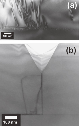
Fig. 11. TEM micrograph from the GaN sample grown by MOCD on the N-polarity platelet substrate. Note some irregularities present at this interface that gave the origin to the formation of dislocations in the layer, shown in (a) and vertical ID, shown in the center of (b). In the latter micrograph the pinhole is formed at the top of the inversion domain. Also in (b) dislocations that were formed far from the ID are attracted to the facet of the V-defect and during further growth interact with the ID.
Download figure:
Standard image High-resolution imageFor layers grown on the platelet substrates with N-growth polarity inversion domains (IDs), confirmed by CBED, were also found and shown in Fig. 11(b). Vertical domain boundaries were formed on {1100} planes and a shift of the (0001) lattice fringes, shown in Fig. 12, between the domain and the matrix was observed along the [0001] direction.52,56,67) This shift of lattice fringes is consistent with the work by Romano et al.56) who suggested the formation of an ID boundary with preserving Ga–N bonds at the interface. Such a bond arrangement would be energetically more favorable compared to the alternating Ga–Ga and N–N bond arrangement along a vertical domain boundary. Periodic four-atom and eight-atom rings would be expected at such boundary.
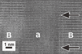
Fig. 12. High-resolution image of the vertical ID: a-represents the ID, B-the matrix. The arrows in the matrix on the right side indicate bending of the atomic planes at the matrix/ID interface.
Download figure:
Standard image High-resolution imageV-shape pinholes were formed on the top of such IDs.30,52) The sides of this V-shape pinhole are inclined 30° to the c-axis with an angle about 56° between the arms and are formed on {1011} planes. The latest work also provided information about an interaction between dislocations, inversion domains, and a pinhole and an example of such interaction can be seen in Fig. 11(b). It was shown that dislocations that were formed at the substrate/layer interface in the vicinity of the ID topped by a pinhole terminated on the facet of the pinhole. The pinhole facet can be treated as a free surface. When a dislocation appears in a close proximity of the V facet it bends toward the hole during further layer growth to shorten dislocation length and reduce total energy of the system. This is similar to the situation that a dislocation bends toward the sample surface, since a dislocation cannot end within the crystal (unless it is a dislocation loop or semi-loop).
Layers grown on the GaN substrate with Ga polarity did not show any threading defects. There was no dark contrast at the interface between the layer and the substrate and sometime it was difficult to determine the location of the interface. The authors reported52) that occasionally some interstitial type of dislocation loops could be found. However, a high density of pinholes (106–107 cm−2) was found in the layers grown on the platelet substrates for both polarities.
6.2. High pressure growth on HVPE substrate
GaN layers grown by HNPS with MFS configuration on HVPE substrates that were first grown on the sapphire substrate and then the sapphire was removed before the HNPS-MSF layers were grown.16,17) The main goal of this procedure is to obtain thick layers that can be later sliced for the application in devices. TEM studies by Liliental-Weber et al.68) of 90-µm-thick HNPS-MFS layers grown on 50-µm-thick HVPE substrate show that the majority of dislocations present in the substrate propagate to the HNPS-MFS grown layer. Some of them interact with each other; therefore, at the sample surface density of dislocations is much smaller. These dislocations in the layers, shown in Fig. 13, are decorated by the precipitates that were not observed in the HVPE substrate. These precipitates with voids [Figs. 14(a) and 14(b)] pointing toward the growth direction are amorphous and have tubular shape elongated along c-axis. The walls of these precipitates are formed on (1100) planes. By using electron energy loss spectroscopy (EELS) the authors showed that these precipitates are Ga precipitates, similarly as observed in the platelet crystals.20,51) They are not longer semi-spherical as in the platelet crystals and elongation of these precipitates along c-axis most probably is related to the directionality of the growth.
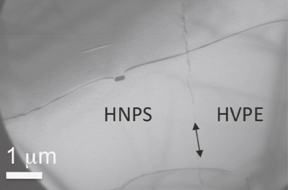
Fig. 13. TEM micrograph showing dislocations propagating from the HVPE substrate to the HNPS layer. Note a precipitate decorating a dislocation in the layer. The double arrow indicates the substrate/layer interface.
Download figure:
Standard image High-resolution image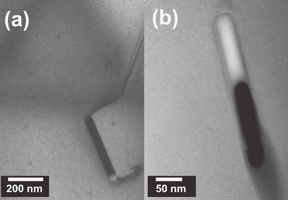
Fig. 14. Ga precipitates in the HNPS layer with attached voids pointing toward the growth direction. (a) Bright field image −a precipitate is shown with a dark contrast and a void with white contrast. (b) Z-contrast image, a precipitate is shown with white contrast and a void (empty space) with a dark contrast.
Download figure:
Standard image High-resolution imageBesides these dislocations decorated by Ga precipitates, much larger lens-shape features showing lighter contrast in bright field TEM images, shown in Fig. 15, were also observed in these HNPS-MFS layers. In the center of these lens features there is a void or other defect and are much thinner than the surrounding matrix. This suggests that either strain field or slightly different composition (possibly light elements) is responsible for this different thinning rate. Such features were never observed in the high-pressure platelet crystals or GaN layers grown by other methods.
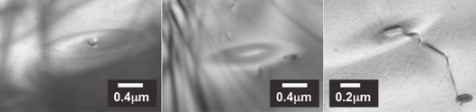
Fig. 15. Three micrographs showing lens shape defects present in the HNPS layers grown on HVPE substrates. These defects are formed around some voids or other defects.
Download figure:
Standard image High-resolution image6.3. HVPE growth on ammonothermal substrates
Liliental-Weber et al.68) investigated (960 µm) thick GaN layers grown by HVPE on 440-µm-thick ammonothermal substrates.12,69) In these samples it was very difficult to distinguish by TEM the layer/substrate interface, despite that the interface was visible under optical microscope. Only small difference in ion-mill thinning rate between the substrate and the layer could be observed, suggesting possible difference in impurity level in the substrate and the layer. Occasionally some cracks were formed at the interface during TEM sample preparation at almost the exact position where the interface was expected. This might suggest that the interfacial area is somehow weaker than the surrounding substrate or the homoepitaxial layer.
These authors68) using CBED studies showed that these HVPE layers have Ga growth polarity repeating the substrate polarity. Long dislocations observed in the HNPS-MFS layers grown on the HVPE substrates were not observed in the HVPE layers grown on the ammonothermal substrates. These layers can be considered as almost defect free. Small inclusions and some dislocations were occasionally observed with rather small density and examples are shown in Figs. 16(a) and 16(b), but their chemical composition was not identified. EELS studies showed only the presence of Ga and N but the concentration of other impurities was most probably below the detectability of the EELS method.
Download figure:
Standard image High-resolution image
Fig. 16. The cross-section micrograph showing the HVPE layer grown on the ammonothermal substrate. The layer has a very low defect density but occasionally small inclusions can be found [shown by arrows in (a) and (b)]. At the left lower corner in (a) a short dislocation is also visible. Diffraction vectors for these micrographs are indicated.
Download figure:
Standard image High-resolution image7. Mg doping
7.1. Defects in Mg doped high-pressure platelets and MOCVD grown GaN
Nominally undoped GaN layers are n-type70) while high quality p-GaN with high hole concentrationis is still difficult to achieve. Mg remains the most efficient p-dopant, but the free hole concentration is limited to 2 × 1018 cm−3 for Mg concentrations in the low 1019 cm−3. Further increase of Mg concentration, up to 1 × 1020 cm−3, leads to a decrease of the free hole concentration. This decrease is commonly interpreted as auto-compensation due to increased formation of N vacancies or vacancy complexes with Mg.71,72) The concentration of Mg at which hole concentration is saturated coincides with the threshold concentration for the formation of structural defects.58,73–79) These defects, in the form of pyramids or truncated pyramids, shown in Figs. 17(a) and 17(b), respectively, were first observed in bulk GaN crystals grown with Ga polarity under high nitrogen pressure.58,73,74) Shortly after this observation, similar defects were also observed in Mg doped MOCVD-grown thin films.75–79) Pyramids observed in the platelet crystals are almost one order of magnitude larger than those observed in MOCVD layers. Therefore, more accurate structural studies by TEM can be done on larger defects that do not overlap with the surrounding matrix in thin films transparent for electrons. Interpretation of high-resolution TEM micrographs of much smaller defects completely embedded in the matrix, present in the MOCVD layers, can be very difficult, especially for the determination of atomic positions.
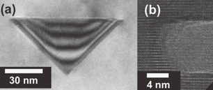
Fig. 17. (a) Pyramidal and (b) trapezoidal (truncated pyramids) inversion domains formed in the platelet GaN samples shown in cross-section in [1120] projection. Note much thinner areas inside the inversion domain suggesting different growth rate of the domain in comparison with the matrix (b).
Download figure:
Standard image High-resolution imageTEM studies showed that the type of defects in GaN platelet crystals grown under high N pressure and doped by Mg depends strongly on the growth polarity. In some crystals grown with [0001] N-polarity Mg-rich planar defects equally distributed at each 20th c-lattice plane (10.4 nm) were observed.58,73,74) Such defects, shown in Fig. 18 were never observed in these platelet crystals grown with Ga polarity. Selective area diffraction pattern (SAD) from these regularly spaced planar defects lead to additional diffraction spots dividing the (0001) lattice distance into 20 equal parts. Studies of these defects by Liliental-Weber et al. showed that these defects are flat inversion domains.58,73,74)
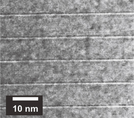
Fig. 18. Periodic arrangement of flat inversion domains found in GaN:Mg platelet sample grown with N-polarity.
Download figure:
Standard image High-resolution imageDifferent types of defects were observed for the growth with Ga polarity. In [1120] projection these defects are seen as triangles58,73,74,80,81) or trapezoids and are shown in Figs. 17(a) and 17(b). These triangular defects are three-dimensional pyramids aligned along Ga–N single bond parallel to the +c [0002] when one considers the line from the pyramid tip to its base. Each defect was terminated by the hexagonal base formed on the (0002) c-plane and six sidewalls formed on the {1123} planes, as shown in Fig. 17(a). When observed in the [1120] projection the base of his defect is inclined 43° to the side-walls or 47° if observed in [1100] projection. Both, the base and sidewalls were showing Mg enhancement with larger Mg intensity measured by energy dispersive X-ray (EDX) spectroscopy.58) However, Leroux et al.79) claimed that Mg intensity measured on the base was larger than that on the side-walls. This might suggest higher Mg concentration on the base or might be due to the fact that the base of this defect is edge-on in [1120] projection, but the side-walls are inclined and do overlap with the matrix.73) Therefore, the ratio of Mg/Ga will be much smaller on the side-walls, assuming the same Mg concentration in both places. The diameter of defect base measured (in the [1120] projection) in the high-pressure platelet samples is about one order of magnitude larger (up to 100 nm) than for the MOCVD grown samples (5–15 nm) for similar Mg concentration of 6 × 1019 cm−3.
The trapezoids observed in this projection and shown in Fig. 17(b) appear to be the truncated pyramids with the direction from the shorter to the longer base also along the same Ga to N matrix bond direction. Earlier studies of Liliental-Weber et al.80–82) showed that these pyramids start to grow from small Mg-rich clusters, which are often observed near the tips of the pyramids. It is likely that either a pyramid or a truncated pyramid can start to grow from such clusters, depending on the cluster size. The pyramids and truncated pyramids cannot be distinguished in plan-view configuration, indicating their common origin.
Both types of defects often have holes in their centers and always appear thinner than the surrounding matrix what can be seen in Fig. 17(b). The presence of such holes has also been confirmed by a positron annihilation study.83) High resolution TEM using Argant plot (used to eliminate dependence on the sample thickness and find dependence on the elemental atomic number) and electron exit-wave reconstruction showed that these defects are inversion domains, shown in Fig. 19, having opposite growth polarity (N-polarity) compared to the matrix (Ga-polarity).81) This was also confirmed by CBED studies. Since these defects are inversion domains that grow slower than the surrounding matrix, small holes can be expected. These "holes" are larger in the high-pressure grown platelet samples than in the MOCVD samples since the growth time is longer and size of the defect is larger. However, the presence of small holes does not mean that there are voids in the entire volume of the pyramid, the lattice fringes inside the inversion domain are clearly visible but disappear in their centers.75,81)
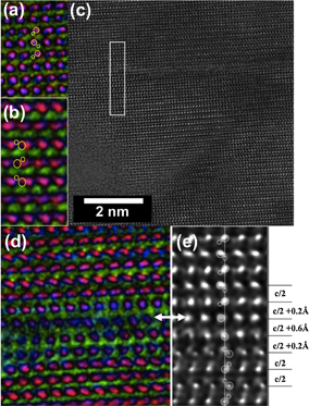
Fig. 19. High-resolution image of the part of the inversion domain observed in the GaN platelet. (a) Atomic arrangement in the matrix above the pyramidal interface [the area from the top of the rectangular box marked in (c)]. This area shows the matrix with Ga-growth polarity. Larger circles indicate Ga atoms and smaller N atoms. (b) Atomic arrangement in the domain below the interface (the lower part in the rectangular) indicating N-growth polarity within the domain. (c) High resolution image taken in [1120] projection of the right part corner of the pyramidal inversion domain. The rectangular box outlines the area from which all surrounding micrographs [(a, b) and (d, e)] are taken and shown in higher magnification. Note also that the area above the scale bar in this micrograph is much thinner in comparison to the right corner of the pyramid, indicating presence of a void in this area. (d) High resolution image from the pyramid/matrix interface (the center part in the box) shown in color. The color assignment is based on the Argant plot (discussed in detail in the Ref. 82). (e) Black/white contrast image from the same interfacial area with indicated distances between Ga–Ga rows of atoms across the ID/matrix interface. Note expansion of the Ga–Ga distances close to the interface terminating this domain, suggesting increased Mg accumulation close to the interface. Also it is worth noticing that it was impossible to assign the heavier and lighter atoms in the dumbbells at this interface and two rows with larger "blobs" are present, one at the interface and also one row below, suggesting two Mg atoms paired together in these two rows. The double arrow indicates the position of the inversion boundary terminating the inversion domain.
Download figure:
Standard image High-resolution image7.2. Models explaining Mg rich inversion domains
Liliental-Weber et al.73) proposed two possible models for the inversion domains formed on c-plane in GaN:Mg samples: one required Mg to be four-fold coordinated and the second model required Mg to be six-fold coordinated, similar to what was observed in AlN:O.84) Van de Walle and Neugebauer85) and Hansen et al.86) suggested that these inversion domains are Mg3N2 inclusions. Vennegues et al.87) confirmed earlier findings by Liliental-Weber et al.58,73–75,78) that these defects are inversion domains and suggested a different lattice occupancy on the perimeter of this defect due to the presence of Mg. These authors87) suggested the formation of Mg3N2 on the base and side-walls of this defect and claimed that "two N tetrahedra filled with Mg (filling factor 3/4) replace two N tetrahedra with only one filled with Ga, therefore the crystal charge neutrality is maintained".87) According to Vennegues et al. model87) the presence of Mg3N2 on the pyramidal border should not change the N sublattice across the side matrix/pyramid boundary and only Ga sublattice should be affected. However, Romano et al.77) also suggested the formation of Mg3N2 on the pyramidal border but claimed that Ga sublattice continues across the pyramidal inversion domain. Northrup88) calculated several models of the inversion domain boundary formed on (0001) plane including these proposed earlier by Liliental-Weber et al.,75) Venneagues et al.,87) Leroux et al.,79) and earlier proposed by Holt.89) This author88) suggested that at the boundary the "aabbaabb" sequence of atomic planes in GaN is substituted by the "abcab" equivalent to GaNMgNGa and Mg is placed on c-site. The author claimed that this "abcab" structure has the lowest energy among all calculated boundaries and considered that Mg occupies only 3/4 of possible c-sites and each Mg atom has six N neighbors at a distance of 2.33 Å.
However, one needs to consider that the inversion boundary formed on (0001) plane terminates the pyramid but these pyramids start to grow from the triangular tip. Therefore, suitable model needs to be developed explaining the formation of the polarity inversion starting at the tip and the side-walls from which the pyramid is growing and finally leads to the termination by the boundary on the (0001) plane. Such model needs to be consistent with the experimental data. Later studies by Liliental-Weber et al.81) showed clearly that Mg floats to the surface, confirmed also by Benzarti et al.90) Liliental-Weber et al.81) showed that Mg clusters are formed and these clusters are most probably the origin to the formation of pyramids and truncated pyramids. These authors showed that AB stacking of Ga–N present in the matrix below the pyramid change to the BC stacking of N–Ga within the pyramid and this is illustrated in Fig. 19. The same c/2 distance (c here is a lattice parameter) was measured inside and outside the pyramid. This definitely excludes the formation of Mg3N2 precipitates, as earlier suggested by some investigators.85,86) This BC stacking holds through the entire pyramid and changes to the AB stacking above the pyramid. Liliental-Weber et al.81) using the phase contrast measured the distance between Ga sublattices within the pyramid and across its base. The observation by these authors showed that c/2 distance expands on three consecutive planes below and one above the pyramidal inversion boundary, as shown in Fig. 19. The measured distance between Ga–Ga sublattice increases at least by 0.02 nm below and above the base. In some cases the expansion is observed on few monolayers by 0.02 nm followed by 0.06 nm below the base (within the pyramid) and by 0.02 nm above the base and then the distance between Ga–Ga sublattice immediately returns back to the c/2 distance above the pyramidal boundary, as measured for GaN matrix. This is consistent with Mg substituting Ga since the formation of Mg3N2, as previously suggested79) would give different interplanar distances. This expansion of the Ga–Ga distances would also suggest that Mg floats on the surface and its accumulation is larger on the areas with N growth polarity.
Liliental-Weber et al.80,81) also measured the interplanar distances along side-walls far enough from the border to avoid side-wall overlapping with the matrix. A distance of 0.06 ± 0.02 nm (equivalent to the distance between Ga and N along the c-axis) was measured between the Ga–Ga sublattices in the matrix and inside the pyramid, as schematically shown in Fig. 20. From these measurements it does not appear that there is any continuation of Ga or N sublattices across the side-walls, as suggested by other investigators.77,87) Liliental-Weber et al.81) explained decoration of side-walls by Mg leading to local inversion of growth polarity. These authors noticed that the {1123} planes in GaN (sides of the pyramidal inversion domains) consist of the same occupancy of Ga and N-sites and suggested that Mg might be situated equally (or similarly) on both sites and that most probably Mg occupancy on these sites is much lower than 100%. These authors81) also suggested that some positions might be taken by oxygen since oxygen was detected on the pyramidal side-walls and the base. Since Mg floats on the sample surface, confirmed by Benzarti et al.,90) then Mg can substitute both Ga and N sites. Two Mg atoms can be locally next to each other along the c-axis, as shown schematically in Fig. 20, and lead to local inversion of growth polarity. When growth proceeds a pyramid would grow to larger size but the growth rate with N polarity would be slower compared to the matrix grown with Ga polarity.
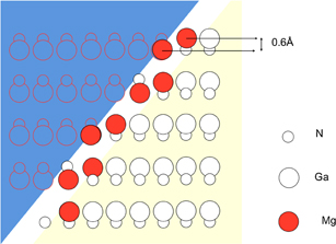
Fig. 20. A model of the inversion domain (left side represents the ID and right side the matrix) formed on the side of the pyramid with the matrix in [1100] projection. Red circles at the side boundary indicate possible positions of Mg atoms. It is assumed that only some positions are occupied by Mg and the remaining positions by Ga and possibly also by oxygen. However, it is possible that two Mg atoms in the vertical positions can be next to each other and can be responsible for the creation of the inversion.
Download figure:
Standard image High-resolution imageAnalysis of the reconstructed exit wave phase image displayed as Argant plot presented by Liliental-Weber et al.80,81) showed much stronger atom intensity on the base of the pyramid. As is shown in Figs. 19(d) and 19(e) instead of pair of atoms with lower and higher atomic number Z (N–Ga), as one can see below the base and Ga–N in the matrix, only one row of "dumbbells" with much stronger intensity is observed at the pyramid/matrix interface. Also smaller phase on the defect base, as seen in color in Fig. 19(d) is consistent with Mg substituting Ga and higher intensity of this row of "blobs" shown in Fig. 19(e) is consistent with the presence of a pair of Mg atoms in the base.
A single row of "blobs" with higher intensity was not observed on the sidewalls of the pyramids due to the fact that the high resolution imaging of pyramids was taken in [1120] projection, where the pyramidal sidewalls overlap with the matrix. However, the shift of about 0.06 nm between the Ga atomic row in the matrix and the Ga atomic row inside the pyramid is consistent with the presence of a pair of Mg atoms at the side-wall of the pyramid leading to polarity inversion. Since Mg occupancy on the side-wall border is not 100%, therefore local lack of Mg sometime would be expected (also disturbed by the presence of oxygen). In such circumstances a pyramid growth would be terminated and it would be overgrown by the matrix with its atomic sequence, as is shown in Figs. 19(a) and 19(b). This is also consistent with the fact that the growth rate of matrix along a-direction is faster than along c-direction. This is proven by the shape of the platelet crystals, where much larger length along the a-axis is measured in comparison with its thickness. When the pyramid is terminated the atomic sequence above the pyramid base will be exactly the same as in the matrix. This was always observed for any pyramid, independently on the pyramid size.
Understanding of Mg location on the pyramidal defects is very important in order to explain why an increase of Mg concentration above (2–6) × 1019 cm−3 leads to p saturation and a further increase of Mg concentration even results in a decrease of hole concentration.71,91) Venneagues et al.87) tried to relate the decrease of p-conductivity to the presence of the pyramidal inversion domains, especially that the number of pyramids increased with Mg concentration. Based on their model of Mg occupancy on the perimeters of the pyramids and taking into account pyramid density, these authors calculated the number of Mg atoms that need to be subtracted from the total number of Mg in the sample and showed that these inverted pyramids may account for the self-compensation phenomenon in Mg doped GaN.
7.3. Defects in Mg doped GaN layers grown by HNPS-MFS
Defects formed in Mg doped GaN layers grown by HNPS with the MFS configuration show rectangular precipitates, shown in Fig. 21 that decorate the dislocations propagating from HVPE GaN substrates. Studies by Liliental-Weber et al.68) and earlier studies of Smalc-Koziorowska92) showed the formation of the MgO precipitates that have a crystallographic orientation relationship of [0001]GaN ∥ [111]MgO. Some other inclusions can be also found in the Mg doped layers. These precipitates showed different thinning rate than the surrounding matrix during ion-milling and appeared to be amorphous but their chemical composition was not identified. They might contain oxygen since earlier SIMS studies of these layers show comparable concentration of oxygen and Mg. These layers appeared to be semi-insulating with the estimated resistivity of 1015–1016 Ω cm for crystals grown at 1420–1450 °C.17,93) Pyramidal inversion domains found earlier in high-pressure platelets were not found in these layers.

Fig. 21. MgO precipitates decorating a dislocation in the HNPS layer doped by Mg.
Download figure:
Standard image High-resolution image
8. Conclusions
This review shows that different type of defects can be formed in wurtzite GaN. Advances in the resolution of TEM techniques allow us to study these defects on atomic level and understand how they are formed. This information is essential to help the crystal growers to improve the growth process to eliminate these defects in order to use this material in future devices. Substantial progress in the growth of thin film and bulk GaN crystals was already achieved and will further lead to the elimination of these defects necessary for the improvement of performance for long working time of lasers, detectors and other devices.
Acknowledgments
This work was supported by the Director, Office of Science, Office of Basic Energy Sciences, Division of Materials Sciences and Engineering of the U.S. Department of Energy under Contract No. DE-AC02-05CH11231. The author is very indebted to Dr. K. M. Yu for careful reading and correcting of this manuscript and Dr. R. dos Reis for his help for the final preparation of the numerous figures to meet the requirement of the editor.
Biographies

Zuzanna Liliental-Weber was born in Poland. She graduated with a M.S. in Physics from Warsaw University, Poland and a Ph. D. in Solid State Physics in 1978 from the Institute of Physics Polish Academy of Sciences. She has spent more than 4 years (1980–1984) as Faculty Research Associate in Arizona State University, Tempe, AZ working on dark line defects in GaAs/AlGaAs light emitting diodes and interface roughness using different electron microscopy methods. Starting in 1984 she has been working in LBNL and since 1994 she worked as a senior staff scientist and a principal investigator in the Electronic Materials program in the Materials Sciences Division till her recent retirement in 2013. She continues her research as the LBNL affiliate. Dr. Liliental-Weber's work covers the area of structural defects in III–V semiconductor thin films and interfaces using state of the art transmission electron microscopy correlating the influence of these defects on the optical and electrical properties of the materials. Her interest includes p-doping, non-stoichiometry of semiconductor alloys and highly mismatched compound semiconductors. Her recent work on the effects of structural defects on cathodo- and photo-luminescence in the InGa1−N was featured in the covers of Physica Status Solidi. Her understanding of defect formation lead to the application of specific defects for stress relaxation at the GaN and Si substrate interface. This method of defect induced improvement of structural perfection of the GaN layers was granted a US patent in 2011. Dr. Liliental-Weber has published more than 500 papers in refereed journals and conference proceedings, review articles and book chapters.