Abstract
In the present article, we focus our discussion on the carrier dynamics of the scattering and recombination processes of InN films and the related band-edge energy structure. Various reports on this matter are summarized and some issues are reexamined. The analysis result based on the apparent band–band transition matrix element is consistent with a reported effective heavy hole mass of 0.59 (±0.06) m0. An Ep value related to the transition matrix element of 10–14 eV is thought to be plausible. The ambiguity of the band-edge structure is evaluated by the uncertainty of electron density. The distortion of the conduction band bottom and the ambiguity of the estimation of the many-body effect are discussed. The enhancement of the anisotropic electron-scattering nature with the decrease in residual electron density reveals that the residual electron source has isotropic potentials: point defects or small complexes. Infrared reflectance spectrum analysis reveals the high electron mobility inside grains in spite of the scattering by edge-type dislocations which cause the anisotropic carrier scattering. The recombination processes at low temperatures are dominated by nonradiative processes related to edge-type dislocations, while the thermally activated nonradiative recombination process is independent of the dislocation density. The activation processes and energies of the recombination related to phonon localization are characterized. InN is a peculiar material that has high carrier mobility and a strong electron–phonon interaction, which possibly induces the high nonradiative carrier recombination rate. The control of phonon localization is thus required.
Export citation and abstract BibTeX RIS
1. Introduction
About a dozen years ago, when the origin of the electronic transition in the absorption process was unclear, the fundamental optical absorption energy of InN was found to be less than 1 eV.1–4) After the discovery that the fundamental energy gap Eg was less than 0.65 eV at room temperature (RT),5–8) various studies were conducted on effective electron and hole masses, residual electron sources, surface electron accumulation, p-type doping and conductivity, the carrier-scattering mechanism, luminescence properties, and so forth. Currently applications in electronic and optical devices are being investigated.9–11) In this article, the physical properties of InN are reexamined on the basis of recent progress and, in particular, we focus on the carrier dynamics of the electron- and hole-scattering mechanism, the electron–hole recombination property, and especially the nonradiative recombination (NRR) processes. The energy structure around the electronic band edge is also examined as a basis of the discussion on carrier dynamics.
When Eg of less than 1 eV was proposed, discussion focused on the electronic transition process observed in the optical transmission and photoluminescence (PL) spectra. At this stage, the effect of the impurity band on the absorption spectra was not clear. As the electron density was reduced, smaller transition energies were reported. At present, the residual electron density has been reduced to the order of 1017 cm−3; however, the density at this order is greater than the Mott criterion, which is estimated to be approximately 1016 cm−3 in the case of an effective mass of 0.05m0. On the basis of the uniqueness of the transition matrix element for various residual electron densities in the range of 1 × 10¹⁹ to 2 × 1017 cm−3, Eg for the intrinsic material was confirmed to be approximately 0.63 eV at RT.6,7) Here, the electron density was obtained from infrared reflectance (IR) measurements. The effective electron mass has been discussed in many articles, and the value has been narrowed down to the range of 0.035m0–0.09m0,12–18) that is to say, the mean distance between two donors is smaller than the diameter of an electron wavefunction. These values were obtained by various analyses based on the dependence of Eg on the carrier density, coherent phonon measurements, IR measurements, and Landau levels in a magnetic field. The variation in the reported values was independent of analysis method. Rather, it appears that the variation is caused by the variation of the sample quality. It was also found that the donor level is located at a higher energy level than the conduction band minimum;19,20) thus, the ionized donors are thought to act as carrier-scattering centers even at low temperatures. In Sect. 2, the band-edge energy structure and the influence of defects are reexamined using the recent result for the valence band structure.
With regard to the carrier-scattering processes, researchers' interest has been focused on dislocations as another major carrier scattering source. We review and discuss the mechanism of carrier-scattering by threading dislocations and by point defects in Sect. 3. It is known that InN films have a surface electron accumulation region with an electron density of 1013 cm−2, and the electronic structure around the surface has been clarified.21–23) When electric detection methods such as Hall measurement were adopted, the dependence of the carrier density or conductivity on the film thickness was investigated because of the surface electron accumulation. The variable magnetic field revealed the mobility spectrum without the need to determine the film thickness dependence;24) however, the spatial resolution of the current path in a film could not be obtained by this analysis. On the other hand, IR reflectance (IRR) spectra provided information on the depth profile of plasmon properties, because of the dispersion of the dielectric function around the LO phonon and plasmon energy region, and therefore information on the dependence of the penetration depth on the wavelength of the incident light.25) Furthermore, the control of the light polarization enabled us to detect the anisotropy of the carrier dynamics. Thus, IRR analysis has been used as a noncontact and nondestructive approach to carrier property characterization for various materials. For InN the electron density and scattering rate in the bulk region, excluding at the surface and interface, have been discussed.25–28) Since the generation of net acceptors in Mg-doped InN films was achieved,29–31) hole properties have been investigated. In Hall measurements the condition of a quarter period of cyclotron motion before scattering gives the relation σB = π/2, where B and σ are the applied magnetic field and carrier mobility, respectively. When we take the criterion for the resolution of carrier mobility of σB = 0.1, then a magnetic field of 10 T is required for the detection of a mobility of 100 cm2 V−1 s−1. In particular, for the analysis of hole mobility on the order of 10 cm2 V−1 s−1, a high magnetic field of 10–100 T is desired. In Raman measurements, no peaks have been observed at the higher branch energy level of the LO phonon–plasmon coupling (LOPC+) mode that was observed by IRR for both n- and p-type samples. The reason for this has been investigated in conjunction with the high carrier scattering rate by several groups, whose works are cited in this article.32) In particular for p-InN, the high scattering rate of holes is also reflected in the small energy shift of the LOPC+ mode from the LO mode in IRR, which is discussed in Sect. 3.
From the viewpoint of the application of InN to IR light emitting devices, the radiation efficiency and dominant physical process in the NRR of carriers have been discussed for n- and p-type samples. Generally the NRR rate is determined by the density of recombination centers, the rate of carrier transport to the centers, and the activation probability or cross section of the NRR processes. The energy structure of the defect–carrier system has been discussed using a configuration coordinate (CC) diagram.33–35) The activation processes of NRR are discussed using this scheme. With regard to the two properties of carrier transport and NRR activation, InN has particular properties never observed in other III–V materials. The difference between the inverse values of the dielectric constants at the infinite and low frequency limits is about two or three times the value for typical III–V materials, which means that InN has strong electron lattice coupling, and thus there is a high activation probability for NRR processes in the lattice vibration field, which is shown in Sect. 4. The smaller effective electron and hole masses than GaN and AlN and greater carrier mobility mean a high transport rate of minority carriers to the NRR centers in n- and p-type films. On the basis of these results, the peculiar properties of InN in NRR processes are reported. The samples discussed in this article have the C-face surfaces. The samples with a +C-face have a lower residual electron density on the order of 1017 cm−3, while the samples with a −C-face have a density of 1018 cm−3 or more. The edge type and screw-type dislocation densities are (0.94–3.2) × 1010 and (1.7–7.9) × 108 cm−2, respectively.
2. Fundamental electronic properties around the Γ point
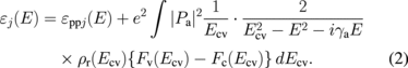
In the analysis of Eg, the spectra of the absorption coefficient α or the product of the squares of α and the photon energy E, α2E2, have been investigated. Since the lowest residual electron density in the present study on InN, on the order of 1017 cm−3, is greater than the Mott transition criterion, which is a density of 1 × 1016 cm−3 in the case of me = 0.05m0, the exciton effect is neglected. Since InN is an optically direct transition-type material, the absorption coefficient due to the valence band to conduction band transition is formulated by Eq. (1),36) and thus α2E2 becomes a linear function of E when the transition energy is expressed as a parabolic function of the wavevector

where ρr(E) is the joint density of states and FV(E) and FC(E) are the quasi-Fermi functions of the electrons and holes, respectively, at temperature T in the joint valence and conduction band system. FV(E) and FC(E) are expressed using the effective electron mass me, effective hole mass mh, reduced effective mass  , and quasi-Fermi levels of the electron μc, and hole μv (see Appendix A). Equation (1) includes the dependence of the refractive index on the transition energy E. On the other hand, Ishitani et al. analyzed multiple reflectances in samples using the transfer matrix method based on the following dielectric function, which is obtained from the quantum mechanical expression for the density current37)
The vibration direction is denoted by j, while εppj(E) is the component of the phonon and plasmon term that is shown in Appendix B. The second electronic term was assumed to be isotropic. Figure 1 shows examples of the PL and  spectra. Here, αa is the effective absorption coefficient, defined as αa = ln Tr/d, where Tr and d are the transmittance and film thickness, respectively. The wavelength of the excitation laser is 0.98 µm. All the PL spectra in this report were obtained using the same excitation wavelength. In the analysis of the band-edge energy structure, the non-parabolic energy structure of the conduction band bottom and the many body effect originating from the degenerated conduction band bottom were taken into account. A parameter Ep, defined as 2|〈S|px|X〉|2/m0 = 2m0|P|2/ħ2, is usually used in the formula for the conduction band energy structure of the non-parabolic function of the electron wavevector ke.3,38) The effective electron mass at the conduction band bottom has been discussed on the basis of the expression of
  , while the many-body effect consists of two terms concerning the Hartree–Fock exchange interaction and the ion-electron interaction.4,5,7,14,39,40) |Pa| is the effective transition matrix element.

Fig. 1. PL and  spectra at 14 K for three
  of A: 8.4 × 1018 cm−3, B: 6.0 × 1019 cm−3, and C: 1.8 × 1020 cm−3. The solid curves represent the theoretical function using Eq. (2):
  and Eq. (A·9): PL. The dotted curve for sample A is calculated for the temperature of 14 K.
Download figure:
Standard image High-resolution imageIshitani and co-workers analyzed the transition matrix element to determine whether |Pa|2 varies with an increase in the residual electron density, and they found that |Pa|2 was constant.7,14) Here, the discussion will be extended to the consistency of the magnitude of the absorption coefficient and the band-edge energy structures of the valence band, and the non-parabolic conduction band is shown on the basis of the spectrum fitting of  and the PL spectra, where Eg, the chemical potential μc, and the broadening of the transition energy γa are adjusted. Since the dielectric function obtained by spectroscopic ellipsometry has an almost constant real part at approximately 1.5 eV,41,42) the critical points with higher energy have minimal effect on the electronic energy structure near the Γ point below 1 eV.
Initially, we will focus on the absorption edge energy, which is the sum of Eg and μc. Figure 2(a) shows examples of s-polarized IRR spectra at RT. The experimental IRR spectra were analyzed by the transfer matrix method based on multilayer models. The model dielectric function consists of a phonon–plasmon term and an electronic transition term [Eq. (2), Appendices A and B].25,27) As a result, the electron density inside the bulk region except for at the surface and interface accumulation layers was obtained. The detail of the fitting is described in Sect. 3. The solid curves are the best-fit functions. The film thickness and  were obtained from the spectrum analysis. The adjusted spectra fit the experimental results in the whole energy range. As shown by the arrows in this figure, LOPC energies appear as the spectrum edge energies,27) while these energies are clearly shown to be spectrum peak positions in the imaginary part of the inverse of the pseudo-dielectric function obtained by IR ellipsometry as shown in Fig. 2(b).
  is determined from the spectrum edges of the LOPC modes. Table I shows the adjusted band parameters by the analysis of
  or IRR. Figure 3 gives a summary of the relationship between
  for the bulk region and the absorption edge energy obtained from
  or reflectance spectra. The experimental plots were calibrated for the residual strain. The curves are the theoretical functions calculated by taking account of the non-parabolic conduction band energy structure based on k · p perturbation theory and the many-body effect. The band renormalization factor (ΔEr) was calculated in accordance with Refs. 4 and 40, and as an example, was found to be 31 meV for sample A. The parameters used in the calculation are listed in the inset. The strain effect ΔEs is calculated using the experimental results of the 2θ–ω X-ray diffraction pattern, deformation potentials, and elastic constants.43,44) We reexamine this variation of the absorption edge energy on the basis of hole effective mass mh values that have been recently reported. Effective hole masses mh (
 ) showing total DOS (Appendix A) of 0.74 m0 and 2.4 m0 were examined. These two values respectively correspond to the effective heavy hole mass mhh with the isotropic value of 0.59 m045) and the anisotropic values of 1.69 m0 (⊥c) and 2.0 m0 (∥c).46) The functions in the range of Ep from 10 to 18 eV fit the experimental plots for
  smaller than 1.5 × 1019 cm−3, however, there is a large discrepancy between the experimental data and the theoretical function in the larger
  region. The curve for Ep = 10 eV and
  agrees with the experimental spectra in the larger-energy region and deviates from the experimental plots in the smaller-
 region. We will now discuss possible origins of this discrepancy. The anisotropy of the conduction band bottom structure11,12) is too small to explain this result, and the relaxation of the k-selection rule is also a minor factor since the observed PL peak energy of 0.7 eV for sample C is smaller than the absorption edge energy of 0.84 eV. The difference in the chemical potential by experimental analysis of the experimental
  spectra and the calculation based on
  from the IRR analysis is within approximately 30 meV for the example of Ep = 14 eV. This discrepancy in the chemical potential between the theory and the experiment corresponds to an uncertainty of 4–24% in
  . This uncertainty shows the ambiguity of the band edge energy structure from the viewpoint of electron density. This ambiguity is attributed to the modification of the band-edge energy structure by the strain field around crystal defects, the Coulomb field around charged defects, and so forth.

Download figure:
Standard image High-resolution image
Fig. 2. Examples of IRR spectra at RT (a) and the inverse of the imaginary part of the pseudo-dielectric function (b). The incidence angle is 30°. The obtained values of  are noted in the figure. The absorption edge positions and LOPC± positions are indicated by arrows. The inset of (a) shows the spectrum of a sapphire substrate. The sample structure is an InN film on a sapphire substrate for the samples with
  and 3.7 × 1019 cm−3 and an InN film on a GaN layer grown on a sapphire substrate for the other two samples in (a). The InN film thickness is 4–5 µm.
Download figure:
Standard image High-resolution image
Fig. 3. Absorption edge energy plotted as a function of  at 14–16 K. The closed circles are the experimental plots. The energies were compensated for the strain effect. The curves show the result of the theoretical calculation based on the parameters listed in the figure. The energy gap shrinkage due to the many-body effect is taken into account in the calculation.
Download figure:
Standard image High-resolution imageTable I. Adjusted parameters in the dielectric function. The experimental methods used to obtain the parameters are noted below the parameter symbols. The chemical potential μc is obtained from  by IRR and the theoretical density of states using Ep = 14, 10, and 8 eV. A parabolic valence band structure with
  is assumed. ΔEr is calculated using a formula given in Ref. 40. ΔEs is calculated using the 2θ–ω X-ray diffraction pattern. The |Pa|2/|P|2 values are for Ep = 14 eV.
| Sample |  (1018 cm−3) (IRR) (1018 cm−3) (IRR) |
μc (eV) (theory) | Eg (eV) μc (eV)  |
ΔEr + ΔEs (meV) | |Pa|2/|P|2 ( Ry) Ry)  |
Eg (eV) μc (eV) (PL) |
|---|---|---|---|---|---|---|
| 0.041 | ||||||
| A | 8(±1) | 0.037 | 0.636 | 14 | 1.2 | 0.662 |
| 0.034 | 0.055 | 0.025 | ||||
| 0.163 | ||||||
| B | 6.0 × 10 | 0.145 | 0.605 | 54 | 1.2 | 0.652 |
| 0.135 | 0.132 | 0.035 | ||||
| 0.341 | ||||||
| C | 1.8 × 10² | 0.305 | 0.520 | 123 | 1.0 | 0.658 |
| 0.284 | 0.330 | 0.048 | ||||
| 0.057 | ||||||
| D | 1.3 × 10 | 0.051 | 0.641 | 14 | 1.3 | 0.657 |
| 0.048 | 0.057 | 0.031 | ||||
| 0.026 | ||||||
| E | 4 (±0.5) | 0.024 | 0.662 | 12 | 1.2 | 0.653 |
| 0.024 | 0.024 | 0.024 | ||||
The theoretical |Pa|2/|P|2 obtained using the simplified band model similar to that for GaN shown in Appendix A is 1.13, which is in agreement with the experimental results for  as shown in Table I. This value of slightly greater than unity is due to the contribution of three valence bands or the multiplet angular momentum states at the Γ point of the valence bands. However, in the case of
  , it was found that the experimental |Pa|2/|P|2 values for Ep of 8, 10, and 14 eV are 0.93, 0.97, and 1.0, respectively, where the uncertainly of |Pa|2/|P|2 is 2%. All of these values are less than or equal to unity. Thus, this
  disagrees with the optical transmission spectrum feature. For
  of 0.59, the |Pa|2/|P|2 value decreases from 1.2–1.1 as Ep decreases from 14 to 8 eV. The chemical potential μc was found to decrease by nearly 10 meV when Ep decreases from 14 to 8 eV for samples A and D. It was found that |Pa|2/|P|2 is almost constant even though ne increases. Although Fig. 3 shows that Ep in the range of 10–18 eV is possible, |Pa|2/|P|2 analysis reveals that 10–14 eV is plausible.
Figure 4 shows examples of the dependence of the PL peak energy, emission efficiency, and peak width on the excitation power for sample E.47) The measurement temperature was 15 K. When the excitation power is increased, the carrier transition process shifts from one via the shallow localization level to band–band recombination, and thus the full width at half maximum (FWHM) decreases. Under a high-excitation condition, we find a gradual increase and a tendency towards saturation of the PL peak energy and a decrease in PL efficiency. This result indicates that an increase in excitation power induces NRR processes, which possibly increase the electron temperature.

Download figure:
Standard image High-resolution image
Fig. 4. Dependence of PL spectrum properties on excitation power for a sample with  cm−3; peak energy and luminescence efficiency IPL/Iex (a) and FWHM of the peak (b).
Download figure:
Standard image High-resolution imageThe Eg and μc obtained by fitting the PL spectrum disagree with the results of the transmission spectra. Figure 1 shows that the PL spectrum edge positions on the lower-energy side, which are indicated by the fitted function drawn as the solid curve, are approximately 0.65 eV for all samples. Thus, the spectra do not reflect the decrease in Eg, although a decrease in Eg with increasing ne was found in the  analysis as shown in Table I. Furthermore, the temperatures of the best fit of PL spectra (solid curves in Fig. 1) were 35–90 K. For larger
  , a higher temperature was obtained. In the analytical formula given by Eq. (A·9), the nonuniformity of Eg in the film was not taken into account. The broadening of the spectra and the high carrier temperature in the fitting are possibly due to the non-uniformity of Eg and the electron density in the films. Thus, the actual carrier temperature is unknown.
Therefore, a probable origin of the discrepancy in Fig. 3 is the uncertainty of the bandgap shrinkage due to the many-body effect. Another probable origin is the distortion of the conduction band structure due to defects. It is recommended that physical properties such as effective mass are examined by considering transmission spectra, in particular, using samples with ne on the order of 1017 cm−3. Additional electronic states around the conduction band were reported by Inushima et al.48) and Dmowski et al.49) Since the distortion of the bands is limited to the lower energy levels for the samples with low electron density, most of the region in an absorption spectrum is free from distortion.
The energy splitting of the valence bands of  (heavy hole)–
 (spin–orbit split hole): 3 meV and
  –
– (crystal-field split hole): 21 meV was obtained by ellipsometry analysis.50) It has been reported that
  is located at a higher energy than
  and
and  ;36,51,52) however, it appears that additional discussion of the energy position of these two levels is required. Figure 5 shows examples of polarized PL spectra obtained using polarized PL analysis. The excitation laser light was incident on the cleaved edge perpendicular to the c-axis. From the analogy of the selection rule for GaN, the π light luminescence with the electric field parallel to the c-axis originates from the
  –
– transition, and the σ light luminescence with the electric field vertical to the c-axis originates from the
  –
– and
and  –
– transitions. The sample in Fig. 5(a) (
 cm−3) shows that
  –
– or
or  –
– is the main transition process, while for the sample in Fig. 5(b) (
 cm−3)
cm−3)  –
– is the main transition process at 18 K. Furthermore, Fig. 5(b) shows that the main transition process changes from
  –
– or
or  –
– to
to  –
– as the temperature decreases. This result indicates that
  ,
,  , and
, and  are closely positioned and that small changes in the strain field modify the relative positions of the valence band maxima. The highest valence band state is possibly changed by some extrinsic effects of strain, defects, and so forth. The intrinsic valence band structure should be investigated using samples with a lower defect density. Thus, an unknown factor remains in determining the band-edge energy structure.

Download figure:
Standard image High-resolution image
Fig. 5. Polarized PL spectra for two samples with  cm−3 (a) and
  cm−3 (b). The laser light is incident on the cleaved edge of the sample from the direction perpendicular to the c-axis. The polarization direction of the π light is parallel to the c-axis and that of the σ light is perpendicular to the c-axis. The excitation laser is σ-polarized.
Download figure:
Standard image High-resolution imageThe energy structure of InN has been investigated in many theoretical studies and one notable reference is cited here. Obata et al. proposed that the interaction of the second nearest In–In atoms is effective for InN with small Eg and also for determining the electric conductance in a film with a high density of VN vacancies.53)
Figure 6 shows the dependence of the transition energy (Eg + μc) on temperature. This was obtained from the absorption spectrum analysis. The temperature dependence of Eg has been reported in several papers.5,6) The difference between the transition energy at 14 and 300 K is approximately 45 meV. The chemical potential μc was assumed to be constant in this temperature range. The dependence of Eg on temperature is expressed by the following equation;


Here αv(T), (∂Ecv/∂P)T, and V(∂P/∂V)T are the volume-thermal expansion coefficient, deformation potential, and bulk modulus, respectively. Ev(T) represents the shrinkage of the energy gap with increasing thermal volume. These parameters were assigned the values in Refs. 4, 44, and 45 of (∂Ecv/∂P)T = 1.8–3.3 meV/kbar and V(∂P/∂V)T = 1260–1480 kbar. These two values are assumed to be independent of temperature. The dependence of αv(T) was obtained from the interpolation of reference data for 2α⊥(T) + α∥(T), where α⊥(T) and α∥(T) are the linear thermal expansion coefficient in the directions perpendicular and parallel to the c-axis, respectively,44) and the extrapolation to temperatures lower than 50 K was based on the T3 law in the low-temperature range. As a result of the least-squares fitting, E0, ED, and θD were obtained as 0.719–723 eV, 0.027–0.035 eV, and 188–198 K, respectively, in the reference range of (∂Ecv/∂P)T and V(∂P/∂V)T. The uncertainties of E0, ED, and θD were 3 meV, 7 meV, and 35 K, respectively. The solid curve in Fig. 6 is the best-fit function for (∂Ecv/∂P)T = 3.3 meV/kbar and V(∂P/∂V)T = 1480 kbar. The author has investigated the parameters of GaxIn1−xP crystals (x = 0, 0.52, 0.70, 1.0, Eg at the Γ point at 12 K: 1.41, 2.0, 2.26, 2.87 eV) by taking account of Ev(T). ED for InN is smaller than the values of 0.07–0.11 eV for the GaxIn1−xP system.54) The Debye temperature θD was also smaller than the values for the GaxIn1−xP system of 200–250 K. The formula for Eg as a function of temperature consists of a self-energy term and Debye–Waller term.55,56) These two terms have opposite signs, and are contributed to by the intra band and interband perturbation terms, respectively, which also have opposite signs. Although the dependence of Eg on temperature is thus complicated, III–nitrides have a smaller variation of Eg with temperature than other III–V compounds.

Fig. 6. Dependence of transition energy on temperature for a sample with  cm−3. The solid curve is the best-fit function using (∂Ecv/∂P)T = 3.3 meV/kbar and V(∂P/∂V)T = 1480 kbar. The dashed curve shows 0.705 eV − Ev(T). E0, ED, and θD were obtained as 0.719 (±0.003) eV, 0.027 (±0.007) eV, and 188 (±35) K, respectively.
Download figure:
Standard image High-resolution image3. Carrier-scattering properties
In the IRR spectrum fitting, electron accumulation layers were taken into account. Figure 7 shows the IRR spectra of sample E in the LOPC− energy range. This figure indicates that layer structure models with an electron accumulation layer at the interface with the substrate reproduce the experimental spectra, while the spectrum based on the model without the electron accumulation layer deviates from the experimental data. In Ref. 25 the depth profile of the electron density was discussed, and the value inside the bulk region except for at the surface and the interface with the substrate was obtained. Here the contribution of the surface accumulation was found to be negligible in the IRR spectra. A possible reason for the nondetection of surface electron accumulation in IRR is the negligible response of the electrons in the accumulation layer to the electric field modulation in the THz region. The measurements down to the LOPC− energy region enabled us to analyze the accumulation layers using samples with ne on the order of 1017 cm−3. This is because the incident light in the LOPC− region penetrates to the film-substrate interface region, which enables us to discriminate between the accumulations of the interface and surface.

Fig. 7. Infrared reflectance spectra of the sample with  cm−3 in the LOPC− energy region. The solid curve is the best-fit curve to a model including an electron accumulation layer at the interface with the substrate (GaN/sapphire). The dashed curve is based on a model without an electron accumulation layer.
Download figure:
Standard image High-resolution imageFigure 8(a) shows the rate of electron-plasmon scattering for the vibration perpendicular to the c-axis obtained from the broadening factor γp⊥ via IRR analysis.26) The minimum γp⊥ in Ref. 57 was 38 cm−1 a scattering time of 140 fs, which corresponds to electron mobilities of 5300 cm2 V−1 s−1 for  and 2700 cm2 V−1 s−1 for
  . These values are greater than those obtained by analysis by Hall measurements, where values of up to 2150 cm2 V−1 s−1 were obtained for the samples investigated in Ref. 57. High values obtained by reflectance analysis were also reported by other groups.12,16) Inushima et al.16) reported γp⊥ of 3.3 meV (26 cm−1) for a conduction band with ne = 3 × 1017 cm−3, which corresponds to 4300 cm2 V−1 s−1 for
  . Chang et al. obtained a scattering time of the LOPC− mode of 200 ps for an electron density of 5 × 1017 cm−3 by performing the coherent phonon experiments.12) When the plasmon scattering time is approximated by that of the LOPC− mode for this electron density, this value corresponds to 3860 cm2 V−1 s−1 for
  and 7600 cm2 V−1 s−1 for
  . The reason that the values obtained by optical measurements are greater than those obtained by the Hall measurements is thought to be that the optical spectra mainly reflect the properties inside the grains rather than at the grain boundaries, which have a minor volume proportion.25) Multiple carrier properties were also detected by Hall measurements using a variable magnetic field;58) however, it is thought that obtaining the spatial resolution is beyond the scope of this analysis.

Download figure:
Standard image High-resolution image
Fig. 8. Carrier scattering properties of n-InN films at RT; (a) scattering rate of the plasmon vibrating perpendicular to the c-axis, (b) anisotropy of the scattering rate of the LOPC+ mode. In (a) the plots for N-polarity samples are denoted by N beside the symbols. The open circles in (b) are for samples with a larger edge-type dislocation density of 2 × 1010 cm−2.
Download figure:
Standard image High-resolution imageAlthough the data points in Fig. 8(a) are scattered, the minimum line for every carrier density increases with electron density. Among the investigated samples, the N-polarity samples have a larger carrier density on the order of 1018 cm−3 or more, while the In-polarity samples have a carrier-density of (1–2) × 1018 cm−3 or less. For γp⊥ the In-polarity samples have greater values than the N-polarity ones. However, γp⊥ tends to increase with  . The scattering potential structure was also studied by polarized reflectance analysis. The electron scattering by charged threading dislocations, which are edge type dislocations, was discussed by several groups.59–61) An increase in the electron mobility with a decrease in the threading dislocation density was found.59,60) However, it is probable that various kinds of defects including point defects were generated in the vicinity of the dislocations. Thus, the correlation is insufficient to specify the scattering sources. Miller et al. studied the two scattering components of charged dislocations and charged point defects by performing the measurements of the dependence of mobility and the Seebeck coefficient on temperature and theoretical analysis. They found that the electrons are mainly scattered by charged dislocations.61)
The advantage of polarized IR analysis becomes apparent in the study of the scattering anisotropy of carriers. Figure 8(b) shows the broadening anisotropy of the LOPC+ mode. P+ = (γ+∥ − γ+⊥)/γ+⊥ decreases with increasing in  . Here phonon–plasmon vibration perpendicular and parallel to the c-axis are denoted by ⊥ and ∥, respectively. P+ includes the phonon anisotropy and plasmon broadening anisotropy Pp of (γp∥ − γp⊥)/γp⊥. Pp was obtained for a few samples: it was approximately 3 for
  of 3.8 × 1018 cm−3 and 2 for
  of 3.8 × 1019 cm−3.26) The decrease in γp∥ with increasing ne agrees with the dependence of P+. P+ was found to be larger for samples with a larger edge type dislocation density. This anisotropy shown by P+ was attributed to the plasmon scattering anisotropy or scattering potential anisotropy rather than the anisotropy of the LO phonon scattering rate, the anisotropy of the electron mass, or the nonuniform ne.54) Also the enhancement of the anisotropy with increasing dislocation density is found in the lower-electron-density region as shown in Fig. 8(b). These results reveal that the density of defects with isotropic scattering potential decreases much more rapidly than the density of defects with anisotropic scattering potential as the electron density decreases. Therefore the dislocations were found to be the dominant scattering centers particular for the samples with low electron density. It was found that this phenomenon also holds for the holes in p-type samples.25) Since the density of the edge-type dislocations was approximately 3 × 1010 cm−2 or larger for the In-polarity samples (
 cm−3) investigated in the studies reported by Ishitani et al., the distance between dislocations was about 60 nm or less.26) The estimated Debye screening length was 10 nm at RT, which suggests that approximately 30% of electrons are contained in this potential field of charged lines. Since the energy level of the residual electron source is reported to be located above the conduction band minimum,19,20) almost all the defects generating electrons are ionized. Thus, if we assume that the main source of the residual electrons is edge-type dislocations, P+ or Pp would decrease with decreasing carrier density because of the decrease in the number of anisotropic charged lines, which is inconsistent with our experimental findings. The decrease in the density of point defects with isotropic potentials is in contrasted to the remaining of anisotropic scattering potentials shown by P+. Thus, the residual electron sources are thought to have isotropic potentials: point defects or complexes. Zhang et al. investigated the dependence of Hall mobility on temperature and analyzed the results by theoretical calculation based on the Brooks–Herring and Conwell–Weisskopf formulations.62) They reported that the scattering at the grain boundaries affects the electron mobility in N-polarity InN films, while it is negligible in In-polarity InN films. However, the grain boundary effect is minor in the IRR spectra,26) and the phenomenon observed by IRR is due to the matter inside grains.
Polyakov and Schwierz conducted a theoretical calculation based on the Brooks–Herring and Conwell–Weisskopf formulations and an electron mass dispersion curve with  at the conduction band bottom, and obtained a maximum mobility of 14000 cm2 V−1 s−1 at 32 kV/cm.63)
Since the theoretical calculation of the scattering rate is conducted using the Brooks–Herring and Conwell–Weisskopf formulations in many cases, we examine the validity of the Born approximation which is a basis of these formulations. The Born approximation, which is based on the first-order perturbation approximation, is valid when ka ≪ 1 or  is satisfied,64) where U and a are the perturbation potential energy and the spatial size of the potential field, respectively. The first condition, ka ≪ 1, is that a negligible quantum mechanical phase shift. The second one means that the potential energy is taken as a perturbation from the viewpoint of the quantum mechanical uncertainty principle. The first condition is transformed to
  in the unit of nm. When we take
  , a ≪ 24 nm for T = 10 K and a ≪ 4.3 nm for T = 300 K are obtained, while a is calculated to be 11 nm for ε(0) = 10.8 ε0. Thus the phase shift is not negligible. The second condition is transformed to U ≪ 120/a (meV). When we take a = 11 nm, we find that U ≪ 11 meV is required, while U is calculated to be 5 meV for ε(0) = 10.8 ε0. Thus, the potential energy cannot be taken as a perturbation. Therefore, the Born approximation is not valid for the present scattering process. For the precise estimation, a calculation based on the partial wave technique65) is required. This method enables us to obtain a precise phase shift by selecting a suitable cutoff wavenumber for the calculation of the scattering cross section.
Raman spectroscopy is also widely used in the study of carrier density and scattering processes. In the analysis of IRR and ellipsometry, the spectrum of −Im(1/ε) showed two peaks positioned at the LOPC− and LOPC+ energies.52,66) A typical spectrum is shown in Fig. 2(b). However, although a peak is observed around the LO phonon energy in a Raman spectrum, clear LOPC signals were weak or under the detection limit.17,67,68) Demangeot et al. proposed a model of phonon scattering with larger wavevectors than the Thomas-Fermi wavevector.67) They attributed this scattering causing the decoupling of LO phonons from plasmons to the charge density fluctuation of impurities. Inushima et al. proposed a mechanism based on the Fano type interference of LO phonons and the electronic continuum in the conduction band.17) When a phonon is decoupled from a plasmon by the scattering due to charge density fluctuation, Fano-type interference is thought to be possible.68) Davydov et al. reported the consistency between the energy dispersion curves of the phonon modes and the electronic energy bands in the double resonance scheme of Raman processes.69) Cho et al. demonstrated the transition of the Raman process from plasmon-related excitation to the double resonance process presented by Davydov.32) On the other hand, Cuscó et al. found that the energy of the weak signal peak located adjacent to the TO phonon peak agrees with the energy dispersion curve of the LOPC− mode.72) The Raman spectra for the present InN are complicated; however, they are sensitive to the carrier-scattering phenomena.
In this paragraph hole scattering properties are discussed. The existence of net acceptors was detected in several studies.29–31,69,70) Wang et al. obtained the hole conductivity from the dependence of the conductance on the film thickness, and the hole mobility was estimated to be in the range of 17–36 cm2 V−1 s−1.71) A Hall measurement using a variable magnetic field showed the contribution of hole conductivity.72) Measurement of the hole density and mobility using a single sample was performed by IRR analysis, where the dependence of the LOPC energy on the hole scattering rate was taken into account (Appendix B) since it is known that the LOPC mode energies are modified by the plasmon damping rate under an over-doped condition, which is described in Appendix B using Fig. A·2.25,45,73) Harima et al. found that there was no Raman peak corresponding to the LOPC+ mode energy, expressed by Eq. (B·2) in Appendix B for p-GaN.74) We have also found that the Raman spectra for p-InN also have no peak at the energy calculated using Eq. (B·2). In Ref. 73 it was found that the characteristic features of hole plasmon and LO phonon coupling were reflected in the IRR spectrum shape. Thus the spectrum fitting was conducted. In Refs. 73 and 45 the spectra at 5 K were analyzed while taking account of the terms of the phonon, plasmon, and the electronic transition between the valence band and acceptors. At RT the terms of the phonon and the hole plasmon were investigated. Figures 9(a) and 9(b) show the dependence of the carrier density on the doped Mg density [Mg] and the dependence of the hole-scattering rate γp⊥ on [Mg], respectively, measured at RT.45) Here three hole bands around the valence band maximum were taken into account. Although Raman peaks originating from the Mg–N–H bonding were reported, suggesting the inactivation of the Mg atoms as acceptors, such spectra were weak or below the detection limit of 2% of the E2(high) peak intensity for the present samples grown by MBE.45) For In-polarity samples, the hole density was mainly found to be on the order of 1016 or 1017 cm−3, and the maximum value was 2 × 1018 cm−3. The average cross section of the ionized impurity scattering and the neutral impurity scattering was obtained to be 3.1 × 10⁻¹⁴ cm2 (a Bohr radius of 0.99 nm) from the slope of the dependence shown in Fig. 9(b). This result means that the effective area of the scattering potential agrees with the size of a Mg atom calculated from the Bohr radius of a pair consisting of a hole and a Mg acceptor (0.97 nm). The intercept of the dependence in Fig. 9(b) is 6.0 × 10¹³ s−1, which is interpreted as the hole scattering rate of minority carriers at RT. The anisotropic weakening of the LO phonon and hole plasmon coupling by overdamping was investigated on the basis of the energy shift of the LOPC+ mode from the A1(LO) or E1(LO) mode measured by IR ellipsometry in Ref. 25. It was found that the energy of the observed vibration mode perpendicular to the c-axis shifted from the E1(LO) phonon energy by approximately 10 cm−1, while the mode parallel to the c-axis showed no energy shift from the A1(LO) mode. Thus, A1(LO) was more severely decoupled from the hole plasmon than the E1(LO) mode. The effective mass of the holes and the acceptor ionization energy were investigated in several studies. Figure 9(c) shows the dependence of the acceptor activation energy on [Mg] at 5–14 K. This dependence is attributed to the potential overlapping of ionized acceptors; thus, the activation energy decreases with increasing doped [Mg]. In the constant-activation-energy region, [Mg]+ is thought to be constant. This result is consistent with the following picture: when doped [Mg] is lower than the residual electron density, [Mg]+ in the film increases with doped [Mg], while in the higher-[Mg] region [Mg]+ and thus the activation energy are constant. An activation energy of 69 (±5) meV at the low-acceptor-density limit was obtained. Using this activation energy,  of 0.59 (±0.06) was obtained using a hydrogen-like energy model. In this analysis the acceptor ionization energy, hole density, and effective hole mass were obtained consistently, where the contribution of the three hole bands was taken into account but the energy splitting was neglected.45) In Sect. 2 this hole effective mass of 0.59m0 was utilized. In an analysis of Landau levels by PL measurements, a greater effective mass of 2.3–2.8m0 was reported.15) However, when
  is assumed, since the increase in mh from 0.5m0 to 2.5m0 causes the increase in the reduced mass of an electron and a hole pair by 8%, the reduced mass is insensitive to the hole mass in this range. In theoretical calculation, values of
  perpendicular to the c-axis of 1.69,75) 0.14,76) and 1.2677) were reported. When there is strong anisotropy for
  of 0.14 for ⊥c and 2.0 for ∥c, as indicated by Carrier and Wei,76) from a viewpoint of the DOS the average hole mass is 0.34, which is smaller than the experimental value of 0.59. In this case the carrier density obtained in Ref. 45 becomes 46%, which still leads to a maximum hole density on the order of 1018 cm−3 for N-polarity samples. Thus, a high hole density on the order of 1018 cm−3 is thought to be possible for InN, particularly for N-polarity films. Since the IR spectra reveal the value of
  , a larger effective mass results in a higher hole density and
  of more than 2m0 does not match the result of IR analysis.

Fig. 9. Hole and acceptor properties; (a) carrier density and mobility as a function of Mg doping density at RT for N-polarity samples, (b) scattering rate of holes vibrating perpendicular to the c-axis at RT, and (c) acceptor activation energy. The open circles and open squares in (b) indicate the data for In-polarity and N-polarity, respectively. The closed squares in (c) indicate N-polarity.
Download figure:
Standard image High-resolution image4. Luminescence intensity and nonradiative carrier recombination dynamics
From the viewpoint of the application of InN to IR light-emitting devices, electron and hole recombination processes have been studied by many groups. Klochikhin et al. analyzed the PL spectrum shape of n-type films and found two acceptor levels located at 5–10 meV and 50–55 meV above the valence band maximum.78) For the luminescence efficiency it was found that the emission of p-type samples was several orders of magnitude weaker than that of n-type samples or below the detection limit.29,79) So far, a wide range of PL lifetimes or carrier lifetimes of sub-ps to a few ns has been reported.79–83) The main carrier decay process was attributed to NRR at defects rather than Auger processes in Refs. 80 and 82. Among the two carrier systems in the Auger recombination of two electrons in the conduction band and a hole in the valence band and another system of two holes and an electron, the latter one was considered to take place in InN since the energy separation between the lowest and second lowest conduction band minima has been reported to be 2.5 eV,84) which is four times the fundamental energy gap. Using the Auger recombination coefficient calculated by Hatakoshi and Nunoue,85) the recombination rate was obtained as 1 × 10² s−1 for an electron density of 1 × 1018 cm−3 and excited hole density of 1 × 1015 cm−3. This rate is less than the radiative lifetime, which is on the order of 108 s−1. Thus, Auger recombination is a minor factor in reducing the PL intensity of InN. Figure 10 shows examples of PL spectra including the mid-IR region. In addition to the band-edge emission, a small peak at approximately 0.3 eV is found only at RT. This emission is attributed to the electronic transition via deep levels. It is thought that this process takes place via the thermal activation of electronic states in the localization potential. However, the recombination causing the luminescence around 0.3 eV is a minor process in the reduction of the band-edge emission. Thus, NRR accompanied by phonon emission is thought to be the dominant recombination process.81) In spite of the research on NRR centers, there is little information on the elemental NRR processes.

Download figure:
Standard image High-resolution image
Fig. 10. PL spectra in mid-IR region (a) at RT and (b) at 5 K. The open circles, squares, and triangles represent an n-type film, a p-type film, and an n-type film with overdoped of Mg, respectively.
Download figure:
Standard image High-resolution imageFigure 11 shows the LO phonon energy and the difference between the inverse values of the two dielectric constants at the high frequency limit and low-frequency limit. This value indicates the carrier–lattice interaction strength. It has been found that nitride semiconductors have a strong carrier–lattice interaction in comparison with other materials, which also holds for InN with a small energy gap. From viewpoint of the configuration coordinate model33–35) of NRR in the vicinity of defects, nitride semiconductors are expected to have larger cross section of carriers to relax to deep levels. Figure 12 shows a schematic illustration of the carrier dynamics. Since the slow decay of electron plasmons inside the grains corresponding to a mobility of nearly 5000 cm2 V−1 s−1 or greater (for  ) was reported,12,16,26) discussion of the carrier transport is required. In this section the carrier transport effect and the thermal activation of NRR processes are characterized.

Fig. 11. LO phonon energy and the difference between the inverse values of dielectric constants at the high-frequency and low-frequency limits.
Download figure:
Standard image High-resolution image
Fig. 12. Schematic illustration of the carrier processes related to recombination. CB and VB indicate the conduction band and valence band, respectively.
Download figure:
Standard image High-resolution imageFigure 13(a) shows the dependence of the PL intensity at 294 K on the edge-type dislocation density and the residual electron density for n-type samples.47) An example of the dependence of the PL intensity on temperature is plotted in the inset of Fig. 13(b). When we focus on the two samples plotted by square symbols, both the edge-type dislocations and the increase in electron density cause the decrease in luminescence intensity. Here, these dislocation densities which include mixed-type dislocations, were obtained from the dependence of the FWHM values of the  diffraction peaks and (0002) diffraction peaks observed in X-ray diffraction measurements. From the rate equations for the electrons in the conduction band, the localized holes, and the free holes in the valence band, we obtained the PL intensity (IPL) as a photon number (Appendix C):

Here, η, kB, and I0 are the PL detection efficiency, the Boltzmann constant, and the PL intensity at the low temperature limit, respectively. Elc and Enr are the localization energy of holes at the shallow levels and the activation energy of NRR, respectively. The dependence of the PL intensity on temperature was fitted by Eq. (5), and I0, Elc, Enr, C1, and C2 were adjusted.

Download figure:
Standard image High-resolution image
Fig. 13. Characteristic properties of PL intensity; dependence of the intensity at 294 K on the electron density and edge-type dislocation density (a) and dependence of the intensity at the low-temperature limit on the edge-type threading dislocation density (b). The inset is an example of the dependence of the PL intensity on temperature. The plot indicated by the closed square is dominated by the edge-type dislocation density. The plot indicated by the open square is strongly affected by the residual electron density.
Download figure:
Standard image High-resolution imageFigure 13(b) shows the dependence of I0 on the edge-type dislocation density. This result indicates that NRR takes place even at the low-temperature limit. It is thought that the NRR processes taking place in the vicinity of the edge type dislocations have no or negligible activation energy. Figure 14 shows C1 and C2 as functions of the edge-type dislocation density and screw-type threading dislocation density.49) This figure shows that the NRR processes activated by the increase in temperature are independent of the dislocation density. IPL was also found to be independent of the columnar grain size. The candidate sources of thermally activated NRR processes are point defects or complexes.

Fig. 14. Dependence of C1 and C2 on the edge-type and screw-type threading dislocation densities.
Download figure:
Standard image High-resolution imageFrom the analysis of Mg-doped samples, the activation energy of NRR was found to be 9–15 meV for p-type samples and 40–65 meV for n-type samples.47,79) The configuration coordinate diagram is depicted in Fig. 15. These results are interpreted as follows. In the case of n-InN, the deep states are originally occupied; thus, the activation energy EII acts as the activation energy of NRR, while in the case of p-InN, EI acts as the activation energy because most of the deep states are unoccupied.

Fig. 15. Schematic drawing of the configuration coordinate diagram. The abbreviations of f.e., f.h., t.e., t.h., and g.s mean free electron, free hole, trapped electron, trapped hole, and ground state, respectively.
Download figure:
Standard image High-resolution imageThe effect of carrier transport on radiation efficiency has been discussed in some articles. Ščajev et al. reported a long ambipolar diffusion length of 2.5 µm in bulk GaN with a dislocation density of (5–8) × 105 cm−2 and electron mobility of 1200 cm2 V−1 s−1.86) When we take account of the effective electron mass of approximately one-quarter of that of GaN and the greater electron mobility, the mean free path of electrons in InN is probably larger than that of electrons in GaN. When we compare electrons and holes in InN, the mean free path of holes (15 nm) is calculated to be approximately 10% of that of electrons (170 nm).79) Thus, the large electron diffusion length in p-InN is a possible factor causing the weak PL in p-InN. The dependence of the intensity of the band-edge emission and the emission of the conduction band to the shallow acceptor level on the excitation power has been analyzed.86–88) In previous studies samples with N- and In-polarities were investigated. Figure 16 shows the dependence of the PL intensity of p-type samples on the excitation power. Here the double peaks in the PL spectra were separated and their intensities were obtained. The band-edge emission was observed only for the N-polarity samples and saturated with increasing the excitation power, while the intensity for the localization level increases superlinearly. For the In-polarity samples, only emission related to the localization levels is observed, which also saturates with increasing excitation power. These results were interpreted as follows. For the N-polarity samples, as the excitation power increases, the carriers in the bands obtain kinetic energy and travel to defects of NRR centers and localization centers under this excitation condition. It was found that the electron mobility of the In-polarity samples, which was obtained from γp⊥, is greater than that of N-polarity samples as shown in Fig. 8(a). Thus, the electrons in In-polarity samples are thought to be easily transported to NRR centers. From these results, the initial elemental NRR process was attributed to electron capture by NRR centers.

Download figure:
Standard image High-resolution image
Fig. 16. PL spectra of p-type InN films at 14 K (a) and dependence of the PL intensities for free holes and localized holes on the excitation power (b).
Download figure:
Standard image High-resolution imageThe activation of NRR processes by phonon absorption was investigated from the viewpoint of the local increase in lattice temperature. Figure 17 shows the variation of the E2(high) mode energy with increasing the excitation laser light intensity (532 nm) from 0.07 to 2 MW/cm2 in Raman spectra. This decrease in the Raman peak energy is attributed to the lattice dilatation due to the increase in phonon occupation factor. The decrease in the E2(high) peak energy as the increase in excitation power density from 0.07 to 2 MW/cm2 is plotted as a function of electron density in Fig. 17(b), where the PL intensity is also plotted. This figure indicates that the PL intensity decreases with increasing in the Raman peak energy shift, that is, phonon localization. It is expected that the phonon localization activates electrons to decay from the conduction band to deep levels of the NRR centers or to decay from the deep levels to the valence band. However, the correlation between the decrease in PL intensity and the increase in the phonon localization does not directly indicate the enhancement of the NRR process by the increase in the phonon absorption rate due to intense excitation. The interaction of carriers with phonons has been discussed by several groups. Jang et al. proposed the suppression of electron energy relaxation by a hot phonon effect and denied the possibility of Coulomb screening of the LO phonon interaction.89) On the other hand, Su et al. attributed the dependence of the relaxation rate on the carrier density to the screening effect,90) and Tsai et al. ascribed it to the hot electron effect.91) Yang et al. proposed the contribution of piezoelectronic coupling to acoustic phonons.92) At present, the properties of the electron–phonon dynamics and relevant recombination processes have not been clarified. It is expected that an increase in the occupation factor of the optical phonons of the E2(high) mode indicates an increase in the occupation factor of acoustic phonons. Investigation of the dynamics of LA phonons and further investigation of phonon localization are desired to obtain a clear picture of the NRR mechanism as a combination of elementary processes.

Download figure:
Standard image High-resolution image
Fig. 17. Energy shift and increase in FWHM of E2(high) phonon mode in Raman spectrum analysis with increasing excitation power for the sample with ne = 1 × 1018 cm−3 ( ): (a), and the dependence of the shift with increasing excitation power density of 0.07–2 (MW/cm2) as a function of electron density (b). This dependence is compared with the PL intensity.
Download figure:
Standard image High-resolution image5. Conclusions
The band-edge energy structure of hexagonal InN was reexamined. The analysis result based on the effective band–band transition matrix element is consistent with the reported effective heavy hole mass of 0.59 (±0.06) m0, while a mass of 1.6m0 or larger is inconsistent. The two chemical potential values obtained from  by theory based on experimental IRR analysis and the transmission spectrum analysis agreed within approximately 30 meV. The precision of the conduction band structure was evaluated to the extent that the fluctuation of the residual electron density was 24%. Furthermore, the PL parameters disagree with the results of transmission analysis and plasmon characterization. The distortion of the conduction band bottom and the ambiguity of the estimation of the many-body effect were discussed. The probable Ep range is 14–10 eV, corresponding to an effective electron mass of 0.045–0.062m0. The enhancement of the anisotropic electron-scattering nature with decreasing residual electron density reveals that the residual electron source has isotropic potentials: point defects or small complexes. IRR spectrum analysis reveals the high electron mobility inside grains in spite of the anisotropic scattering by edge-type dislocations. The electron mobility is estimated to reach as high as 5000 cm2 V−1 s−1 or more when
  of 0.05m0 is adopted. The recombination processes at low temperatures are dominated by nonradiative processes related to edge-type dislocations, while the thermally activated NRR processes are independent of the dislocation density. InN is a peculiar material that has high carrier mobility and a strong electron–phonon interaction, which possibly induce the high nonradiative carrier recombination rate. The reduction of phonon localization is required to reduce the NRR rate. However, high p-type doping and high electron transport are possible for InN. To clarify the intrinsic material properties the residual electron density can hopefully be reduced to below the Mott criterion.
Acknowledgements
The author is grateful to Professor Matsuoka of Tohoku University for recommending the author to summarize the present status of the research on the carrier dynamics of InN. The author wishes to acknowledge collaborations and discussions with Professor Akihiko Yoshikawa and Professor Xinqian Wang of Peking University particularly for the crystal growth. The author also thanks the students of his laboratory, who dedicated themselves to the research. Raman measurements were conducted using Nanofinder 30 at Tokyo Instruments, INC. This work was partly supported by the Ministry of Education, Culture, Sports, Science and Technology, through Grants-in-Aid for Science Research on Priority Areas (No. 18069002), Science Research (C) (No. 20560005), and Science Research (B) (No. 25286048).
Appendix A: Energy structure around the bandedge
The isotropic electronic energy structure in the vicinity of the conduction band bottom was assumed. The dielectric function was obtained from the formula based on quantum mechanical density current:37)

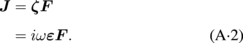
The dielectric tensor ε is obtained from the relation between the density current and electric field F. Here, A, ζ, and ω are the vector potential, electric conductivity, and angular frequency, respectively. Using the interaction picture of the wavefunction and interaction Hamiltonian, Eq. (A·1) is transformed to
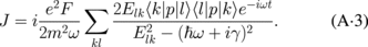
The component of the electronic transition in the dielectric function, εVC(ECV), is expressed using reduced density of states (DOS) ρr and the quasi-Fermi functions for electrons Fc(E) and holes Fv(E), which include the chemical potentials:38)


The effective transition matrix element is expressed by |Pa|2, which is the sum of the contributions from the  ,
,  , and
, and  hole bands. Since the hole-splitting energies are approximately 20 meV, the transition processes related to the three hole bands are included in the observation energy range of the absorption coefficient spectrum. The band-edge energy structure is schematically depicted in Fig. A·1. The broadening factor of the transition is denoted by γa. Assuming the parabolic VB energy structure with the effective mass mh, ρr is calculated. The reduced mass mr is expressed as
  . The energy dispersion curve of the conduction band Ec in the vicinity of ke = 0 is expressed as a function of the electron wavevector ke on the basis of k · p perturbation theory using the wavefunctions of the conduction band and three hole bands:38)
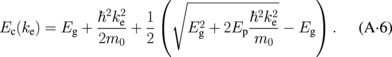
Ep related to the transition matrix element P is defined by  . The critical points with higher energy have minimal effect on the electronic energy structure near the Γ point below 1 eV. For the effective electron mass, the formula
  is used:

At the Γ point of ke = 0,  .
.

Fig. A·1. Schematic drawing of the energy structure around the band edge.
Download figure:
Standard image High-resolution imageThe effective hole mass at the  point of 0.59 (±0.05) m0 was obtained in Sect. 2. The mass values of the spin–orbit split hole (at the
  point) and the crystal field-split hole (
 point) were taken from the analogy of the case of GaN with the same hexagonal crystal structure and almost the same hole splitting energies;93,94) in the kx and ky (j = ⊥) components the light hole mass at the
  point (mlh) is 10% of the heavy hole mass mhh at the
  point, and the crystal field splitting hole mass at the
  point (mch) is the same as mhh, and in the kz (j = ∥) component the light hole mass is the same as mhh for the
  point and 10% of mhh for the
  point.
In the calculation of the Fermi level, a representative hole mass reflecting the total DOS of the three hole bands was calculated. In this case mh satisfies the relation
The direction of the k vector is denoted by x, y, z. In the case of  ,
,  is 0.74. In optical absorption and emission, the dependence of the selection rule on the optical polarization was taken into account. In the above simplified model, the total DOS weighted by the ratio of the oscillator strength for each transition91) was found to be proportional to 1.13
  . This value is discussed in Sect. 2 in conjunction with |Pa|2 in Eq. (A·4). The selection rule in the electron–hole recombination is derived from the symmetry operation and irreducible representation of the C6v4 space group. An insight from the selection rule of angular momentum is possible. When the quantization axis is fixed as the c-axis, the projections of the total angular momentum mJ, orbital angular momentum mL, and spin ms = ±1/2 are defined. The selection rules in the changes of the projections are ΔmJ = 0, ±1, or
  = (0 or ±1, 0 or ±1). When the spin–orbit coupling is rigid, the good quantum number is J.
The PL spectrum IPL(E) was formulated as a function of photon energy E by taking account of the instrumental broadening factor γm and another broadening factor γcv due to the relaxation of the k-selection rule and the inhomogeneity of crystals such as the potential fluctuation around defects:

Here  is the Gaussian function with variable η and broadening factor γ. The refractive index is denoted as n and depends on the transition energy. The chemical potential of holes was taken so that the hole density matched the experimental conditions.
Appendix B: Dielectric function in phonon and plasmon energy region
The component of the phonon and the plasmon terms εppj(E) in the dielectric function for the vibration direction j is expressed as follows. In the reflectance analysis this type of function based on the LO phonon–plasmon coupled (LOPC) vibration modes was utilized:
Here, the subscripts + and − indicate the LOPC+ and LOPC− modes, respectively. The subscript j means the atomic or electronic vibration direction parallel (j = ∥) or perpendicular (j = ⊥) to the c-axis. When γij is small, for instance less than 150 cm−1, E±j is approximated as follows. Here i indicates the vibration mode (T: TO, L: LO, p: plasmon, +, and −):
When γpj becomes large (200 cm−1 or larger), the discrepancy between the LOPC mode energies and the energies obtained from Eq. (B·2) is not negligible. In Refs. 45, 47, and 95, the LOPC mode energies were obtained from the equation ε(E) = 0. The obtained dispersion curve is shown in Fig. A·2. This dispersion curve was required for the analysis of hole properties in p-InN.

Fig. A·2. Dependence of LOPC mode energy dispersion on plasmon broadening. The vibration direction is perpendicular to the c-axis.
Download figure:
Standard image High-resolution image
The parameters for GaN layers were obtained in advance using the dielectric constants at the infinite frequency of ε∥(∞) = 5.01ε0 and ε⊥(∞) = 5.04ε0.96,97) For InN the isotropic reflectance oscillation period was found to be in the region of 1200–4500 cm−1; thus, we adopted the isotropic value of 7.0ε0 for films with a low electron density on the order of 1017 cm−3, and εj(∞) increases with increasing in residual electron density.27) The scattering rates of the modes are denoted by γij. The plasmon energy Epj is expressed as ħ(nke2/εj(∞)mkj)1/2, where mkj is the effective mass of electrons (k = e) or holes (k = h) and nk is the carrier density. The broadening factor γpj was taken as the lifetime broadening. The optical electron or hole mobility  is defined as ħe/mkjγpj. Although the next formula Eq. (B·3) is a function directly expressing the phonon and plasmon components, Eq. (B·1) is appropriate for reproducing the experimental spectra:
Here, sij and εj(0) are the oscillation strength of the TO mode with energy ETj and the static dielectric function with vibration direction j, respectively. Equation (B·1) includes four broadening factors of γ+j, γ−j, γpj, and γTj, although Eq. (B·3) includes only two broadenings factors, γpj and γTj. In most semiconductors, there is a discrepancy between the experimental and theoretical spectrum shapes when using Eq. (B·3) in the region from the Reststrahlen band to the edge of the LOPC+ mode energy. This is thought to be because the constant broadening factors of the TO phonon and the plasmon are inadequate for the expression in the wide energy range of the LOPC− and LOPC+ modes. In the case of  cm−3 for the example of InN, the energy difference between these two energies is as much as 400 cm−1. Equation (B·1) is an approximated formula expressing the dependence of γpj, and γTj on energy by adopting the four representative broadening factors.
Appendix C: Rate equation analysis
The PL intensity and its dependence on temperature were analyzed using the following rate equations of the electron and hole densities:


Here, the densities of holes in the valence band, localized holes, electrons, all deep states, and occupied deep states are denoted as nh1, nh2, ne, nt0, and nt, respectively. The radiative recombination rate coefficients of the holes in the valence band and the localized states are B01 and B02, respectively. F12 and F21 are the rates of the hole transition from the valence band to the localized states and that of the inverse flow. Bth and Bet are the rate coefficient of the electronic transition from the deep states to the valence band and that from the conduction band to the deep states, respectively. L1 and L2 are the hole generation rates. In the case of n-type materials, all deep states were assumed to be occupied by electrons, thus

From the rate equations the density of the free holes was obtained. L2 was expressed as βL1, where β is a constant between 0 and 1:

Here A10 = B10ne0, A20 = B20ne0, and A11 = Bthnt0 were used. The PL intensity was expressed as

The next formula was obtained by adopting the relations F21/A02 = a1 exp(−Es/kbT), A11/A01 = a2 exp(−Enr/kbT), and a3 = F12/A01, where a1, a2, and a3 are constants. Es and Enr are the hole localization energy at shallow levels and the activation energy of NRR, respectively. The transition rate of holes from the valence band to the localization states was assumed to be much larger than the radiative recombination rate of localized holes:

When we assume F21/A02 ≫ 1, the following expression is obtained. This assumption is based on the greater number of states or the greater statistical weight of the valence band maximum than that of the localization levels:

Note that the expression ![$I_{\text{PL}}(T) = 1/[1 + \sum_{i}a_{i} \exp ( - E_{i}/k_{\text{b}}T)]$](https://content.cld.iop.org/journals/1347-4065/53/10/100204/revision1/STAP07012if118.gif) is valid only when Es ≪ Enr and a1 exp(−Es/kbT) ≪ 1. The former condition cannot be assumed: furthermore, at a temperature of 15–300 K, the latter assumption is also invalid.
is valid only when Es ≪ Enr and a1 exp(−Es/kbT) ≪ 1. The former condition cannot be assumed: furthermore, at a temperature of 15–300 K, the latter assumption is also invalid.
In the case of p-type samples, the spectra were analyzed using the PL intensity of the band-edge emission IPL1 and that of holes trapped at the shallow levels IPL2. In the p-type samples the NRR rate under a weak excitation condition was approximated as being proportional to the product of nh1 and ne: the occupation probability of deep states was proportional to the electron density. Thus Bthnh1nt0 is replaced by B1nh1ne. The ratio B1/B01 was obtained from the sum of Eqs. (C·2a) and (C·2b): B1/B01 = (L − IPL2)/IPL1 − 1, where L is the sum of L1 and L2. B1/B01 is expressed as (T)β exp(−Enr/kbT). When the mean free path of carriers determined by the product of the carrier velocity vc and the carrier scattering time 1/γc (approximated by the plasmon scattering time 1/γpj) is greater than the mean distance between the NRR centers, β is 1/2; otherwise β can be smaller or greater. For the n-type InN films investigated in Refs. 45, 87, and 88, the increase in γp⊥ with the increase in temperature from 5 to 100 K was found to be within 20% of the value at 5 K, and thus β was estimated to lie between 0 and 1/2:

Here, C and L are fitting parameters.
Biographies

Yoshihiro Ishitani was born in Shizuoka, Japan, in 1965. He received B.E., M.E., and Ph. D. in engineering science from Kyoto University, Kyoto, Japan, in 1989, 1991, and 1999, respectively. After he worked at Hitachi Central Research Laboratory as a researcher and at Hiroshima University as a research associate, he became an associate professor at Chiba University. He is currently a professor at Graduate School of Electrical and Electronic Engineering, Chiba University. His research interest includes physical properties of semiconductors particularly for III–nitrides and dynamics of carriers and phonons in optical device materials. He is a member of Japan Society of Applied Physics (JSAP), The Physical Society of Japan (JPS), and Japanese Association for Crystal Growth (JACG).