
Abstract
We present the first tunable v-shaped mirror, also known as Fresnel mirror, that may be used to generate a quasi-nondiffracting line pattern, for example for applications in laser lithography or nanomachining with femtosecond lasers. The aperture of the device is 5 mm with a surface flatness of better than λ/10, and the range of the tilting angle is 1.3–38 mrad, resulting in a fringe spacing of 123 μm down to 4.2 μm for red light at 633 nm. In contrast to usual cantilever-comb setups, the mirrors are supported on a PDMS layer and tilted by a single piezoelectric actuator, providing a high resonance frequency of 5.1 kHz. The device is fabricated using laser rapid prototyping of silicon and a casting processes of soft polymers. We show the static and dynamic characterization of the mirror and the verification of the optical functionality.
Export citation and abstract BibTeX RIS
1. Introduction
In this paper, we present the first Fresnel mirror with adjustable tilting angle. The original Fresnel mirror, not to be confused with a Fresnel lens, was an apparatus with two mirrors that were inclined at a small angle relative to each other, which allowed the observation of interference patterns in the reflected light from an incoherent source [1] and helped to prove the wave nature of light [2]. The availability of coherent laser sources brought new applications for this old principle. The two mirrors are typically used to split the light of a collimated laser beam into two coherent overlapping light sheets with planar wavefronts. Within this zone, an interference pattern is formed, that propagates along the optical axis without broadening. Compared to a projected stripe pattern generated, e.g., by an image projector or an array of cylindrical lenses, the Fresnel mirror pattern can be regarded as quasi-nondiffracting, or propagation invariant and self-healing, similar to the central maximum of a Bessel-beam generated by an axicon (for the properties of Bessel-beams see e.g. [3–6]). If the pattern is obstructed in one point by an object like dust on a window or debris generated by laser machining, the interference fringes will form again further down the optical axis, and as a first order approximation, the size of the patterns depends mainly on the wavelength of the light and the tilting angle of the mirrors.
This interference pattern has initially been used to structure linear optical gratings into photoresist [7] without the need for a high-resolution photomask. Another application are structured light 3D-scanners, where the stripe pattern is projected onto an object and the distortion of the lines is recorded at an angle by a camera to measure the surface topology. The so far only integrated microelectromechanical systems (MEMS) Fresnel mirror was produced by Oka et al [8] for a microfluidic diffusion sensor. In that design, the static mirrors are first fabricated in the plane and deflected by stiction after a sacrificial wet etching process. The resulting interference pattern with green laser light generates laser-induced dielectrophoresis, which is used to determine the diffusion coefficient of proteins.
Recently, we proposed the use of an adaptive Fresnel mirror for direct nanomachining of sub-wavelength structures into silicon or dielectric substrates by laser-induced periodic surface structures (LIPSS), generated by femtosecond laser pulses [9–11]. In this application, the Fresnel mirror is intended to deliver a sharp line pattern, while introducing only a minimal amount of optical dispersion into the system. LIPSS are formed by the interference of the incident light pulse with scattered light or a surface plasmon that is generated in the material [12]. If the light is structured into a line focus, nanostructures can be achieved, that are coherently linked over an extended area. These nanoripples are interesting for a number of applications, for example as functional materials for photovoltaics, superwetting and gas sensors [12]. For a review on LIPSS see [13].
Such applications require fast switching speeds and a certain robustness to handle high pulse energies. This is realized by our new design principle, in which we micro-structure and elastically bond a rigid mirror surface onto a PZT piezo bending actuator using economic, cleanroom-free prototyping processes, producing a compact composite device.
The paper is organized as follows: in section 2, we describe the design layout and show the mechanical simulation of the device and an estimation of the intensity distribution of the reflected beam. After the fabrication process in section 3, we discuss the mechanical and optical characterization in sections 4 and 5 and summarize our results in section 6.
2. Design and working principle
The design of the tunable Fresnel mirror consists of two movable mirror segments that are joined in the center line of the device. In the initial position, the mirrors feature a downward deflection. Upon actuation, the deflection of the mirrors is adjusted, which alters the mirror angle. The two mirrors are fixed on a soft silicone (PDMS) layer and are not held by cantilever springs, as opposed to conventional MEMS mirrors (e.g. [14]). Cantilever springs are easily damaged by high power laser pulses since the heat transfer through thin silicon structures is slow [15]. The cantilever avoiding design features the additional advantage, that larger deflections can be realized with a narrow hinge region.
The two mirrors are actuated by a piezoelectric bimorph bending disk, that is attached underneath the PDMS layer. Upon actuation, the piezo disk performs a spherical deflection, which results in a pressure load on the soft PDMS. As a result, the two mirrors are pulled downwards as illustrated in figure 1. The main design parameters for a maximal change in mirror angle are the choice of the piezoelectric material, the geometry of the hinge, the thickness of the PDMS and the Young's moduli of the base PDMS and the PDMS in the hinge region. The geometry of the hinge is designed to be trapezoidal. On the mirror side, the hinge is chosen to be as narrow as possible by the chosen fabrication process. At the bottom, the hinge has to be wider to allow for a tilting movement. The influence of the choice of PDMS is investigated by finite element method (FEM) simulations.

Figure 1. Schematic working principle of the tunable Fresnel mirror: The deflection of the bending actuator induces stress in the soft PDMS layer, which pulls down the mirrors.
Download figure:
Standard image High-resolution image2.1. Mechanical modeling by FEM-simulations
The device is modeled in 3D with quarter symmetry in SolidWorks and simulated in COMSOL Multiphysics via the LiveLink interface. The mirrors feature a thickness of 300 μm and a size of 2.5 × 5 mm2 each. The total chip outline is 10 × 10 mm2 and the diameter of the circular piezo bimorph is 14.2 mm, hence, it covers the full chip area. The thickness of the actuator is modeled as 240 μm. A simple linear model is employed for the simulations, which is sufficient for the small strain levels of <10% that we expect [16]. Figure 2 shows the model with mesh and the boundary conditions. The chip is fixed at a rim on the top outer edge, the rest of the structure is free to move.
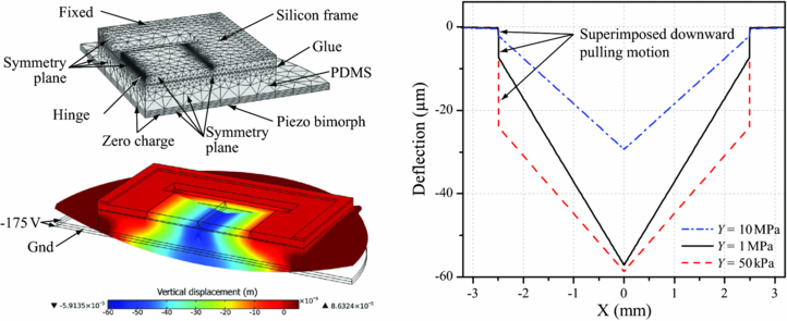
Figure 2. Simulation result of the deflection of the mirrors for three different Young's moduli of the PDMS hinges. For very soft hinges, the deflection is increased but the mirror angle is getting smaller. Stiff hinges lead to low deflection and a low mirror angle.
Download figure:
Standard image High-resolution imageThe Young's modulus and Poisson ratio of silicon are taken from the COMSOL material library. The glue that connects the chip with the base PDMS (SilPoxy by Smooth On) is rated with a Shore A hardness of 40, which can be converted to a Young's modulus of 2.0 MPa [17]. All silicones are considered to be nearly incompressible with a Poisson ratio of 0.49. We use a PZT-ceramic, where 15% of lead is substituted with strontium, for which no compliance matrix is available in the literature. The piezoelectric bending actuator is therefore modeled with the compliance matrix for PZT-5H multiplied with a correction factor of 1.16, that was determined by a preliminary frequency measurement with a shaker to match the resonance frequency of a cantilever beam predicted by the simulation with the experiment. The voltage is multiplied with a correction factor of 1.21, that was estimated by measuring the deflection profile of a bimorph actuator mounted on a PDMS supporting ring, and comparing it to the profile predicted by the simulation, to account for the larger d31 and d33 coefficients of the material compared to PZT-5H [18].
The thickness and stiffness of the base PDMS play one major role in the performance of the device. By applying a sweep, a thickness of around 1000 μm at a Young's modulus in the range of 200 to 400 kPa was found to be a good compromise between optimal performance and ease of fabrication. With this configuration, the maximum mirror angle changes by less than 1.5% in that stiffness range. For thinner PDMS layers in the range of 500 μm, the Young's modulus of the PDMS would have to be reduced drastically, which would result in a gel-like material.
With respect to the PDMS hinges, there are two possible scenarios during actuation that are illustrated in figure 2: if the stiffness of the hinges is too large (blue line), the rotation of the compliant hinge is suppressed; if the stiffness is too low (dashed red line), the rotation is superimposed with a downward pulling motion that leads to a reduced mirror angle. The optimum stiffness range is calculated by a sweep with an increment of 50 kPa. Within a range of Y = 0.45 to 1.35 MPa, the mirror angle is within 98% of the maximum value. This suggests that the tolerance of the PDMS-stiffness has only a minor effect on the maximum mirror angle that can be achieved by the actuation. The deflection for a Young's modulus of 1 MPa is illustrated by the solid black line in the figure.
With this configuration, the piezoelectric bimorph can tune the deflection in a range of ±56 μm, which translates to a mirror angle of ±19.8 mrad. Since positive deflections lead to a diverging beam that cannot be used directly in most applications, a downward predeflection of 55 μm is set during fabrication, so that the maximum angle is expected to be in the range of 40 mrad.
The optimized model is also used to estimate the influence of the thermal expansion of the polymer parts on the mirror angle. PDMS exhibits a large coefficient of thermal expansion of 2.6 × 10⁻⁴ 1/K [19], but the dominant motion of the isotropic expansion is a downwards movement of the unclamped actuator and not a change in tilting angle. For a temperature change of 1 K, the actuator moves down by 0.7 μm, which is a factor of 7 larger than the motion of the mirror. The change in the mirror angle is −37 μrad K−1 and can therefore be neglected if the device is operated under laboratory conditions.
2.2. Analytic estimation of the optical function
The optical configuration of the tunable Fresnel mirror to produce a line pattern is illustrated in figure 3. The Fresnel mirror reflects the incoming plane wave laser beam in two tilted outgoing plane waves into an overlapping zone, where the interference pattern is formed. In this section, we perform a geometric estimate for the parameters describing the fringe spacing of this line pattern.

Figure 3. Working principle of a Fresnel mirror. The incident laser beam is split into two converging light sheets that overlap and form interference fringes. The spacing of the fringes and the length of the overlapping zone is adjusted by the tilting angle of the mirrors. In practice, we use an orthogonal incident beam via a beam splitter as shown in figure 14. The diverging far field can be focused by additional lenses to again form interference fringes further down the optical axis.
Download figure:
Standard image High-resolution imageConsidering a mirror with tilting angle β and width w for each mirror segment, the geometric length of the interference zone is

and at its widest point, the width is approximately equal to w/cos (2β) ≈ w. Here and in the following, the relative accuracy of the small-angle approximation is β2, so the approximation is sufficient for practical purposes.
To obtain a geometric result for the line spacing Δx, we assume an incoming plane wave in the negative z direction. We then calculate the path difference Δl of light being reflected by the two mirror segments into the same point at some position xi and apply the requirement  for constructive interference. In the center at x = 0, the path difference vanishes, so there will be an intensity maximum.
In figure 4, we illustrate this phase shift using a ray that intersects the orthogonal plane at the apex of the Fresnel mirror at a height of x = h. This parameter h describes all light rays that are reflected by the mirror. As the problem is invariant over an overall path shift, and we want to have a description independent of the position of the image, we can take l = −(l1 + l2) to parametrize the optical path, with l = 0 for a ray incident at h = 0. Looking at the triangle of l1 and l2 + l3, we find that l1 = l2 + l3, and from the triangle of h and l2 + l3, we see l1 = l2 + l3 = htan β. Further, the triangle of l1, l2 and h' tells us that h' = l1sin 2β = l2tan 2β, such that l2 = l1cos 2β = l1(1 − 2sin 2β). Fusing the parts, we arrive with l = −2htan β (1 − sin 2β). If we look at an image point xi, zi in the inset of figure 4, this is illuminated both from the upper and lower mirrors with rays described by hup and hlow with path lengths lup and llow. For points on the axis, xi = 0, we have trivially hup = hlow = h0 and hence lup = llow = l0, so there is constructive interference. As we shift this to some off-axis point, symmetry tells us that hup = h0 + xi and hlow = h0 − xi with a corresponding optical path lup = l0 − 2xitan β (1 − sin 2β) and llow = l0 + 2xitan β (1 − sin 2β). Hence, constructive interference is achieved whenever Δl = lup − llow = −4xitan β (1 − sin 2β) = nλ, such that the maxima are separated by

The approximation for small angles can be straightforwardly understood, as the phase shift in the light sheet of the two mirror segments is approximately ±2βx. The total number of lines is nmax = wcos (2β)/Δx ≈ 4βw/λ. If the illuminating beam is narrower than the pair of mirrors, w has to be adjusted in these expressions accordingly.

Figure 4. Sketch of the geometric consideration that yields the fringe spacing of the interference pattern. β denotes the mirror angle, (zi, xi) is the position of the image plane. The inset shows the full ray path for the central and first off-axis maximum, the big figure highlights the details of a generic ray used in the calculation.
Download figure:
Standard image High-resolution imageFor the maximum expected mirror angle of 40 mrad and the case of full illumination, the length of the zone is 31 mm. This means that the center of the overlapping zone is 15.5 mm in front of the mirror, which could cause problems because of interference with the incident beam or shadowing effects. In combination with a red laser at 632.8 nm, a maximum of 630 fringes with a spacing of 4 μm are generated. For a UV-laser at 355 nm, the spacing of the fringes would be reduced to 2.2 μm. Thus, the achievable mirror angle is sufficient for the direct writing of optical gratings, which requires the smallest fringe spacing of the applications mentioned above. Larger spacings can be adjusted by reducing the mirror angle or by an additional external telescope optic.
3. Fabrication of the adaptive Fresnel mirror
The fabrication of the adaptive Fresnel mirror relies solely on rapid prototyping processes and does not require a cleanroom. The process starts with a 300 μm thick silicon substrate, that is coated with a 300 nm thick aluminum layer. This reflective optical surface is protected by a layer of AZ9260 photoresist during the subsequent processing, which is indicated in figure 5(a). In the first step, the mirror hinges are cut through the silicon by direct laser ablation with a UV-marking laser (Trumpf TRUMARK 6330) at a wavelength of 355 nm and a mean output power of 2 W. The diameter of the focused laser spot is 25 μm. A more detailed description of our setup is explained in the publication by Meier et al [20]. Laser debris is removed in an ultrasonic bath in deionized (DI)-water. To prevent the photoresist from delamination during this process, the mirror layer is additionally protected by a slab of PDMS. The trenches are cut sequentially, starting with a large linewidth that decreases with increasing depth to achieve a trapezoidal shape. On the backside, the trenches feature a width of 140 μm whereas on the mirror side, the width of the trenches is smaller than 10 μm, as shown in figure 6.
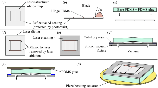
Figure 5. Fabrication process of the adaptive Fresnel mirror. The processing steps of the mirror chip (a)–(d) are performed on a wafer level. The laser cleaning step (e) removes residual dust from dicing. The individual chips are then placed into a vacuum mount, where the predeflection is set (f) and the actuator is glued on the PDMS layer (g).
Download figure:
Standard image High-resolution image
Figure 6. Micrograph of the laser-structured mirror trenches: view from the backside (a) and from the mirror side (b). Photograph of the assembled device in the chip mount (c) and micrograph of the electrical solder connection on piezo-actuator (d).
Download figure:
Standard image High-resolution imageThe silicon backside and the mirror hinges are treated with an adhesion promoter (Dow Corning 92-023) and liquid PDMS is poured over the wafer to fill the gaps in the hinges. A vacuum of 10 mbar removes trapped air bubbles. The Young's modulus of the PDMS is adjusted to 1.197 ± 0.055 MPa [16] by mixing RTV615 (Momentive Performance Materials) with 10% silicone thinner (200 fluid 50 cst by Dow Corning). Excess PDMS is scraped off the wafer with a blade as indicated in figure 5(b), and the PDMS is cured in a convection oven at 120 °C. The 1 mm thick layer of soft base PDMS with a Young's modulus of 0.2 MPa [21] (RTV23 by Neukasil) is fabricated separately in a hot pressing machine and glued on the backside of the wafer using silicone glue (SilPoxy by SmoothOn), as illustrated in figure 5(c). In the next step, the wafer is aligned in the UV-laser with the mirror side facing up. On each chip, a rectangular opening is cut through the silicon at the outline of the mirror segments as illustrated in figure 5(d). The mirrors are now only held by PDMS and are free to move. The wafer is once more aligned under the laser, this time with the mirror side facing down, and the chips are diced. A glass handle substrate helps to prevent scratches in the reflective layer. A laser hatch is used to remove residual dust and laser debris from the edges of the element as shown in figure 5(e). The individual chips are placed into a chip mount and cleaned with DI-water in an ultrasonic bath.
The chips are dried in a convection oven at 60 °C. Afterwards, they are aligned on a vacuum mount with a 55 μm thick bar of photoresist in the center, which adjusts the predeflection of the mirror segments (figure 5(e). This structure is fabricated on a silicon wafer by laser ablation, as are vacuum interconnects of the mount. A 120 μm thin layer of silicone glue is applied on the pre-fabricated piezo-actuators by squeegee technique with a Kapton stencil mask. The actuators are then glued on top of the chips (figure 5(f)). Even though alignment is not critical for this last step, an alignment tool is used to place the actuator in the center. The glue cures at room temperature for 15 min. The finalized chips are then glued into the laser-structured FR2 PCB-substrate in figure 6(c) for better handling. The residual layer of photoresist is then removed with acetone in an ultrasonic bath.
The piezo-actuator consists of two 120 μm thick sheets of commercially available strontium-doped PZT ceramic (by Ekulit) with 5 μm thin silver electrodes. The first sheet is cut to a circular shape with a notch, that allows contacting the intermediate electrode, and two thin alignment crosses are marked into the top electrode. The part is then glued with anti-parallel direction of the polarization on top of the second ceramic sheet using epoxy glue and left to cure on a hotplate. After an alignment, the circular outline of the actuator is cut with the laser. Since the maximum voltage during operation is close to the breakdown-voltage of air, a 200 μm wide rim of the electrode layer is removed from the edge of the actuator by a laser hatch. The top, bottom and one middle layer are connected with thin insulated leads by soldering (figure 6(d)).
4. Mechanical characterization
The assembled device is placed into a custom designed mount that on the one hand, allows the integration into an optical setup and on the other hand also contains an electrical protection circuit that prevents the piezo sheets from depolarization. Figure 6(c) shows the mount and the circuit, the schematic of the circuit is depicted in the inset of figure 10. The circuit design is adapted from Ruschmeyer et al [22], the Zener diodes regulate the electric potential of the middle layer of the piezo so that the maximum electrical field in counter direction of the polarization does not exceed 1/3 of the coercive field strength. In combination with the two resistors, the Fresnel mirror is controlled with one ac or dc input signal. A photograph of the assembled device on an optical bench is shown in figure 7. A square aperture minimizes unwanted reflections.

Figure 7. Photograph of the final device mounted on an optical bench. An additional square aperture is used to minimize unwanted reflections.
Download figure:
Standard image High-resolution imageThe deflection of the mirrors for the maximum DC voltages of ±350 V is measured with a scanning white-light interferometer. The result in figure 8(a) and (b) shows a maximum mirror angle of 38.1 mrad for a DC voltage of 350 V, which is is close to the expected angle of 39.6 mrad. The minimum angle at −350 V in figure 8(c) is 1.28 mrad, hence the maximum change of the mirror angle is 36.8 mrad, which is 7.6% smaller than expected by the simulation. The minimum angle agrees closely with the design goal and is in the range of the assembly accuracy, which leads to an off-axis tilt of the two mirror segments of θ = 0.72 ± 0.04 mrad at −350 V and θ = 0.68 ± 0.15 mrad at 350 V respectively. This tilting angle is clearly visible in figure 8(c) and relates to a deflection of 3.6 μm across the mirror length of 5 mm. It originates from a combination of bow of the alignment tool in figure 5(f) and residual dust or molten material from the laser process. The flatness of each mirror segment is evaluated along three cuts in horizontal and vertical direction. The data shows a slight parabolic bending profile with an Ra value of 21.9 nm for the defocused state at −350 V, and 112 nm at 350 V. This translates to a focal point of 29.1 m for −350 V and 4.3 m for 350 V. The bending effect of the actuator is thus detectable in the mirror deflection, however only to a small extent, that will not impede the optical function of the device. The maximum working distance is a factor of 30 to 133 smaller than the focal point of the mirrors.
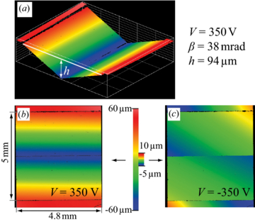
Figure 8. Whitelight interferometric measurement of the deflection of the mirror for different for different DC voltages: 3D representation of the deflection at 350 V (a) and top views at 350 V (b) and −350 V (c).
Download figure:
Standard image High-resolution imageThe dynamic deflection of the mirrors is measured with a triangulation sensor (Keyence LK-G10) in combination with a computer controlled X-Y-stage (2 × Micos LS110). The triangulation sensor measures the absolute position at one point, and the stage is used to move the sensor over the sample. A sinusoidal signal is applied to the Fresnel mirror, and the measurement of the triangulation sensor is triggered to be in phase with the driving signal. The displacement is measured at one point as a function of time. This measurement is repeated for multiple points on the mirror to obtain a two-dimensional image of the deflection for one period. To increase the resolution of the measurement, 20 periods are captured for each point, and the average value is calculated for each time step. Static measurements are performed by moving the sensor continuously at a speed of 0.5 mm s−1.
Figure 9 shows a line scan for a low frequency of 0.5 Hz and a driving signal with an amplitude of 350 V. The maximum change in mirror angle of 28.7 mrad is 22% lower than for the scan with the white-light interferometer and 27.5% lower than in the simulation, which is due to the creeping effect of the piezoceramic actuator. The measurement also confirms the function of the mirror hinges during actuation. Without an applied voltage, the hinges are not deflected. For positive voltages, the hinges are pulled downwards, but the dominant motion is still the tilting of the mirrors. For negative voltages they are pushed upwards, however to a smaller extent. Over the full voltage range the hinges are deflected by 11.4 μm, which is close to the value of 10.6 μm predicted by the simulation.
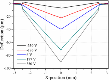
Figure 9. Measured deflection profile across the center of the mirror for a sinusoidal driving signal with f = 0.5 Hz and an amplitude of 350 V for different points on the hysteresis loop.
Download figure:
Standard image High-resolution imageThe hysteresis and the frequency response of the change in mirror angle are determined by measuring the deflection at two points for each mirror segment over one period. The measurement principle is also illustrated in the inset of figure 11. For the hysteresis measurement, a low frequency of 0.5 Hz and different amplitudes ranging from 100 to 700 Vpp are used. The frequency response is recorded for a range of frequencies at a fixed amplitude of 10 Vpp. Larger amplitudes would lead to the destruction of the actuator at resonance.
The measurement in figure 10 shows the typical hysteresis behavior of piezoceramic actuators. For signal amplitudes larger than approximately 300 V, the actuator starts to reach saturation. The width of the hysteresis loop prevents a direct voltage control of the mirror angle, however many approaches like closed-loop control [23] or open-loop [24, 25] hysteresis compensation exist and can in principle also be employed with this actuator. Another approach that is especially applicable for short pulse lasers is to apply a continuous sinusoidal driving signal to the actuator and trigger the laser shutter to a certain phase difference. Since the change in mirror angle during one laser pulse is negligible, the mirror angle is then defined solely by the phase difference. For this concept, the phase of the mirror angle with respect to the driving signal has to be characterized. Figure 11 shows both the frequency response and the phase shift of the mirror angle. Both values are taken from a sine-fit for each frequency. At 5.1 kHz a sharp resonance peak is visible, along with a characteristic drop in the phase shift to −π and a further decrease for higher frequencies. The peak shows a width of 700 Hz and a side-peak in the range of 2.1 to 2.9 kHz, which suggests that the system is nonlinear and therefore more susceptible towards the excitation of higher order resonances. In that range a positive phase shift occurs. Until a frequency of approximately 1.5 kHz however, both the phase shift and the change in amplitude are negligible.

Figure 10. Hysteresis curves for sinusoidal driving signals with a frequency of 0.5 Hz and different amplitudes. The inset shows the protection circuit that prevents depolarization of the piezo.
Download figure:
Standard image High-resolution image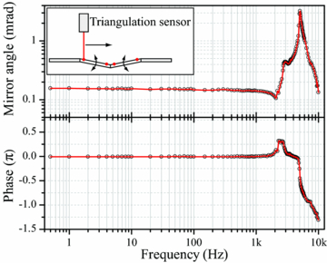
Figure 11. Frequency response of the mirror angle for a sinusoidal driving signal with an amplitude of 10 Vpp.
Download figure:
Standard image High-resolution imageThe excitation of higher order resonances becomes obvious by plotting the normalized progression of the mirror angle for one period and multiple frequencies. Figure 12 proves that for frequencies lower than resonance, the mirror angle follows a sinusoidal shape. Within the first peak at 2.4 kHz, a significant deviation from a higher order resonance is visible. The effect is even more pronounced at the main resonance peak, where a frequency of 44.6 kHz appears to be superimposed on the signal. Since this frequency is close to the sampling frequency of 50 kHz of the laser-triangulation sensor, this aspect can not be investigated further with our setup.

Figure 12. Progression of the mirror angle during one period for different frequencies at a signal amplitude of 10 Vpp. The amplitude of the change in mirror angle is normalized to 1. The inset shows a magnified view of a section of the signal.
Download figure:
Standard image High-resolution image5. Optical characterization
The optical functionality of the Fresnel mirror is characterized with a He–Ne laser at a wavelength of 632.8 nm and a CMOS camera with a pixel pitch of 2.2 μm mounted on a linear stage. The light is collimated by a 40 mm aspheric lens and expanded to a diameter of 17.8 mm. The beam is apodized to achieve a near flat-top intensity profile, a sketch of the setup is shown in figure 13. With this setup the Fresnel mirror can only be characterized in the static operation mode since the CMOS camera features a rolling but not a global shutter. Dynamic measurements would lead to a distorted image, even if a trigger and a short exposure time are applied.

Figure 13. Measurement setup for the static optical characterization of the interference fringes. The lenses L1–L3 collimate the light and the neutral density filter reduces the intensity of the beam. The camera chip is placed in the center of the overlapping zone.
Download figure:
Standard image High-resolution imageFirst, a DC signal is applied to the mirror and after a waiting time of several minutes to account for creeping, the tilting angle of the mirrors is measured with the laser-profilometer. The device is then placed in the optical setup, and the interference pattern is recorded in the center of the overlapping zone. Creeping effects of the piezoceramic still occur during this time, but the magnitude of the change in mirror angle during the experiment is less than 4% and therefore negligible. The camera is rotated until the fringes are aligned parallel to the pixels to minimize the moiré effect.
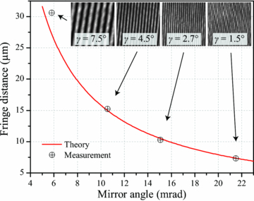
The period of the interference fringes is evaluated by a spatial FFT analysis of the intensity pattern. Figure 14 shows the result for four mirror angles from 5.8 mrad to 21.5 mrad in comparison to the values predicted by equation (2). Larger mirror angles lead to an interference pattern with tightly spaced fringes that can not be resolved with the current measurement setup. The insets show a 220 × 220 μm2 large section of the intensity distribution. The theoretical prediction of the fringe spacing corresponds well to the measured values with a deviation of less than ±2%, with the exception of the smallest measured angle of 5.8 mrad. Here, a deviation of 12.2% is visible. This is most likely due to a combination of both the creeping effect of the piezoceramic and the in-plane tilting angle θ, that is also visible in figure 8(c). This tilting effect is also responsible for the rotation γ of the fringes with respect to the geometrical edge of the mirror. The individual values for γ are noted in the insets of figure 14 and range from 7.5° for 5.8 mrad to 1.5° for 21.5 mrad.
Figure 14. Measurement results of the fringe spacing for different mirror angles in comparison with the theoretical values of equation (2). The insets show a section of the recorded interference pattern. The tilting angle γ between the fringes and the geometrical edge of the mirror is noted in the insets.
Download figure:
Standard image High-resolution image
6. Summary and conclusion
In this paper, we presented and validated the concept for the first tunable MEMS Fresnel mirror. In contrast to classical cantilever-spring-type MEMS designs, the mirror segments are bonded via a soft polymer substrate to a piezo bending actuator as we described in section 2. This allows for an economic prototyping process described in section 3, without the need for a cleanroom, and provides a robust device that can in principle support high pulse energies. Based on this concept, the device was designed and optimized using a finite element simulation of the mechanical behavior described in section 2.1 and verified with a functional prototype.
The mechanical characterization of section 4 showed a tuning range of the mirror angle of 36.8 mrad and gives together with the adjustable offset angle of 19.7 mrad in our prototype a working range of 1.28–38.1 mrad. The resulting line width of 124 μm down to 4.16 μm and interference zone length ranging from 977 to 32.8 mm makes it suitable for a wide range of applications. Using white-light interferometry, the device was found work accurately up to an off-axis tilt of the mirrors of θ = 0.7 mrad relative to each other, which is due to tolerances and residual particles on the alignment tool. The flatness of the mirrors is affected to a small extent by the bending of the piezo-actuator and thus a parabolic profile results. The interference zone length, however, is a factor of 30 to 133 smaller than the resulting focal point of the mirrors in the focused and defocused state, respectively. The frequency response obtained from a high-speed stroboscopic measurement using a scanning triangulation sensor showed a cascade of resonances starting at f > 1.5 kHz. Hence, the device is capable of high-speed beam shaping even if it is operated below resonance. We performed a first estimate of the long-term stability by monitoring the amplitude of the deflection over 107 cycles close to saturation. We found that the variation in the deflection stays in the range of noise and other fluctuations for the first 105 cycles and afterwards appears to decrease logarithmically with a few per cent per decade. This behavior and the causes certainly needs to be investigated further, but it suggests that the long-term stability is not a major problem and can be solved e.g. with a burn-in procedure.
To explore the optical functionality, we performed a geometric estimate for the line width and length of the interference zone. We verified the line width in the optical characterization of section 5 by measuring the intensity distribution with a camera and found it to be in very good agreement with the predictions. We also found the artifacts of the parasitic tilting angle θ which leads to a rotation of the fringes with respect to the geometric edge of the device and to an increased fringe spacing at small mirror angles.
We finally conclude that the tunable Fresnel mirror with its new actuation and design concept was successfully verified and the performance goals were achieved. The optical and mechanical quality and the mechanical and electrical packaging of the prototype are already suitable for its use in experiments with laser lithography and LIPSS, which will be the subject of our further investigations. In future developments, the observed rotation of the fringe pattern could be further reduced by optimizing the tolerances of the tooling in the fabrication process.
Acknowledgment
The authors would like to acknowledge the funding of the Deutsche Forschungsgemeinschaft (DFG) under grant WA 1657/3-1 and GR 1782/14-1.