
Abstract
Aligned large-scale deposition of nanowires grown in a bottom-up manner with high yield is a persisting challenge but required to assemble single-nanowire devices effectively. Contact printing is a powerful strategy in this regard but requires so far adequate adjustment of the tribological surface interactions between nanowires and target substrate, e.g. by microtechnological surface patterning, chemical modifications or lift-off strategies. To expand the technological possibilities, we explored two-directional pressure-controlled contact printing as an alternative approach to efficiently transfer nanowires with controlled density and alignment angle onto target substrates through vertical-force control. To better understand this technology and the mechanical behavior of nanowires during the contact printing process, the dynamic bending behavior of nanowires under varying printing conditions is modeled by using the finite element method. We show that the density and angular orientation of transferred nanowires can be controlled using this three-axis printing approach, which thus enables potentially a controlled nanowire device fabrication on a large scale.
Export citation and abstract BibTeX RIS

Original content from this work may be used under the terms of the Creative Commons Attribution 4.0 licence. Any further distribution of this work must maintain attribution to the author(s) and the title of the work, journal citation and DOI.
1. Introduction
The implementation of semiconductor nanowires (NWs) in different fields of nanotechnology, including field-effect transistors [1, 2], light-emitting diodes [3], and a wide variety of sensors [4, 5] has been intensively discussed in the past two decades. The main challenge in NW device fabrication for mass production or at least for a broader range of applications at low cost is the efficient planar assembly of bottom-up grown NWs on various substrate materials. This includes control over their substrate location, angular orientation, and density of transferred NWs [6–8]. Multiple methods for the creation of NW assemblies were reported in this regard comprising, for instance, a bubble-blow technique [3, 9], NW orientation control by fluid flows [10], and Langmuir–Blodgett alignment [11, 12]. Flow-directed and Langmuir–Blodgett techniques allow only limited control over the position and orientation of individual NWs, and they are hardly applicable for small diameter NWs, meaning specifically a diameter of less than 15 nm [7]. The required sample preparation and microtechnological fabrication steps prior to NW transfer appear still too costly and elaborate to be suitable for a broader range of applications. Therefore, they must be considered unsuitable for mass production according to the current state of the art [9].
In contrast, NW contact printing (CP) presented by Javey et al [7, 13, 14] enables transfer and simultaneous parallel alignment of NWs on the target substrate by using mechanical contact and a shearing motion of the NW growth and the target substrate. This process appears intrinsically suitable for a large variety of NW materials [15–17], large-scale assembly of NWs [13] and high-performance electronic devices [7, 18–21]. The electrical properties of the NWs are retained after CP as reported elsewhere [7, 13, 14]. Additionally, the density of printed NWs was enhanced by using octane and mineral oil as lubricants to decrease the mechanical friction between the NWs and the target substrate while applying relatively high printing pressures. Although these techniques are capable of controlling the density as well as the alignment of NWs, in particular lubricants must be critically reviewed in terms of contamination minimization in electronic device fabrication [7, 22–26]. Since the introduction of CP, the control of the position of individual NWs was discussed. Different methods were consequently investigated and compromised lithographic patterning of the target substrate with resist films [7] and the definition of regions with varying adhesion due to light projection on a patterned monolayer resist without subsequent lift-off process [14]. However, the main challenge with these techniques is the final resist removal without deterioration of the produced NW assemblies. Hence, so-called surface-controlled contact printing was introduced, which also explicitly omits any lubricants [27]. Within this NW printing technique, the density and position of NWs are controlled by exploiting dry mechanical friction interactions between NW growth and target substrate employing so-called NW catchers (figure 1(a)). This method eliminates, thus, the need for lubricants, resists, and lift-off processes, while enabling NW assemblies that can be used to manufacture NW electronic devices. Nevertheless, within the scope of current CP strategies, the applied pressure is produced by a static weight that is put on the backside of the NW growth substrate [7, 13, 14, 22, 27]. The implementation of a static weight or the use of a constant gravitational force per area (pressure) prevents intrinsically any dynamic control of the effective pressure during printing and also any printing pressure adjustment with respect to individual NW densities, length and kind of NWs present on the growth substrate. CP under constant full load can furthermore readily cause undesirable NW fragmentation, typically at the onset of the printing process and scratches in the substrate surface. Christou et al emphasized therefore automated control over the printing process parameters [28]. Dynamic control over the applied pressure during CP is highly desirable, which allows directly to avoid or minimize the abovementioned issues for various kinds of NWs while enabling local and dynamic control of the density of transferred NWs.
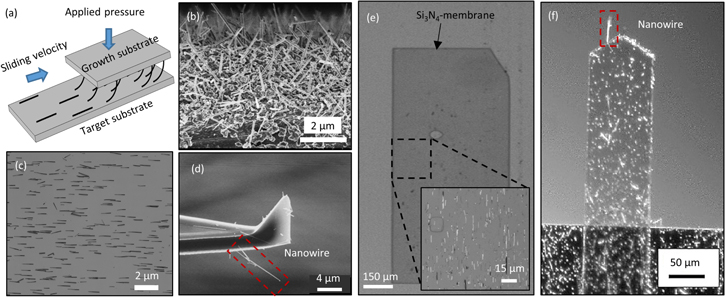
Figure 1. (a) Schematic of the contact printing process. The NWs are detached from the growth substrate as a result of applied pressure and sliding velocity and aligned on the target substrate. (b) Scanning electron microscopy image of SiNWs grown by VLS technique. (c) Laser scanning microscopy image of transferred SiNWs on a silicon chip. (d) Scanning electron microscopy image of printed NWs on a Si3N4-cantilever. (e) Light microscopy image of selective contact printing on a low-stress LPCVD Si3N4-membrane film with a thickness of 1 μm. The image insight image shows a closer view of printed NWs. (f) Scanning electron microscopy image of NWs printed on a Si-cantilevers with pyramidal tips.
Download figure:
Standard image High-resolution imageWhen the pressure or load applied during CP exceeds the NWs ability to withstand the mechanical bending stress, typically referred to as the tensile strength, fracture and thus, detachment of the NW from the growth substrate and transfer to the target substrate occurs. While this is generally considered to be the reason for NW transfer, directional or angular deposition control on the target substrate is controlled by the shear direction [29–31]. Dynamic control of the overall printing pressure and the shear direction consequently allows localized and dynamically controllable deposition of NWs with varying density and angular alignment. This is the basis of our explored concept of pressure-controlled two-directional contact printing (PCCP). PCCP thus eliminates the need for any surface modifications prior to the printing process and any lubricants.
In our paper, we first discuss the theoretical basis of the proposed PCCP strategy through simulations employing mainly the finite element method. For the experimental proof-of-concept, a three-axis PCCP tool was built, as described in the following, capable of controlling the vertical force directly during contact printing while shearing the growth and target substrate in two horizontal directions. For the experimental realization of PCCP, we utilized silicon NWs (SiNWs) grown by means of an in-house built chemical-vapor-deposition tube furnace reactor as described elsewhere [32] using the well-established gold-catalyzed vapor–liquid–solid (VLS) technique [33, 34]. For the growth process, Si(100) substrate covered by a 5 nm thick gold catalyst layer was utilized. SiNWs were synthesized at a temperature of 550 ℃ and a working pressure of 10 mbar using gaseous monosilane (SiH4) in helium and hydrogen with a flow rate of 10 sccm and 80 sccm, respectively. The length of the grown NWs can be controlled directly by adjusting the process growth time. NWs with a length in the range of 1–12 μm were grown within a growth time ranging from 30 to 90 min. On the other hand, the NW diameter depends strongly on the Au droplet size, which originates here from the de-wetting of the catalyst gold film. Accordingly, the NWs diameter in this work are in the range of 50–150 nm. Using the PCCP approach, the density, angle, and length distribution of printed SiNWs were controlled by adjusting the applied pressure and shear direction during printing. No lubricants or patterned resist layers were employed.
Both CP and PCCP are in principle compatible with different NW materials without restriction of length and diameter and can also be realized on different substrate materials. These aspects are very valuable for building heterogeneous micro- and nanodevices and make PCCP a versatile tool and a promising extension in the framework of CP NW transfer techniques. Selected application examples from our own research are shown in appropriate support of this technological potential, including the CP transfer of silicon NWs on freestanding microcantilever beams and flexible membranes (figures 1(c), (d)) as described further elsewhere [35]. With PCCP, we want to add another degree of freedom in this respect.
2. Contact printing analysis
To elucidate the impact of a dynamically applied pressure on CP, the transfer mechanisms of NWs need to be first discussed. In this regard, it is worth mentioning that the applied printing force is distributed to the NW assembly as a function of the NW number, length and overall arrangement. Hence, a certain loss of NWs during printing will consequently result in a change of the load for the remaining NWs, which can also be balanced by adequately adjusting the printing pressure during CP. Nevertheless, the applied printing pressure or force is only acting as effective pressure or force on a single NW. Understanding the behavior of single NWs during PCCP requires to model and acknowledge the NW bending behavior due to solid-state mechanics [36]. NWs are here considered as bending beams with cylindrical cross-sections that are fixed on one side to the growth substrate and in contact with the target substrate surface on the opposing end. When the applied effective pressure increases and the friction between the NW tip and surface is sufficiently high to prevent the displacement of the NW, a reaction is formed to oppose the deflection and return the NW to its stable form. This reaction causes bending stress, here labeled with σ, which is equal to


M denotes the bending moment in which P is the applied pressure and x is the length of the NW, y is the distance from the neutral axis, which is here in the center of NW cross-section, I is the second moment of area (here considered as a circular cross-section) in which R represents the radius of NW cross-section. Accordingly, it applies that the bending stress is linearly related to the applied pressure and the NW length, while a reciprocal relationship exists with the diameter of the NW. The linear relationships allow rational mechanical stress and, thus, in principle NW breakage control through appropriate pressure adjustment during contact printing. To elucidate the three-dimensional deformation state of NWs while considering various load scenarios, NW geometries and the frictional interaction between NW tip and the target surface, finite element method-based simulations were employed using the software COMSOL Multiphysics.
CP can in principle be implemented for different types of NWs, as mentioned before, that have different mechanical stability, lengths, and elastic properties, as long as sufficient friction or shear force can be generated and as long as the NWs break at a defined fracture point (typically at the base). The following simulation parameters were adjusted to our experimental results with respect to SiNWs. First, we study single NWs with a representative length and diameter of 1 μm and 50 nm, respectively being in contact with the target substrate under three different applied pressures. The respective movement of the NW base in Z and X-direction simultaneously yields in the applied pressure modeling. The required material properties of the NW are adjusted to represent [100] oriented single-crystalline silicon NWs with a tensile strength of 9 GPa [37]. In addition, the elastic modulus of SiNWs is considered to be 170 GPa, which corresponds to an average value of [100] Si in the bulk measured in the range of 130–180 GPa [38–40].
For modeling the friction between the NW and the target substrate, a spring model is assumed at the contact point of the NW and the target surface that opposes the NW movement. By applying pressure and sliding the NW on the surface, the produced stress inside the NW increases until reaching the maximum tolerable value equal to its tensile strength (i.e. here set to 9 GPa). Then the NW breaks and is transferred in the shear direction to the target substrate.
The different applied pressures are modeled by changing the NW base displacement in the Z and X-direction while they are in direct relationship. These pressures are considered 'High' in which the base displacement in Z is equal to X, 'Middle' in which it is equal to ½ of X and 'Low' in which it is equal to ¼ of X. The bending of the NWs under a 'High' and 'Low' applied pressure is shown in figures 2(a) and (b) and the resulting maximum stress is indicated on the NW. In case of a high-pressure regime, the NW breaks due to increased stress level inside it after movement of the NW base in X-direction (D) of about 0.07 μm. Moreover, the maximum stress is produced 0.6 μm away from its base, which results in NW fracture into pieces having a smaller length than the original NW. On the other hand, for low applied pressures, the bending stress increases to about 4.8 μN for a displacement D of 0.19 μm that is insufficient to trigger any breakage of the NW. Hence, after its buckling, the stress decreases and the NW starts to slide on the surface without getting detached from the growth substrate. However, after a displacement D of about 0.37 μm, the bending stress again increases. This is because of the friction between the NW and target substrate surface, which opposes the NW sliding. When reaching the maximum tensile strength of the NW (i.e. 9 GPa), the NW will break at its base and thus, the entire NW (i.e. 1 μm length) is being transferred from the growth to the target substrate. The bending stress graph of NWs under these three applied pressure is shown in figure 2(c).
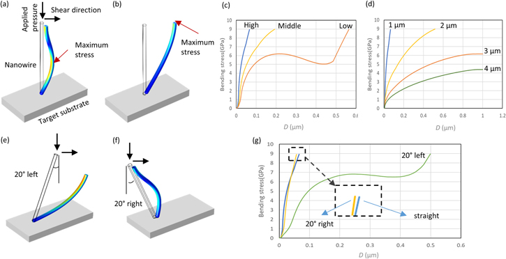
Figure 2. Schematic of a single NW in contact with target substrate under (a) 'High' and (b) 'Low' applied pressures. The graph of bending stress (GPa) versus shear displacement (μm) (c) for different applied pressures, and (d) for different lengths of NWs. Schematic of a NW with the length of 1 μm and diameter of 50 nm under a moderate applied pressure and tilted with an angle of 20° (e) toward and (f) opposite the shear direction. (g) The graph of bending stress (GP) versus shear displacement denoted as 'D' (μm) for straight and tilted NWs.
Download figure:
Standard image High-resolution imageAs mentioned, the length of NWs directly affects the mechanical behavior and, thus, the NW CP results. Accordingly, deformation of NWs with the length of 1–4 μm is modeled under the same applied pressure that is equal to the 'High' pressure mentioned in the previous part, and NW base displacement in X-direction (D) of 1 μm. The bending stress graph in dependence on the base displacement and NW length is shown in figure 2(d). It is observed that for NWs having a length of 1 μm and 2 μm, the maximum value of the bending stress (i.e. 9 GPa) is achieved after a short base displacement (i.e. 0.07 μm and 0.50 μm respectively). In comparison, for NWs with a length of 3 and 4 μm, the maximum bending stress is not reached using the same applied pressure and base displacement.
NWs synthesized by VLS growth without any epitaxial relationship to the substrate do not necessarily grow in a straight manner along the normal direction of the substrate surface but exhibit an axial alignment angle that deviates from the normal direction of the respective growth substrate surface. This will clearly affect the loading situation. Thus, the produced bending stress during the CP process will change and consequently, the transferred NW density and NW length distribution are altered. We addressed this issue in an approximation by considering a simple angular deviation from the normal direction of the substrate surface (shear displacement). The NWs were thus modeled with a deviation angle of 20°. It is furthermore essential to consider the shear direction with respect to the angle, which created two principles cased of a unidirectional shear movement: (1) tilted towards and (2) tilted against the shear direction as illustrated in figures 2(e) and (f) respectively. The comparison of the produced bending stress in these tilted NWs with the aforementioned vertically aligned NWs was examined under the 'High' pressure regime. The results show that NWs tilted against the direction of shear displacement oppose the bending of the NW, which results in breakage of the NW at the lower base displacement (D), i.e. 0.06 μm, in comparison to the straight NW. This is shown in the magnified part of the graph in figure 2(g). In addition, NWs tilted towards the shear direction under the same pressure breaks after a significantly larger base displacement (D), i.e. 0.52 μm and the behavior is similar to a straight NW under 'Low' pressure.
The simulations evidently demonstrate the role, need and benefit of controlling the applied pressure acting on the NWs during the CP process for a controlled assembly and serve as the basis for the PCCP approach. For the experimental realization of PCCP, an in-house three-axis PCCP tool was built, as described in the following, enabling distinct control of the density and angular alignment of the transferred NWs on the target substrate.
3. PCCP system
An in-house built PCCP system was used in this work consisting of two stages (Physik Instrumente GmbH & Co) that are horizontally aligned to enable a two-directional movement of the target substrate in the X and Y direction relative to the NW growth substrate that is mounted on a vertical axis. The vertical stage enables, besides a pure movement, the creation of a force and thus the creation of a pressure, which is equal to the force over the area that the force is applied. The printing parameters include the desired pplied pressure on the growth substrate, the directional movement of the horizontal stages, their displacement, and their velocities. The printing process itself using the set parameters is controlled by a self-written MATLAB code interface. To avoid any impact from changing humidity, temperature fluctuations and particles, the PCCP system has been installed in a cleanroom environment.
The two horizontal precision linear stages (L-590) that resemble X–Y stages are compatible with mm-size chips to 4' wafers with a travel range of 100 mm. The linear stages are equipped with a 2-phase stepper motor to produce a velocity of up to 20 mm s−1 and a ball screw for the smooth running of stages with unidirectional repeatability of 0.1 μm. The X–Y stages are controlled by a C-663.12 Mercury Stepper Motor Controller from PI, which records operating data including velocity and position and errors happening due to moving of stages out of rage with a cycle time of 50 μs. The holder of the horizontal stages is able to move the target substrate with the maximum diameter of 100 mm in a movement surface area of 100 × 100 mm2, as shown in figure 3(b). The substrate size can be selected comparatively flexibly within this framework, whereby even small target substrates down to a few square millimeters can still be installed. However, for better positional stability or reproducibility of the results, special holders or adapters are recommended in such cases in order to achieve an overall larger support surface.
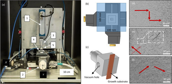
Figure 3. (a) Photographic image of the PCCP system consisting of a stage in the vertical arrangement (1) and two stages (2) in rectangular, horizontal (in-plane) arrangement (X and Y directions), a force sensor (3), the target substrate holder (4), and the growth substrate (5). (b) Schematic of the horizontal stages with an in-plane travel range of 100 × 100 mm2. (c) Schematic of the vertical stage holder with an illustrated growth substrate. (d) Dynamically changed NW density during the printing process by increasing the applied pressure (the red arrows indicate the increase in the pressure by moving the growth substrate more toward the target substrate). (e) Crossed arrangement of NWs by changing the printing direction (the red arrows present the printing layers and direction). (f) Changed alignment direction of NWs on the target substrate by utilizing two-directional printing (the red arrows show the printing direction).
Download figure:
Standard image High-resolution imageThe vertical voice coil linear actuator (V-273 PIMag®) can, as mentioned before, create a force or pressure acting on the target substrate after reaching mechanical contact with the growth substrate. Its magnetic motor is suitable for traveling with a high resolution of 0.01 μm and a velocity of 100 mm s−1 at a limited travel range of 20 mm. Moreover, the applied pressure can be adjusted by a mounted force sensor with a maximum value of 6 N and a resolution of 1 mN. The C-413 PIMag® Motion Controller is connected to this stage to read the force and position simultaneously and adjust the force with a defined holding or feed value. The holder of the vertical stage is currently designed to host substrates with an approximate size of 3 × 15 mm2 (figure 3(c)). If smaller growth substrates are required, for instance to minimize the printing area, other holders can be in principle designed and installed.
After loading the growth and target substrate to the stages and initiating the printing process, the vertical stage approaches the growth substrate to the target substrate until mechanical contact is formed and continues until the desired applied pressure is reached. The applied pressure created by the vertical stage displacement is measured at an average step size of 5 μm and it can be dynamically adjusted even during the CP process. After the printing pressure is set, the horizontal stages move the target substrate along a predefined printing velocity and X–Y printing path.
One of the most important features of this system is the ability to control the applied pressure dynamically during the printing process. Based on the basic idea of friction, where the frictional force is proportional to the acting normal force, localized control over the deposition density of NWs is immediately gained by this feature. Thus, it omits the need for any predefined surface structures to modify the friction locally. As shown in figure 3(d), by increasing the applied pressure from 0 to 4 N cm−2, the density of transferred NWs increases significantly in the respective area along the printing path, as expected. Another important feature of the PCCP tool is the possibility to create a two-directional movement based on the horizontal stages in the X and Y direction. Due to the fact that NWs will align in the shear direction, control of the angular alignment of NWs on the surface is directly provided. As shown in figures 3(e) and (f) the angular characteristics of the NW deposition follows clearly the stage travel path. Hence, cross-assembly and shaping of NWs on the surface are possible.
To further demonstrate the capability of the PCCP system to control the overall assembly and angular alignment of NWs in the CP process, a series of printing experiments were performed and the resulting laser scanning microscopy (LSM) images were analyzed.
4. Contact printing statistics
To improve the understanding of the effect of the applied pressure on the PCCP NW printing results, one-directional printings were performed. Within the experiments, the applied pressures were set at 2, 4, and 6 N cm−2 using a constant velocity of 2 mm s−1 for all pressures. The results were statistically analyzed for NW-to-NW spacing, NW density, length, and angular misalignment with respect to the shear direction.
The NW density can be non-uniform along the printing area, especially at the start and end of the printing process, until a steady movement is achieved or maintained. Consequently, we split each printing area, which is approximately 15 × 15 mm2 into three parts labeled 'Begin', 'Middle' and 'End' of the PCCP with roughly distance of 3 mm from edges of the printing area, as shown in figure 4(a). Each part was analyzed based on LSM images of three random spots with the size of 0.131 × 0.131 mm2, arranged with an approximate equal distance of 3 mm along the Y-axis. MountainsLab Premium software and a self-written MATLAB code were used for image processing and image data analyzing.

Figure 4. (a) Photographic image of a target substrate with deposited NWs (the bright layer is the transferred NWs) and the imaging pattern is indicated with numbers from 1 to 9. (b) Example LSM illustrations of the nanowire patterns in the three areas 'Begin', 'Middle' and 'End'. (c) and (d) Density (particles μm−2) × 103 and NW-to-NW spacing (μm) versus applied pressure (2, 4 and 6 N cm−2). (e)–(j) Histograms in dependence on the growth time (30, 60 and 90 min) based on a used printing pressure of 2 N cm−2 and a velocity of 2 mm s−1 with respect to NW length (μm) (e)–(g) and the NW deposition angle (°) (h)–(j).
Download figure:
Standard image High-resolution image
First, the densities of the printed NWs using an applied pressure of 2, 4, and 6 N cm−2 are compared in three aformentioned areas of the substrate surface (figure 4(c)). The graphs shows that the density of NWs is decreased from the area 'Begin' to the 'End' of the substrate for each applied pressure. For instance, in the case of an applied pressure of 4 N cm−2, the density is decreased from about 2.5 × 10³ to 1.1 × 10³ particles μm−2 across the printing area of NWs. Moreover, for each part of the substrate, i.e. 'Begin', 'Middle' and 'End', increasing of the applied pressure results in an enhanced breakage of NWs from the growth substrate yielding consequently, more NWs transfer to the target substrate that leads to a higher density of printed NWs as discussed earlier in the simulation part. However, this result is more visible for the beginning of the sample as the density of printed NWs has an increase from 1.8 × 10³ to 4.3 × 10³ particles μm−2 that is drastically higher than the end of the sample with the increase of only 0.05 × 10³ particles μm−2. NW-to-NW spacing, however, has a reverse relation with the density of printed NWs. It means that by increasing the applied pressure from 2 to 6 N cm−2, the distance between single NWs decreases, as can be seen in figure 4(d) (e.g. from about 20.4 to 10.7 μm for the 'Begin' of the printing area).
Furthermore, the distribution of length and angle of printed NWs using growth substrates with different growth times of 30, 60 and 90 min are compared in the 'Begin' of the substrate under an applied pressure of 2 N m −2. Before the CP process, the approximate length of NWs on these three substrates is measured by analyzing their scanning electron microscopy (SEM) images (figure 4(a)). The results indicate that for the growth time of 30, 60 and 90 min, the length of NWs is respectively in the range of 1 to 3, 1 to 6 and 1 to 8 μm. However, some random NWs are still observed being about 1–2 μm longer in length. The resulting histograms of NWs length after CP, as shown in figures 4(e)–(g), show a considerable distribution in the printed NW length as observed in the corresponding growth substrate. The high number of NWs in the range of 1–2 μm can originate from undesired breakage of the NWs. However, for NWs grown for 60 and 90 min, the distribution of printed NWs with their corresponding length from the growth substrate is more consistent. This can be due to the decreasing of the bending stress inside the longer NWs, which was explained in the simulation part.
In addition, we observed a high uniformity in the transferred NWs length throughout the printing area due to reasonable control over the constancy of the applied pressure in the PCCP tool. For instance, the average length of printed NWs that were transferred from a substrate with a growth time of 30 min under an applied pressure of 2 N cm−2 is about 2, 1.7, and 1.5 μm in the 'Begin', 'Middle', and 'End' of the substrate, respectively.
High control over the angular alignment of NWs can also be achieved by using the PCCP tool as shown in the angle histograms of printed NWs as shown in figures 4(h)–(j). Accordingly, a mean alignment angle of less than 10° is observed throughout the printing area and for NWs with growth times of 60 and 90 min, the angle is in the range between 0° and 5°, which is highly comparable with the results achieved by Christou et al being in the range of 5° of the sliding direction [28]. It can be hence concluded that the maximum stress required for breaking the short NWs (e.g. 1–2 μm) is achieved shortly after applying the pressure, which is not sufficient to change the direction of the NWs into the sliding direction and results thus in a certain degree of misalignment of NWs on the surface. Longer NWs (e.g. > 3 μm) require higher bending stress for breaking, which enables them to slide more easily on the surface until the contact friction creates the necessary stress for the breakage of the NWs as confirmed by the simulation results as well. The influence of the growth direction of the NWs on the growth substrate should therefore not be ignored during the CP process as it can directly have an effect on the produced stress inside the NWs (shown in the simulation part as well) and consequently make a difference to the alignment of the printed NWs.
5. Conclusion
In this work, we introduced the PCCP concept, which is based on dynamically controlling the applied pressure and shear direction during the CP process to directly influence the assembly characteristics, such as NW density and angular alignment, on a target substrate without utilizing pre- and post-preparation steps. In support of this concept, the mechanical behavior of straight and tilted NWs with varying lengths and under various applied pressures was analyzed by finite element modeling. The results represent the effect of grown NW length and deviation angle on the produced bending stress inside the NW and consequently the printing results.
For the proof-of-concept, a two-directional PCCP tool was built to transfer NWs from the growth substrate to the target substrate with a high control precision. In principle, this system can handle various kinds of NWs and substrate materials. The tool performance was evaluated by using different printing pressures and analyzing the density, length, and spacing of the printed NW assemblies. The results indicate that increasing the applied pressure increases the density of NWs but decreases their average spacing. Moreover, a higher degree of uniformity on the target substrate can be observed in terms of NWs length and alignment angles for printed NWs with longer growth lengths. Based on these results, we demonstrated that the PCCP concept appears to be a valuable addition to the scope of CP techniques. Nevertheless, further studies and control within PCCP are required to push the current limits of this technology towards lateral single-nanowire control.
Acknowledgments
The authors gratefully acknowledge the financial support by the Deutsche Forschungsgemeinschaft (DFG, project number: 392124230) and the German Federal Ministry of Education and Research (BMBF, NanoMatFutur 13N12545) as well as the experimental support by S. Jenisch, R. Ehrlich, A Schreiber (Ulm University), and Mohamad Akkad, A. Albrecht, and from the entire ZMN and MST team (Technische Universität Ilmenau).
Data availability statement
All data that support the findings of this study are included within the article (and any supplementary files).