
Abstract
Single hole transport and spin detection is achievable in standard p-type silicon transistors owing to the strong orbital quantization of disorder based quantum dots. Through the use of the well acting as a pseudo-gate, we discover the formation of a double-quantum dot system exhibiting Pauli spin-blockade and investigate the magnetic field dependence of the leakage current. This enables attributes that are key to hole spin state control to be determined, where we calculate a tunnel coupling tc of 57 μeV and a short spin−orbit length lSO of 250 nm. The demonstrated strong spin−orbit interaction at the interface when using disorder based quantum dots supports electric-field mediated control. These results provide further motivation that a readily scalable platform such as industry standard silicon technology can be used to investigate interactions which are useful for quantum information processing.
Export citation and abstract BibTeX RIS

Original content from this work may be used under the terms of the Creative Commons Attribution 4.0 licence. Any further distribution of this work must maintain attribution to the author(s) and the title of the work, journal citation and DOI.
1. Introduction
Silicon (Si) based devices have become the cornerstone of modern technology, and are now a leading candidate for quantum information processing architectures [1–4]. Promising alternatives to traditional metal-oxide-semiconductor field-effect transistors (MOSFETs) take the form of quantum dots (QDs) as qubits in single electron devices through the use of charge and spin as the fundamental building blocks [5–7]. The use of multi-gate device architectures in particular has led to many breakthroughs by tuning the potential profiles defining QDs as well as the inter-dot tunneling barriers for precise control, where development is undertaken by academia and large pre-industrial fabrication facilities [8–14]. Using Si for spin based quantum computing regimes is a natural choice for not only scalability and ease of integration with industrial fabrication techniques, but also long coherence times owing to isotopically enriched zero nuclear spin 28Si [15, 16]. The feasibility of spin qubits has also been demonstrated by high fidelitys exceeding 99.8%, which can be utilized in combination with quantum error correction towards achieving fault tolerant quantum computing, promoting spin as a competitive candidate in this space with respect to trapped ion and superconducting platforms [17–21].
Efforts have also been made to take advantage of features already present at the single electron level in Si VLSI technology. The use of trap states within Si quantum devices can complement and even enhance single charge transport, with applications ranging from quantum information and quantum metrology, to bio-sensing and hardware security [22–25]. In quantum metrology, record high frequency benchmarking for single electron pump operation was achieved as a consequence of a coupling between a QD and trap state, yielding improved operation for establishing a new current standard [26, 27]. In addition, hole spin resonance of trap states within a p-type MOSFET was achieved using Pauli spin-blockade (PSB) to study spin−orbit (SO) state mixing [28].
Alongside scalability, another technological obstacle to overcome is that of electric-field mediated control, which relies on a strong SO interaction, but in the case of electrons in Si is intrinsically weak [29–31]. This has given rise to investigations into transport schemes with an enhanced SO interaction, where attempts using holes, valley states and the inversion asymmetry at the oxide interface has led to strong SO effects [32–36]. PSB, a common measurement tool used throughout quantum information protocols, is also dependant on the SO interaction when detecting spin states [37–43]. This is manifested as the suppression of current through a double-QD system in a triplet state as a consequence of the Pauli exclusion principle. Such a technique effectively allows individual spins to be read by correlating the spin state with the charge state through monitoring the double-QD current [44, 45]. Within this regime, singlet−triplet (S−T) state mixing, relaxation mechanisms, and SO coupling can be probed, since the SO interaction offers a mechanism for coupling hole spin with their orbital motion.
In this work, we investigate the coupling and SO interaction of disorder based states present in p-type Si MOSFETs through PSB, achieved via tuning gate and well voltage to form a double-QD. This allows the determination of the tunnel coupling (tc ) and SO length (lSO), which offers a direct measure of the SO interaction strength and therefore a method to evaluate the potential of a given system for electric-field mediated control, as well as high frequency spin manipulation. As a result, we take advantage standard Si transistors to find enhanced SO effects of disorder QDs at the oxide interface and obtain a lSO much shorter than anticipated using Si QDs.
2. Methodology
A schematic of the Si p-type MOSFET sample measured is displayed in figure 1(a), with a 2.4 nm thick SiON gate dielectric and a highly doped poly-Si gate with a channel length/width of 120 nm and 500 nm respectively. As the channel becomes inverted a 2 dimensional hole-gas (2DHG) begins to form and single charging characteristics from QDs can be observed due to quantum confinement. In our device, this is a consequence of surface edge roughness by poly-Si grains in the gate and traps at, or close to the Si-oxide interface based on the charging properties observed, as depicted in figure 1(b) [46–49]. Typically temperatures below 4 K are sufficient to observe single hole tunneling due to discrete energy levels in such QDs. All measurements here were carried out within an Oxford instruments 4He cryostat at a temperature of 1.6 K.

Figure 1. (a) Schematic of p-type Si MOSFET sample with channel dimensions 500 nm width and 120 nm length. (b) Cross-section of device displaying disorder at the Si-oxide interface leading to a 2DHG forming below defects. (c) Energy level diagram showing valance band bending which leads to double-QD formation and the conditions for PSB.
Download figure:
Standard image High-resolution imageOur method to electrically characterize QDs is via I−V characteristics using Yokogawa source meters. This is achieved through biasing the gate ( ) and source (
 ) terminals while measuring current from a grounded drain terminal (
 ), to generate a charge stability diagram (CSD). Coulomb diamonds (CDs) appear as a result of Coulomb blockade (CB) in the sub-threshold region, whereby transport is blocked due to the electrostatic energy and level splitting of holes occupying the QD, which can be lifted by the capacitively coupled gate and source terminals. This not only allows information on the size and couplings of QDs to be calculated, but also the presence of multiple CDs overlapping highlight double-QD transport features, a key requirement for PSB (figure 1(c)) in order to study SO effects. We use a p-type MOSFET in particular to take advantage of the enhanced SO interaction of valance bane holes, owing to their p-orbital nature [33].
3. Results and discussion
The resulting CSDs are displayed in figure 2, where differential conductance ( ) is plotted to aid in highlighting finer features outside CB, including excited states, and most importantly, to better visualize PSB. This method is more effective than plotting current, where the magnitude can vary as a result of offsets from both triplet leakage and parasitic current paths through the channel. The experimental data is plotted in figures 2(a)–(c), with simplified CSDs drawn in figures 2(d)–(f) to better visualize the significant changes. CB appears as blue in figures 2(a)–(c), with red denoting high
  due to the availability of levels for single hole transport. Amplifier current saturation occurred at 1.3 nA producing blue regions at high
  and
and  . Each CD, corresponding to blockaded transport within the QD system, are marked by a letter and number in figures 2(d)–(f). A well voltage (
 ) of 1 V is applied in figure 2(d), and a series of largely closed CDs are observed. This suggests that transport is occurring through a single QD, where we interpret CDs A1−C1 from QD2, and CD D1 from QD1. The energy band diagram (EBD) depicting this situation is shown in figure 2(g) for the region marked by the star in figure 2(d). Due to the small size of the CDs B1 and C1 in figure 2(d), single QD transport can occur as a consequence of a reduction in tunneling barrier distance between the source and drain due to the larger QD size, shown schematically in the valence band diagram in figure 2(g).
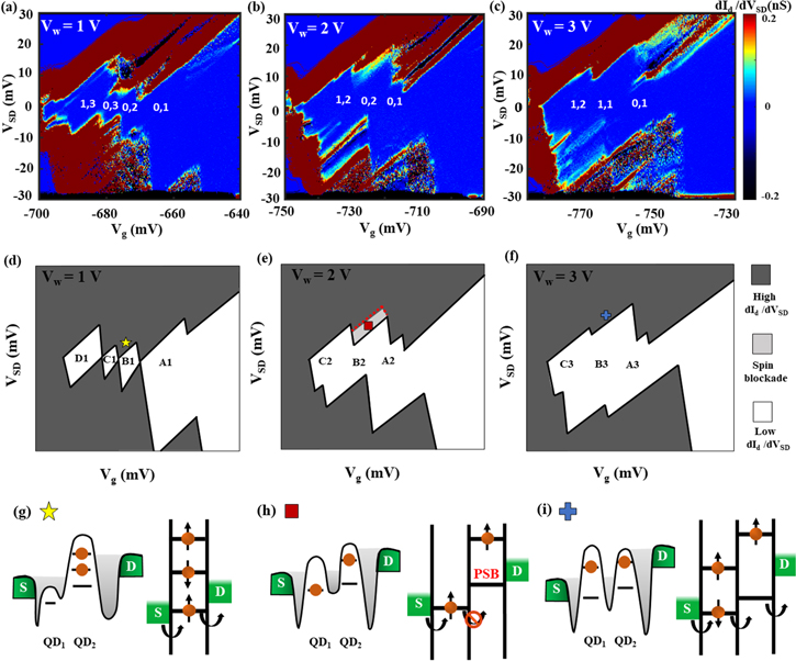
Figure 2. Charge stability diagrams (CSDs) for  = −30 to 30 mV over a 60 mV gate voltage (
 ) range at different well voltages (
 ). Within the Coulomb diamonds (CDs) the number of confined holes in each QD (QD1, QD2) are labelled. (a)
  = 1 V, a row of single CDs appear with various charging energies. (b)
  = 2 V, the alignment of the QD energy levels change, resulting in overlapping of the CDs which strongly suggests double-QD transport. (c)
  = 3 V, the alignment of the CDs is further altered, leading to regions of extended Coulomb blockade. The confinement of an additional hole within the dominant transport path is marked by letters A, B, C and D in simplified CSDs (d)−(f), where the number refers to the
  magnitude, however the same letter does not necessarily denote the same QD energy level in each CSD. The appearance of a PSB like low
  region at the edge of B2 for positive
  is annotated in (e), where the absence is noted at the edge of B3 in (f) from a change in coupling between the confined levels. (g)−(i) show energy band diagrams marked by the star, square and cross in (d)−(f) respectively. At
  = 1 V the transport is assumed to occur largely through a single QD, upon increasing
  to 2 V the confinement changes (from larger CDs), together with the QDs becoming weakly coupled and form a double QD exhibiting PSB. When
  = 3 V the energy level alignment shifts between the double QD, removing PSB and allowing transport to occur.
Download figure:
Standard image High-resolution imageWhen  = 2 V in figure 2(b) the CSD changes significantly from the shift and overlap of CDs, in particular we note the appearance of a low
  region enclosed by the red dotted line outside of the CD B2 for positive
  in figure 2(e). This can be interpreted as an initial indicator of PSB, since the transport path will not be completed blockaded due to a slightly elevated Id
from triplet leakage that leads to a non-zero, low
in figure 2(e). This can be interpreted as an initial indicator of PSB, since the transport path will not be completed blockaded due to a slightly elevated Id
from triplet leakage that leads to a non-zero, low  . We find the optimum contrast is at a threshold of 0.05−0.1 nS to make the PSB region most visible. CB of the dominant transport path also expands considerably between figures 2(a)–(b), from the enhanced confinement of the smaller CDs observed in figure 2(d) as a result of the large scale changes. QD1 emerges from a partially joined potential profile in figures 2(g)–(h) which separates due to the application well voltage forming a tunneling barrier between the QDs as well as increasing the confinement of QD2. The valance band schematic given in figure 2(h) during PSB highlights the important changes leading to this result, such as the formation of a weakly coupled double QD through a modified tunneling barrier between them. The number of confined holes in each QD also now satisfies the conditions of PSB, due to the spin selective nature of the second hole entering QD2. Therefore a combination of both the appropriate number of confined holes and the extended region of low
  strongly suggests PSB. Upon increasing
  further to 3 V in figure 2(c) the CSD pattern, and therefore the dominate transport path, largely resembles that of figure 2(b) with the exception of the B2, which displays an extended CB and the absence of the unique low
  feature highlighted previously when comparing figures 2(e) and (f). This can be explained by the EBD and valance band schematic in figure 2(i) for the cross in figure 2(f). The energy level alignment shifts, allowing hole transport through the second level in both QDs. Along with changes to tunneling barriers and QD energy level alignment at higher
  values, a considerable threshold shift is also evident. This is explained by an increasing depletion layer width causing more positively charged ionized dopants to be exposed, and therefore requires a more negative gate voltage to compensate to achieve the same 2DHG formation.
Upon further analysis, the physical attributes of the dominant transport path are determined through estimating the dimensions of charge stable regions in figure 2 for positive  . This is achieved by calculating gate capacitance (
 ) and charging energy (
 ) according to
  and
and  [50], where e and
  are elementary charge and total capacitance respectively, as summarized in table 1.
  represents the energy required to add an additional hole to the QD and
  is associated with the strength of the coupling between a given confined level and the gate. Determining such values allows a greater understanding of the systems components and their relationship with respect to
  . Since Si dangling bonds have charging energies of 13 meV above the valence band we propose the origin of the confined levels where
  is close to 13 meV to be due to dangling bonds or trap sites at the oxide interface [51]. CDs with
  values less than this (such as B1 and C1) are assumed be generated by fine poly-Si grains. We estimate the QD diameter (
 ) from the QD surface area (SQD) and effective oxide thickness (teff) by
  , using
  and
and  , where
  is the permittivity of the oxide. Given this, we calculate the projected
  of the smaller CDs B1 and C1 in figure 2(a) to be ≈50nm. This further supports poly-Si grains as the confining potential origin given that fine poly-Si grain structures reach diameters of the order 50 nm [52]. Although the CSD pattern is similar when comparing figures 2(b) and (c), the highlighted region in figure 2(e) disappeared when
  = 3 V. As shown schematically in figure 2(h), the specific transport path in figure 2(b) was no longer available in figure 2(c). Such changes which lead to increases in
  and
and  further demonstrate that the response of each confined level varied according to
  , where the energy level alignment between the QDs shifted, together with the barrier height between them. This is also likely attributable to QD origin, since each QD will have a different capacitive coupling to
  , as with
  , depending on the location and size of the QD as the depletion layer changes [53]. The formation of QD2, as the likely product of a poly-Si grain, appears to be more susceptible to
  from the enlargement of CD B1 to B2 which we ascribe to the same origin, in comparison to the change of CD D1−C2 of QD1 from what is likely an interface trap given the
  .
.
Table 1. Single hole charging properties of CDs as labelled in figure 2.

| CD (No.) |

| Cg (aF) |
|---|---|---|---|
| 1 | A1 | 13.3 | 10.4 |
| 1 | B1 | 6.3 | 24.6 |
| 1 | C1 | 5.5 | 28.6 |
| 1 | D1 | 12.5 | 11.8 |
| 2 | A2 | 8.9 | 13.3 |
| 2 | B2 | 16.1 | 9.8 |
| 2 | C2 | 12.7 | 10.4 |
| 3 | A3 | 10.3 | 11.7 |
| 3 | B3 | 19.8 | 7.2 |
| 3 | C3 | 12.1 | 11.1 |
Focusing on the low  region in figure 2(e), a
  and
and  sweep at fixed
  is shown in figures 3(a) and (b) respectively. The
  valleys in figure 3 denote CB, whereas the marginally elevated
  plateaus correspond to PSB. A dip in current at
  signifies the profile sweep nearing a CD edge, although the system does not enter CB. Figures 3(c)–(f) show EBDs for the regions labelled by the star, square, circle and cross in figures 3(a) and (b). These visually demonstrate how the transport scheme is altered through the application of
  and
and  . For the star marked in figure 3(a), an EBD in figure 3(c) shows the system entering CB due to the absence of a level for the first QD. In figure 3(d), at larger
  a level becomes available, but transport is blocked between the QDs due to Pauli selection rules. PSB is temporarily lifted at higher
  due to the lowering of a level for QD1 within the transport window, however CB then occurs as displayed in figure 3(e) due to a level dropping above the drain for QD2 (circle). An EBD is also given for the CB region preceding PSB at lower
  (cross) in figure 3(f). While an
  leakage current of 4 pA is observed in the CB region due to parasitic current paths in the channel, an
  of 5.6 pA within the PSB region suggests the triplet leakage is 1.6 pA, which is comparable to similar devices exhibiting PSB [31, 40, 41].
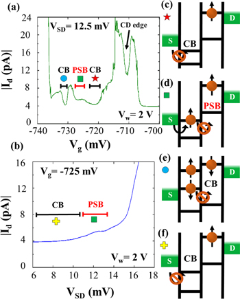
Figure 3. For  fixed at 2 V, a gate sweep with
  = 12.5 mV is shown in (a), and a source sweep with
  = −725 mV is displayed in (b). Coulomb blockade (CB), together with the suspected Pauli spin blockade (PSB) region from low
  are labelled. (c)−(e) show energy band diagrams marked by the star, square and circle in (a) corresponding to the CB regions as well as PSB. In (f), an energy band diagram for CB conditions marked by the cross in (b) is displayed, where PSB then occurs at higher
  .
.
Download figure:
Standard image High-resolution imageFurther to the  leakage measurements suggesting that the system is in a PSB configuration, much more tangible evidence can be obtained by investigating the magnetic field dependence, offering a window into the prevailing mechanism and any resulting spin related phenomena. Figure 4(a) shows a higher resolution CSD generated to identify the PSB region clearly. We focus on the area within the white dashed-circle in figure 4(a) and apply a magnetic field parallel to the channel to investigate spin transport relating to PSB, where a parallel field is applied to minimize orbital effects [28]. Figure 4(b) shows
  as a function of B-field from −2 to 2 T for
  = −715 to −725 mV along the pink dashed line in figure 4(a). Two peaks become visible at ±0.5 T due to an elevation in
  from around 10 to 15 pA. A higher resolution B-field sweep from 0 to 1 T is displayed in figure 4(c). Here the
  peak centered around 0.5 T can be observed to extend over a Vg
region of approximately −723.5 to −727.5 mV (marked by red arrow), which closely matches the voltage space dimensions of the low
peak centered around 0.5 T can be observed to extend over a Vg
region of approximately −723.5 to −727.5 mV (marked by red arrow), which closely matches the voltage space dimensions of the low  in figure 4(a). The resulting magnetic field dependant peaks appear due to different relaxation processes competing with each other from a combination of both the SO interaction and the Zeeman effect on account of the applied magnetic field, where the latter becomes more efficient at higher fields and therefore allows transitions between singlet (S) and triplet (T) configurations [31]. Based on this, the peaks at a finite field are explained by the lifting of PSB as a result of strong SO induced S−T mixing [32]. In figures 4(d)–(e) energy level diagrams are displayed, where (
 ,
, ) refers to the number of holes in the highest occupied orbitals of
  and
and  . In the absence of a magnetic field only the S(1,1) state can provide a direct route to S(0,2) which are tunnel coupled by tc
, and PSB occurs if the system enters the T(1,1) state (figure 4(d)). The blocked T(1,1) states with parallel spins can be lifted however by both relaxation to the S(1,1) state and S(0,2) through mixing on account of the SO interaction introducing non spin-conserving tunneling between the QDs. When a magnetic field is applied the blocked triplet states are split by the Zeeman energy which effectively alters the relaxation rate by providing faster alternative routes between the T(1,1) and S(0,2) mixed states and leads to an increase in Id
leakage (figure 4(e)).
. In the absence of a magnetic field only the S(1,1) state can provide a direct route to S(0,2) which are tunnel coupled by tc
, and PSB occurs if the system enters the T(1,1) state (figure 4(d)). The blocked T(1,1) states with parallel spins can be lifted however by both relaxation to the S(1,1) state and S(0,2) through mixing on account of the SO interaction introducing non spin-conserving tunneling between the QDs. When a magnetic field is applied the blocked triplet states are split by the Zeeman energy which effectively alters the relaxation rate by providing faster alternative routes between the T(1,1) and S(0,2) mixed states and leads to an increase in Id
leakage (figure 4(e)).

Figure 4. (a) Charge stability diagram for  = 0 to 20 mV and
  = −705 to −740 mV with
  = 2 V at the edge of a Coulomb diamond (white), where a reduction in current was observed due to blockaded transport through the two QDs. (b) Current as a function of magnetic field in the PSB region at fixed
  = 15 mV between
  = −715 and −725 mV (pink dashed line in (a)), two peaks are present due to an increase in the PSB leakage current at 0.5 T. (c) High resolution magnetic field spectroscopy scan with a clearly identifiable peak, where the extent of the maximum magnetic field enhanced spin relaxation current with respect to Vg
is indicated by the red arrow. (d) Energy level diagrams for PSB occurring in a double QD, where the path to S(0, 2) is blocked due to parallel spins in each QD, and (e) where the blockade is partially lifted due to enhanced relaxation from S−T mixing when a finite magnetic field is applied.
= −715 and −725 mV (pink dashed line in (a)), two peaks are present due to an increase in the PSB leakage current at 0.5 T. (c) High resolution magnetic field spectroscopy scan with a clearly identifiable peak, where the extent of the maximum magnetic field enhanced spin relaxation current with respect to Vg
is indicated by the red arrow. (d) Energy level diagrams for PSB occurring in a double QD, where the path to S(0, 2) is blocked due to parallel spins in each QD, and (e) where the blockade is partially lifted due to enhanced relaxation from S−T mixing when a finite magnetic field is applied.
Download figure:
Standard image High-resolution imageThe enhanced relaxation rate is mediated by the SO coupling and proportional to  , where alpha is a ratio characterizing the relative strength of tunnel and spin–orbit couplings tc
and tSO, and B is the applied field. As such this leads to significant changes when the enhanced leakage becomes comparable to
, where alpha is a ratio characterizing the relative strength of tunnel and spin–orbit couplings tc
and tSO, and B is the applied field. As such this leads to significant changes when the enhanced leakage becomes comparable to  , the average relaxation rate at zero field from (1,1) to S(2,0), and therefore a noticeable change in leakage
  due to the lifting of PSB becomes apparent. A model to describe the leakage
  due to this mechanism as detailed in [30] is given by the equation:
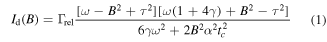
Here,  ,
,  (where Γ is the transfer rate from S(0,2) to the drain) and
  is the total coupling energy. To convert an applied magnetic field to the energy splitting; the Zeeman energy is calculated via
  , where
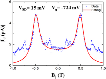
  is the Bohr magnetron and g is the gyro-magnetic ratio which we assume to be ≈2. We apply this theory in the form of fitting (red) to the data in figure 5, where a single point centered around the site of PSB at
  = −724 mV is plotted. A zero field dip can be noted, together with two clear leakage
  peaks at ±0.5 T with a magnitude of around 5 pA. As discussed earlier a parasitic current path elsewhere through the channel led to an additional current measured within CB, therefore we subtracted this offset, as well as the current from an isolated charge trap event, to produce a PSB leakage current of around 1.6 pA at zero field. With the combination of the known splitting energy and equation (1), we extract a tc
of 57
peaks at ±0.5 T with a magnitude of around 5 pA. As discussed earlier a parasitic current path elsewhere through the channel led to an additional current measured within CB, therefore we subtracted this offset, as well as the current from an isolated charge trap event, to produce a PSB leakage current of around 1.6 pA at zero field. With the combination of the known splitting energy and equation (1), we extract a tc
of 57  from the data, which is in good agreement for gate defined silicon QDs in a MOSFET device with similar dimensions [10]. Since α is a ratio that can be used to parametize the QD diameter to lSO, it enables a way to gauge the SO interaction strength relative to the confining potential, where lSO describes the ballistic distance travelled by a hole relative to its spin precession [41, 54]. Due to this, lSO is related to
  via
via  , which for a calculated
  of around 30nm using figure 2(e) gives an lSO value of 250 nm.
Figure 5. A profile plot showing the magnetic field dependant leakage current (blue) of a single point centered within the PSB region at a  of 15 mV and
  . Peaks begin to appear at ±0.5 T where a leakage current of around 5 pA is observed. Using equation (1) a fitting is applied to the peaks (red) to extract a tc
of 57 μeV and an lSO of 250 nm.
. Peaks begin to appear at ±0.5 T where a leakage current of around 5 pA is observed. Using equation (1) a fitting is applied to the peaks (red) to extract a tc
of 57 μeV and an lSO of 250 nm.
Download figure:
Standard image High-resolution image
Comparing the lSO obtained with others reported in Si reveals that our value is almost two orders of magnitude smaller than bulk Si, where 20 μm has been measured [55]. We also obtain a much lower value when compared to a Si spin qubit device with an lSO of 1 μm which was achieved using electron based QDs. Lengths as low as 110 nm have been estimated in Si but using heavy holes in a planar multi-gate defined QD device, operating at temperatures an order of magnitude smaller with reference to our MOSFET device [32, 34]. Generally speaking our results indicate that the lSO of Si disorder QDs characterized here are closer to those measured in III−IV materials which are typically ≈130–250nm [29, 41, 56]. It should be noted that single hole transport here is only possible owing to QD formation in such devices as a result of defects at the interface. Whether they are local to the gate, such as poly-Si grains and traps, or other impurities which create variable potential profile, are largely a natural consequence of stochastic processes. Although the inability to control the number of QDs in this type of system remains, the use of the well allowed control over the transport properties within a multi-level system which lead to the emergence of PSB. The creation of such a configuration yielded a relatively strong SO interaction given the lSO extracted. Such an effect has been previously attributed to inversion asymmetry at the interface possibly due to position dependent electric fields at the oxide boundary [34]. Therefore our results support engineering strong SO interactions at the interface in Si, as such we envisage more focus on exploring the useful properties of disorder QDs, particularly at the Si-oxide interface. This may well be of interest for industries where standard MOSFETs can act as a testing platform for quantum information processing schemes.
4. Conclusion
To conclude, pseudo control over the QD confinement potentials originating at the Si-oxide interface can be achieved as a consequence of well tuning to shift the energy level alignment and coupling between two QDs, allowing double QD transport phenomena to be probed in this type of system. This enabled spin related transport properties to be investigated through PSB, producing a significantly short lSO of 250 nm as well as a tc of 57 μeV. Our work therefore highlights a path for exploring alternative quantum information technologies using disorder based QDs by accommodating their advantageous SO properties at the interface on an accessible platform such as industry standard Si MOSFETs.
Acknowledgments
This work is supported by EPSRC Manufacturing Fellowship (EP/M008975/1) and Lloyds Register Foundation International Consortium of Nanotechnology.
Data availability statement
The data that support the findings of this study are openly available in Southampton ePrint research repository at:https://doi.org/10.5258/SOTON/D1485.