
Abstract
The growth of graphite on polycrystalline Ni by chemical vapor deposition (CVD) and the microstructural relation of the graphitic films and the metallic substrate continues to puzzle the scientific community. Here, we report the wafer-scale growth of a nanometer-thick graphite film (∼100 nm, NGF) on Ni foil via a fast-thermal CVD approach (5 min growth). Moreover, we shed light on how localized thickness variations of the NGF relate to the Ni surface topography and grain characteristics. While on a macro-scale (mm2), the NGF film looks uniform—with a few hundred highly ordered graphene layers (d0002 = 0.335 nm), when studied at the micro- and nano-scales, few-layer graphene sections can be identified. These are present at a density of 0.1%–3% areas in 100 µm2, can be as thin as two layers, and follow an epitaxial relation with the {111} fcc-Ni planes. Throughout the 50 cm2 NGF, the sharp graphite/substrate interfaces are either composed of a couple of NiCx layers or a graphene layer. Moreover, the NGF was successfully transferred on SiO2/Si substrate by a wet chemical etching method. The as-produced NGFs could complement or offer an alternative to the mm-thick films produced from natural graphite flakes or polymer sheets.
Export citation and abstract BibTeX RIS

Original content from this work may be used under the terms of the Creative Commons Attribution 4.0 license. Any further distribution of this work must maintain attribution to the author(s) and the title of the work, journal citation and DOI.
Highlights
- Grew wafer-scale (50 cm2) nanorange-thickness graphite thin films (∼100 nm, NGF) on polycrystalline Ni foil
- Discovered crucial parameters to control NGF thickness and uniformity (mm2 scale)
- Reduced significantly NGF growth step time (5 min) as compared to previously published approaches
- Explored and discussed fold formation on NGF surface associated with Ni surface topography
- Observed the epitaxial growth of FLG on Ni (111) grains mediated by a sharp interface of a single layer of C atoms via transmission electron microscopy (TEM)
1. Introduction
Graphite films have been used for a wide range of applications [1–4] such as heating elements in high temperature and high vacuum systems [5], fire retardant barriers [6], high temperature sealing gaskets [7], etc. For decades, commercial graphite films have been produced by processing of natural graphite flakes or polymer sheets [8–10]. When graphite flakes are used, these are intercalated, expanded, and then molded/sintered to form films [7], offering a low-cost production method. However, these films have poor electrical conductivity as a result of limited interlayer junction contacts and structural defects in the processed flakes. Improving the crystalline quality of these films often requires further graphitization steps (annealing at ∼2000 ºC–3000 ºC) [11–13]. Graphite films derived from polymers also show highly ordered layers after two key steps: (i) carbonization of the precursor film at 1400 ºC and (ii) graphitization at ≥3200 ºC [8, 10, 14–17]. These films are commercially available as mm-thick sheets [8, 10, 14]. However, this method consumes large amounts of energy and cannot make large-area graphite films with a thickness of less than a few microns [15].
Amongst the various synthesis methods, chemical vapor deposition (CVD) is consensually considered one of the most promising to obtain graphene with high crystalline quality at large-scale, whilst keeping reasonable production costs [18–25]. In the past two decades, most of the CVD research has focused on growing graphene and/or ultrathin graphite films (<10 nm). Unlike the significant success in achieving uniform monolayer graphene growth on Cu, obtaining reasonably uniform graphene/graphite film on Ni substrate is not so commonly observed in the literature [18, 23, 26]. Moreover, nanometer-thick graphite films (NGF), with a thickness ranging from 10 to 100 nm, have been overlooked [18–23]. Consequently, high-quality NGF is not available in the market. The use of a Ni substrate is suitable to grow these films due to the relatively high solubility and diffusivity of C in this transition metal (as compared to Cu, for instance) [19, 27, 28]. To date, the thermal CVD method has achieved some success in growing large area NGFs [2, 23, 29]. However, this method was used under conditions such as (i) single crystal Ni substrates, (ii) high growth temperature (>900 ºC–1300 ºC), (iii) longer growth time (several tens of minutes), (iv) low-pressure environment, (v) thick Ni foils, etc [2, 23, 29, 30]. As a result, costs to produce NGFs increase, thus limiting the use of CVD for large-scale production. Unfortunately, many of these reports provided minimal detail on thickness uniformity over a large area. Other approaches with lower process temperature (450 °C–700 °C) include the use of a plasma-enhanced CVD [31, 32]. However, plasma-based processes not only induce lattice defects but also generate amorphous carbon [31] and result in films with non-uniform thickness. In fact, controlling the NGF thickness over a large area remains a challenging task [15, 18, 33]. Additionally, detailed studies delving into the effect of the topography of host substrates on the NGF growth are scarce. Overall, understanding of the CVD growth mechanisms and how to obtain high-quality NGFs with controlled thickness from it are still limited.
Here, we report the preparation of high-quality NGFs with the following key aspects: (i) fast, wafer-scale CVD growth, with controlled nanorange thickness (∼100 nm) on polycrystalline Ni foils and (ii) structural studies to understand the effect of Ni surface topography on NGF growth, through detailed TEM measurements and analysis.
2. Experimental methods
2.1. NGF growth and transfer
A 25 µm Ni foil (99.5% purity, Goodfellow) was loaded into a commercial CVD reactor (4" BMPro Aixtron, figure SI1(a) (available online at stacks.iop.org/NANO/31/485605/mmedia)). The parameters profile is schematized in figure SI1(b). The system was purged with Ar and evacuated to 10–3 mbar. The Ni foil was then heated to 900 °C with a ramp rate of 75 °C min–1 in Ar/H2 (500/1000 sccm) while a chamber pressure of 10 mbar was maintained [20]. After the pre-annealing step of the Ni foil (5–30 min), the NGF was deposited by exposure of the foil to a CH4/H2 flow (100 sccm each) [20] at 10–500 mbar in the temperature range of 700 °C–900 °C and, for 1–45 min. Then, the sample was cooled down at a rate of 40 °C min–1, via an Ar flow (4000 sccm) [20]. The as-grown NGFs were transferred on SiO2/Si substrate and Cu grid with lacey carbon film by the use of an improved wet-chemical process, as described elsewhere [30, 34, 35].
2.2. Characterization techniques
Scanning electron microscopy (SEM) was performed by a Nano FEI Nova and a Zeiss Merlin (both at 1–5 kV, 50 pA). The sample surface roughness was measured via atomic force microscopy (AFM, Dimension Icon SPM, Bruker). For transmission electron microscopy (TEM) investigation, the cross-section lamella was prepared with a FEI Helios G4 focused ion beam (FIB) SEM microscope, equipped with a field emission gun and a Leica cryo-holder stage. To protect the region of interest, we coated the sample with a 5 nm layer of Ir and 1.5 µm of Pt. Then, the milling procedure was carried out, with the cryo-stage set at −145 °C and by the use of an ion beam of 16 kV (to reduce sample damage and artifacts formation) with a current range of 10 nA to 12 pA. Once completed, the thin lamella was slowly warmed up to room temperature. The cross-section TEM analysis was performed via a FEI Titan 80–300 Cubed microscope equipped with a high-brilliance field emission gun (300 kV), a Wien-type FEI monochromator and a CEOS spherical aberration corrector (for the objective lens) to allow a final spatial resolution of 0.09 nm. High-resolution TEM (HRTEM) images were acquired in low-dose conditions (10–20 electrons/Å2/second) with a Gatan K2 IS direct detection camera. A setting of a low-dose beam condition was necessary to preserve the fine structure of the sample. For the graphene layers to be imaged, the Ni crystallites of the foil were oriented along a proper zone axis to have the Ni (1 1 1)//NGF (0 0 0 2) interface parallel to the electron beam. Plan-view TEM and selective area electron diffraction (SAED) measurements were performed on NGF transferred on the Cu grid with lacey carbon film.
Crystal orientation analysis of an annealed Ni foil surface was performed by electron backscattered spectroscopy (EBSD) using a FEI Quanta 600 SEM (at 20 kV). The Ni foils (as-received, annealed, and with NGF) were also analyzed with x-ray diffraction (XRD). The XRD patterns were obtained by a powder diffractometer (Brucker, D2 phaser with LYNXEYE detector) with a Cu radiation source.
Raman spectroscopy (Horiba LabRam-Amicus) was performed by a 473 nm laser with low excitation power (25%) to avoid heat-induced effects and 100x objective (lateral resolution 0.5 µm). The Raman mapping was performed with a 0.5 µm step (as the laser spot size is 0.5 µm) over an area of 8 × 37.5 µm2.
3. Results and discussion
In the following sections, varied graphite film denominations are used based on the numbers of stacked graphene layers: (i) single-layer graphene (SLG, 1 layer), (ii) few-layer graphene (FLG, < 10 layers), (iii) multi-layer graphene (MLG, 10–30 layers), and (iv) NGF (∼ 300 layers). The overall film is termed as NGF since this was the most commonly observed thickness here.
3.1. NGF growth process optimization
Producing NGF on polycrystalline Ni requires crucial control of several process parameters. After several preliminary experiments and also considering the process parameters for graphene growth on Cu/Ni and Ni film substrates, from our previous work [20, 30], we grew the NGFs by keeping constant the following parameters: (i) reactor pressure of 10 mbar during the pre-annealing step, (ii) sample temperature of 700 ºC –900 ºC during the pre-annealing and growth steps, (iii) Ar/H2 gas flow of 1000/1000 sccm during the pre-annealing, and (iv) Ar/H2/CH4 flow of 1000/100/100 sccm during the NGF growth step. The effect of other key parameters was studied in more detail (table 1): (i) Ni foil pre-annealing time (At, 5–30 min), (ii) chamber pressure during growth (Pg, 10–500 mbar), and (iii) growth time (Gt, 5–45 min). The morphological features of four representative NGF samples (listed in table 1) are shown in figure 1. The low-magnification SEM image (figure 1(a)) of NiAG1 sample shows the presence of bright and dark regions (a photo of it is presented in the inset of figure 1(a)). According to the literature, the change in shades on the SEM image corresponds to variations in the graphene film thickness [33]. As we discuss later, indeed, the bright regions consist of a few graphene layers (FLG), whereas the dark dendric-shaped areas are composed of multilayers (confirmed by Raman spectroscopy point measurements). Similar kind of dendric-shaped graphene growth, where samples were treated at lower chamber pressures, was observed previously [18, 20, 23, 30]. In the corresponding higher magnification image of NiAG1 (figure 1(b), inset), 1–10 µm grains on the Ni foil were observed in the bright regions. These grains were larger (2–20 µm) for the 15 min pre-annealed Ni foil (NiAG2 sample), as shown in figure 1(d). Similar to NiAG1, NiAG2 samples also resulted in growing non-uniform NGF (figure 1(c)). In the NiAG3 sample (Gt = 45 min), more surface coverage of NGF (dark areas) was observed (figure 1(e)) than in the former samples. This result indicates that longer annealing or longer growth times will not produce uniform NGF at 10 mbar chamber pressure during growth. Additional non-uniform NGF growth, resulting from process parameters in the given range (refer section 2.1) are shown in figure SI2. For the NiAG4 sample (annealing conditions same as the NiAG1 sample), the higher reactor pressure of 500 mbar during the growth led to a much more uniform NGF (figures 1(g) and (h)) than the previous samples. When Pg < 500 mbar or At > 5 min, no uniform growth (as that of NiAG4) was observed by SEM inspection (table 1 and figure SI2). Similarly, non-uniform growth was observed at a lower temperature (700 ºC) even though Pg = 500 mbar, At = 5 min (same as that of NiAG4), when Gt = 5 min (not shown) or Gt = 45 min (see results for NiAG7). Significant C deposition in the hot zone of the growth chamber was observed after the NiAG7 experiment, so we excluded longer time experiments at high pressure. We note that unlike NiAG1 and NiAG2, the underlying Ni grains were not seen in NiAG3 and NiAG4 samples, as the surface coverage of dark regions (NGF) was reasonably high. Also, it should be noted that in figures 1(b) and (d), the light lines are the Ni grain boundaries, as confirmed from high-magnification imaging (e.g., figure 1(b) inset), while the lines seen in figures 1(f) and (h) are folds (discussed later) in the sample NiAG3 and NiAG4.
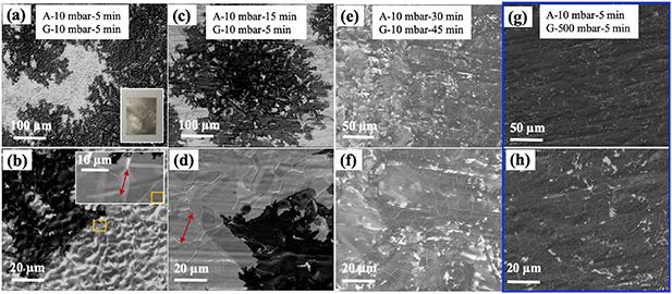
Figure 1. SEM images of NGF growth at 900 ºC and various pre-annealing and growth conditions for samples NiAG1- 4 (refer table 1). (a), (c), (e), (g) low-magnification SEM images (in the inset of each panel—A = annealing parameters and G = growth parameters) and corresponding high-magnification images are presented in (b), (d), (f), (h), respectively. SEM images of the optimized sample (NiAG4 sample) are marked with blue outline. A digital photo of a typical sample (3.5 × 2.5 cm2) with non-uniform NGF growth is shown in the inset of panel (a). Two typical Ni grains are marked with red arrows in panel (b) inset and panel (d). Also, refer to figure SI2 for additional results.
Download figure:
Standard image High-resolution imageTable 1. A list of samples and their short names with varied process parameters to obtain NGF growth. Other process parameters such as same temperature during annealing and growth, chamber pressure during annealing (10 mbar) were kept constant. Pre-annealing time = At, chamber pressure during growth = Pg, growth time = Gt. Here, only selected experiments are given to show the NGF growth optimization process. For instance, NGF growth with the same parameters as NiAG7 but Gt = 5 min growth step or Pg = 10 mbar were not added here, as they result in non-uniform growth, similar to NiAG1.
| Processing | T (°C) | At (min) | Pg (mbar) | Gt (min) | Short-name |
|---|---|---|---|---|---|
| None, as-received Ni foil | – | – | – | – | NiAR |
| Annealed | – | 5 | – | – | NiA |
| Ni foils annealing and NGF growth | 900 | 5 | 10 | 5 | NiAG1 |
| 15 | 10 | 5 | NiAG2 | ||
| 30 | 10 | 45 | NiAG3 | ||
| 5 | 500 | 5 | NiAG4 | ||
| 30 | 500 | 5 | NiAG5 | ||
| 5 | 500 | 2 | NiAG6 | ||
| 700 | 5 | 500 | 45 | NiAG7 |
We further evaluated the extent of growth uniformity in the NiAG4 sample in a typical photo of the NGF/Ni sample, as shown in figure 2(a). Unlike the as-received Ni foil, the color of the treated sample changed from shiny metallic gray to dull gray, all over the 50 cm2 sample (unlike for the NiAG1 sample, figure 1(a), inset). This visual change indicates a wafer-scale uniform growth over large-area. After its reproducibility was confirmed, the process parameters for the NiAG4 sample were identified as the optimal conditions for NGF growth.

Figure 2. (a) Photo of typical NGF sample (NiAG4) showing uniform wafer-scale NGF growth (50 cm2). (b)–(d) Raman spectroscopy results of NGF/Ni grown at optimized conditions: (b) optical microscopy image of the mapped area marked by a mapping grid. (c) Raman mapping result (8 x 37.5 µm2, 0.5 µm step)—I2D/IG ratio, (d) normalized Raman spectra (to have identical G peak intensity) at different positions with representative color in the map of panel (c), TLG = Tri-layer graphene.
Download figure:
Standard image High-resolution imageWe cut the NiAG4 sample into pieces and inspected further to obtain detailed information on the quality of the as-produced NGFs. The high-magnification images were not recorded from the same regions as that of the corresponding low-magnification to avoid analyzing areas which were contaminated with the aggregation of secondary electrons from the electron beam (figure SI3). The bright areas coverage estimated from SEM images (an example shown in figures SI4(a) and (b)) was 0.1%–3% in 100 µm2. Although the relative percentage of bright areas is significantly lower, hereafter, for further characterizations, we have chosen areas consisting of both bright and dark areas, irrespective of their actual relative area coverage. The light and dark contrast observed here is a simple and qualitative measure to recognize the presence of FLG and MLG areas in the NGF film and not a quantitative assessment for how many numbers of graphene layers are present. For quantitative analysis, regarding NGF thickness, we used additional techniques such as Raman, TEM and, AFM, as discussed below. The stepped Ni texture shown in the AFM image (figures SI5(b) and (c), marked with red arrow) can be associated with bright areas of SEM images (figure SI5(a)). The root mean square (RMS) roughness of 40 nm was found from the AFM image in figure SI5(b) (10 x 10 µm2). The fold defect density on the NGF surface was 20–70 folds/100 µm2, as estimated from the SEM and AFM images (figures SI4(c) and (d)).
By using optical microscopy (NiAG4 sample), we observed the dominant presence of dark regions (figure 2(b)). A Raman map was performed to include both dark and bright regions marked with an overlapping grid in figure 2(b). A typical spectrum consists of the characteristic graphite peaks, such as G (E2g mode, at 1580 cm−1), D (defect-activated breathing mode at 1350 cm−1), and 2D (overtone at 2750 cm−1) [36]. The presence of G and 2D peaks pointed to a highly crystalline graphitic material. D peaks with small intensity were observed rarely and only in the few-layer graphene regions. Figure 2(c) presents the intensity ratio map of the 2D and G peaks (I2D/IG) [36]. The I2D/IG values correlate well with the number of graphene layers [18, 37]. Normalized Raman spectra (with respect to G peak intensity), taken at different positions and representative of the colors in the map, are shown in figure 2(d). Clearly, the I2D/IG values vary depending upon the probe position. The red area in figure 2(c) (corresponding to the bright region in figure2(b)) relates to bilayer- and trilayer-graphene (I2D/IG ratio of ∼1.1 and 0.9, respectively) [18, 37]. On the other hand, the blue area in figure 2(c) (corresponding to the dark regions, figure 2(b)) shows I2D/IG ratios of ∼0.3. These ratios are similar to graphite; thus, the NGF in these regions must be composed of four or more graphene layers. In addition, the commonly observed broadening and upshift of the 2D peak (related to the increasing number of graphene layers) are shown in figure 2(d). Finally, the G peak position is almost constant in all spectra, indicating the absence of chemical doping in the graphene layers.
The crystalline quality of the Ni foils before and after NGF growth was analyzed by XRD. The XRD patterns for the NiAR and NiA samples (table 1) are displayed in figure 3(a). In the NiAR, peaks at 2θ = 44.4º and 51.7º were observed. The 2θ values are in good agreement with the standard values of the (1 1 1) and (2 0 0) Ni crystal planes [38]. In the NiA, the (1 1 1) peak intensity increased by 1.5 times in relation to the (2 0 0). This higher intensity indicates a preferential (1 1 1) orientation of the grains in the annealed Ni foil. Also, as shown in figure SI6 (SEM image and EBSD mapping of the sample surface), Ni surface grains with mainly (1 1 1) orientation resulted from the recrystallization process during annealing [30, 34, 39]. In the NGF-growth samples (NiAG2 and NiAG4), an additional peak in the XRD pattern was observed at 2θ = 25.6º (figure 2(b)). This 2θ value corresponds to the 0.335 nm interplanar distance of (0 0 0 2) graphite planes [28, 40]. A relatively lower (0 0 0 2) peak intensity was observed for the 15 min pre-annealed Ni sample than the 5 min one, which correlates well with the formation of the thinner and non-uniform NGF on the NiAG2 sample (figure 1). Longer annealing offers large Ni (111) grain formation, which is favorable for FLG growth [30, 41]. However, not all grains have (111) surface orientation. Smaller grains with different orientation and grain boundaries will contribute to MLG growth, which leads to non-uniform NGF growth at low Pg during growth [18, 30].
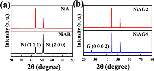
Figure 3. XRD results: (a) for as-received Ni foil and 5 min annealed Ni foil, (b) for NGF grown at two different pre-annealing times.
Download figure:
Standard image High-resolution imageThe as-grown film was transferred on a SiO2/Si substrate (digital photo of a typical sample shown in figure 4(a)) by an improved wet chemical transfer process [30, 34]. A uniform film with dark grey color can be seen with the naked eye. Typical SEM images (figures 4(b) and (c)) for the same sample confirm continuous large-area NGF growth (major dark areas). Further studies on the as-grown and transferred film properties such as conductivity and transparency is reported elsewhere [42].

Figure 4. (a) Typical digital photo of the transferred NGF sample (NiAG4) using improved wet chemical transfer technique on SiO2/Si, with the NGF film enclosed in a dotted orange square. (b) and (c) Typical SEM images of the same sample. The red, blue, and yellow arrow indicate dark and bright areas, and fold, respectively.
Download figure:
Standard image High-resolution imageResearchers have attempted to control the graphene/ultra-thin graphite films by tuning process parameters such as growth temperature, hydrocarbon exposure (limiting the amount of C by maintaining ultra-high vacuum conditions), substrate thickness (precipitation control), and post-cooling rates (fast cooling, slow precipitation) [41, 43]. The solubility and diffusivity of C in Ni at 900 °C are 0.8 at. % and 8.5 × 10⁻⁸ cm2s–2, respectively [27]. At higher temperatures, these values are higher [27, 28]. After the growth step, when the Ni catalyst is cooled below 900 °C, the C precipitates at the surface of the Ni as a graphite thin film [43]. However, the rates of C precipitation differ for differently oriented grains and at the grain boundaries, so achieving uniformity in thickness over large-area polycrystalline Ni substrate has remained challenging [41, 44]. We obtained extended NGFs by tuning the At and Pg. Extended At favors larger Ni (1 1 1) grain formation (figures 1(b) and (d)) whereas short At results in a fewer Ni (1 1 1) grains with smaller sizes (figure SI6, 1–10 µm). Ultrathin graphite film formation is favored on Ni (1 1 1) [44, 45]. In our case, short At time might be responsible for dominant NGF growth with low FLG coverage (0.1%–3% areas in 100 µm2). Another critical process parameter is Pg. When Pg was higher (500 mbar), more C was dissolved in the Ni foil, and it resulted in relatively more uniform NGF upon cooling than those grown at 10 mbar. Thus, we were able to produce the NGFs with uniformity at mm2-scale when the two key process parameters At and Pg were controlled.
3.2. Structural analysis of NGF/Ni
As discussed above, we attribute the contrast in SEM images to variations in the thickness of NGF. Figure 5(a) shows a thicker sector of the NGF that was characterized by a black contrast in the SEM secondary-electron imaging (figures SI7(a) and (b)). The TEM observation revealed a highly oriented, defect-free state of the graphene layers, also confirmed by the fast Fourier transform (FFT) pattern (figure 5(a), inset). The graphene layers have a typical (0 0 0 2) lattice-spacing of 0.33 ± 0.01 nm in this section, and the NGF thickness is about 100 nm, with a flat surface. And moving laterally along the NGF, we found two characteristic structural faults. In the first case, due to tangential stress along the graphite film, the NGF forms rippled textures associated with local delamination of the graphitic layers (figure 5(b)). This phenomenon, named as ripplocation, is well known and documented in those layered crystalline materials where the combination of the tangential stress and the strain perpendicular to the layer can generate folded structures without brittle damage [46–48]. In the second case, in those areas of the Ni substrate characterized by a gentle zig-zag topography of a few tens of nanometers, the graphene layers arrange by following the concave and convex interface (figure SI8(c)). As a result, they form symmetrical chevron-like nano-folds with dislocation fields along the fold axis (figure 5(c)). Differently from these, when the Ni substrate shows extended zig-zag surfaces of hundreds of nanometers (steps with small slope, figure SI8(d)), the NGF cannot arrange by a perfect folding, but it gives rise to the formation of kinked structures characterized by brittle damage and very sharp dislocation fields separating the NGF blocks with different orientation. In particular, the graphitic structure in the core region of these kink bands shows large delamination and the gaps filled by amorphous carbon (figures 5(d) and (e)). The HRTEM image of the gap region at the interface NGF/Ni is shown in figure 5(e). The graphene layers exhibit a lattice spacing slightly expanded, 0.35 ± 0.01 nm (instead of 0.33 ± 0.01 nm), compatible with the formation of a mixed NiCx phase [41]. The FFT pattern of the Ni substrate (figure 5(f)) is consistent with the Ni [−1 1 2] zone axis projection, displaying how the Ni (1 1 1) surfaces are exposed to the NGF. We observed that the secondary phases of NiCx were not formed continuously along the Ni substrate. Where present, they displayed an arrangement of the basal lattice planes parallel to those of the Ni (1 1 1), resulting in an epitaxial symmetry relationship with the substrate. Figures 5(g) and (h) show a different region of the host Ni substrate where the NiCx phase interposes between the NGF and Ni substrate, preserving the same orientation of the Ni (1 1 1) lattice planes. The restructuring of NGF into ripplocation, nanofolds and kinks can occur during the cooling process as there is a significant difference in thermal expansion coefficients between Ni and graphite [49, 50].
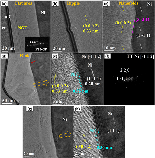
Figure 5. Cross-section TEM observations of the dark regions of NGF (NiAG4): (a) Image in flat area with FFT pattern in the inset, (b) Image of a ripple on NGF surface; yellow line indicates graphite crystal plane, (c) Twins in NGF originating from Ni grain with zig-zag steps, pink and white lines indicate Ni crystal planes, (d) NGF with kink formation on a Ni grain with a small slope step (marked with a red arrow). (e) High-resolution image near the Ni grain step in panel (d), (f) FFT pattern for Ni substrate. (g) and (h) Another region showing the presence of NiCx at the NGF/Ni interface.
Download figure:
Standard image High-resolution imageIn addition to the dark contrast regions, a thinner sector of the NGF (characterized by a bright contrast in SEM secondary-electron imaging, refer to figures SI7(a) and (c)) was also analyzed. Figure 6 displays the corresponding cross-section TEM analysis. The continuous NGF at the nanometer scale is shown in figures 6(a) and (b): a gentle folding texture in the NGF that links areas with few hundreds of graphene layers and few tens of graphene layers. Such links were observed in the areas where the Ni substrate has steps of large slopes (figure SI8(e)). For example, as shown in figures 6(c)–(g), FLG is in contact with Ni grains (∼1–10 µm, figures SI8(a) and (b)) with nanoscale surface steps. These grains could be correlated to the large (111) grains observed in NiA sample (figure SI6), which further undergo size reduction and recrystallization during the growth step; similar grain transformation were observed previously [20]. HRTEM imaging of the bi-layer graphene (BLG) regions (figures 6(d) and (e)) reveals a perfect and continuous crystal structure showing the typical graphite (0 0 0 2) lattice spacing of 0.33 ± 0.01 nm. In certain regions, at the interface of FLG/Ni (figures 6(d) and (e)), two layers characterized by a lattice spacing of 0.35 ± 0.01 nm were observed. We attribute this extended spacing to the presence of a mixed NiCx phase, as in the case of a thicker NGF sector (figure 5(e)). Here, for proper alignment of the FLG/Ni interface for HRTEM imaging, the Ni crystallite of this sector was oriented along the [–1 1 0] zone axis with the Ni (1 1 1) surface parallel to the electron beam. The HRTEM that measured a graphitic (0 0 0 2) lattice spacing of 0.33 ± 0.01 nm for the BLG is shown in figures 6(f) and (g). Here the Ni crystal was aligned along the [2–2–1] zone axis to expose the Ni (1 1 1) surface correctly for the imaging. Overall and thanks to a cryo-FIB preparation associated with a gentler ion beam setting, not only could we able to preserve the structure of the FLG sectors, including areas with BLG, but we could also image these layers successfully.
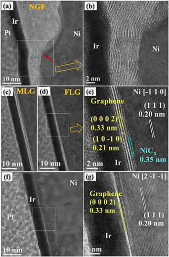
Figure 6. Cross-section TEM observation of the NGF in the bright regions (NiAG4): (a) Low-magnifications image showing the connection between NGF and few-layered graphene areas with a large slope step (marked by an red arrow). (b) High-resolution image for the area marked with white square in panel-a. (c), (d), (f) NGF films in different areas showing the presence of MLG, FLG and, SLG regions, respectively. (e) and (g) High-resolution images for the area marked with white squares in panel-d and panel-f, respectively.
Download figure:
Standard image High-resolution imageInterestingly, in some of the FLG sectors, we found that an atomic interface mediates the contact between the FLG layers and the Ni substrate via an epitaxial relationship, as shown in figures 7(a) and (b). In particular, this sharp interface layer of C atoms follows the flat Ni substrate facet (1–1 1) perfectly. In this HRTEM image, we can see its basal and perpendicular lattice planes with 0.17 ± 0.01 nm and 0.21 ± 0.01 nm, respectively. The distance between the interface and the topmost Ni layer was found to be 0.19 ± 0.01 nm. This distance matches with the distance between graphene and the topmost layer of Ni(111) measured by low energy electron diffraction pattern analysis (0.21 ± 0.007 nm) [51] and theoretical calculations (0.205 nm) [52]. These values indicate that the interface layer is nothing but a tightly bonded graphene with a Ni substrate (in this region).

Figure 7. Cross-section TEM study of the NGF in the bright regions (NiAG4): (a) TEM image showing the presence of a sharp interface between the FLG and Ni substrate, (b) High-resolution image for the area marked with white square in panel (a). (c) Schematic showing the epitaxial relationship between few-layered graphene and Ni (111), mediated by a monolayer of C atoms. Dark green and purple spheres represent C atoms from the backside plane
Download figure:
Standard image High-resolution imageThe FLG layers growing on such interface are homogeneous, with a slightly wavy profile ascribable to the tangential stress. After the growth step, as the temperature decreases lower than 900 ºC, the C solubility in Ni decreases, the carbon atoms are expelled to the surface and form a separated phase [43]. The occurrence of the interface layer suggests that an atomic C layer grows on the flat Ni (111) substrate by C precipitation. In parallel, spontaneously expelled C atoms from the Ni grain boundaries form the additional FLG layers [45, 53]. These TEM observations (of the presence of NGF and FLG regions) agree with the SEM and Raman results (figures 1 and 2).
During the growth process, the C atoms are produced by pyrolytic reactions between H2 and CH4 . These C atoms dissolve into Ni substrate at elevated temperatures (the C diffusivity/solubility in Ni is temperature-dependent). Studies report that the NGF growth can occur by preferential carbon precipitation in C-enriched Ni films [18, 41] and nucleation of graphite/graphene layers on the metal substrate surface upon sample cooling steps. Studies also reported an epitaxial growth of structurally homogeneous graphene (0 0 0 2) with excellent physical properties on the lattices of Ni (1 1 1) [43]. The lattice mismatch ( can be defined as the absolute difference between two lattice spacings (
 ) along a certain crystal direction, relative to the average of the lattice spacings [54]:
For example, in the case of FLG (figures 6(d), (e), and 7), we can identify the following epitaxial relationship:
- (a)Ni (1 1 1)//FLG (0 0 0 2)
- (b)Ni [–1 1 0]//FLG [1 0 –1 0]
- (c)Ni [1 1 –2]//FLG [0 1 –1 0],
where the first term represents the planar alignment and the other two vector alignments, respectively. The corresponding calculated  values are 49%, 19%, and 39%, respectively. These results are consistent with a semi-coherent NGF/Ni interface along which: (a) three Ni [11 1] lattice units fit two FLG [0 0 0 2] lattice units, (b) five Ni [–1 1 0] lattice units fit six FLG [1 0 –1 0] lattice units, and (c) three Ni [1 1 –2] lattice units fit four FLG [0 1 –1 0] lattice units. This epitaxial relationship is consistent with the literature data that indicates the Ni (1 1 1) surface as a preferable nucleation and growth site for graphene, with the value graphene/Ni adhesion energy being 72.70 Jm−2 [55, 56].
The plan-view TEM imaging for the transferred NiAG4 sample on Cu grid (with lacey C film), presented in figure SI9, shows the presence of the FLG, MLG sections. Unlike SLG [18], we were successful in achieving cracks- and contaminant-free transfer of NGFs which contained FLG areas (few microns wide) partially suspended TEM grid with lacey carbon (figure SI9(a)). These FLG sections were found to be intact and well connected to the NGF. SAED patterns were acquired at 19 different spots to assess the structural features of the NGFs. The grain size of the NGFs varied in the range of a few μm2 to tens of μm2. In the FLG section, the SAED pattern was consistent with two sets of FLG {0 0 0 1} sheets characterized by a rotational mismatch of 20°, and thus giving rise to (1 0 –1 0) and (1 1 –2 0) spots with a very weak intensity (figure SI9(c)). In this sector, we could discriminate thinner FLG generating weak diffraction spots arranged circularly. But in the NGF section (figure SI9(f)), the SAED pattern was consistent with polycrystalline diffraction spots arranged circularly and showed different intensities. This presence of several spots is the typical effect of random rotational mismatched layers generating a kind of polycrystalline diffraction pattern (figures SI9(c)–(f)).
Generally, graphite films grown on Ni substrate have folds on the surface [23, 26]. These folds arise because the thermal expansion coefficients of Ni (4.7 to 7.7 × 10⁴/°C [49]) and graphite (0.4 to 1.3 × 10⁻⁶/°C [50]) are different (for the temperature range 300 °C–1000 °C). Researchers have assumed that the compressive stress is developed between the Ni substrate and graphite film during the cooling step, and that is what gives rise to the formation of folds on graphene/graphite films [26, 32]. It has been also speculated that the surface steps could be responsible for fold formation [57]. Our results, obtained from SEM, AFM, Raman and TEM, reported in the results section confirm that a close connection exists among the number of graphene layers in NGFs, surface defects, and morphology of the substrate topography of Ni. Our cross-section TEM images evidence that Ni surface steps have a significant role in the fold formation (figures 5 and 6), which is demonstrated in a model shown in figure 8. More details regarding the various NGF/Ni samples (SEM and TEM) are provided in figure SI8. The model shows a continuous NGF and not a single continuous graphene layer on the top. Some graphene layers with exposed edges (especially in FLG areas) might exist on the NGF surface, as observed in figure 7. In the model, we show the compressed strain induced kink formation close to the large Ni grains with small slope. Also illustrated, nanofolds occurred at zig-zag steps of Ni surfaces while the ripples are not associated with surface steps.

Figure 8. Model for NGF growth with respect to Ni surface topography (also refer figure to SI8). The white lines indicate graphene layers of NGF in cross-section view. The blue planar sheets indicate graphene layers of NGF. The number of graphene layers in the schematic is merely illustrative.
Download figure:
Standard image High-resolution image
We believe that our method (with a 5 min growth step) could be applied to obtain continuous NGFs in higher throughput and at lower temperatures (900 ºC) than those of the recently proposed graphite film growth methods [15, 23, 58]. These reported other methods require complicated steps, longer process times and temperatures in the range 1000 ºC –3200 ºC. Finally our TEM observations revealed the following: (i) epitaxial growth of NGF on Ni (111) grains and (ii) the crucial role the polycrystalline nature and topography of the Ni foil in the formation of the NGF texture and the number of graphene layers. Our findings would be a guiding step to obtain the NGFs free of folds by precisely tuning the Ni grain-size and performing surface topography engineering.
4. Conclusions
We developed a fast wafer-scale CVD method to grow high-quality NGFs (∼100 nm) with mm2-scale uniformity. By contrast to analogous approaches, our 5 min growth-step significantly reduces the time and cost to produce these large-area graphitic films on polycrystalline Ni foils. Cross-section and plan-view electron microscopy identified µm-scaled FLG regions and we analyzed them in detail. Besides our unprecedented imaging of the interfaces, structural defects (ripples, kinks, nanofolds) and rotational stacking faults, we also studied the thickness variations of the graphite films and related them to the substrate's grains and surface topography through a simple model. Hence, the as-grown NGFs are <300 graphene layers thick but have interlinked sections with < 30 layers (0.1%–3% areas in 100 µm2). Interestingly, the presence of these FLG sections does not compromise the mechanical integrity of the cm2-films because they could be transferred without tearing (via a conventional wet chemical transfer method), to rigid substrates and TEM grids.
In the future, we envisage that the production of the fast-grown NGFs on Ni can be scaled up by means of a roll-to-roll CVD method, akin to what has been developed for graphene on Cu foils, for their use in technological applications such as electronic circuits heat-sinks or fire retardant barriers.
Acknowledgment
This work was supported by KAUST (BAS/1/1346‐01‐01). We thank Xavier Pita (a scientific illustrator at KAUST) for preparing Figures 8 and Lina Mynar for technical english corrections of the manuscript.