

Abstract
The terahertz (THz) frequency range is very important in various practical applications, such as terahertz imaging, chemical sensing, biological sensing, high-speed telecommunications, security, and medical applications. Based on the density functional theory (DFT), this work presents electronic and optical properties of N-doped ZnO/ZnO/N-doped ZnO quantum well and quantum wire nanostructures. The density of states (DOS), the band structures, effective masses, and the band offsets of ZnO and N-doped ZnO were calculated as the input parameters for the subsequent modeling of the ZnO/N-doped ZnO heterojunctions. The results show that the energy gaps of the component materials are different, and the conduction and valence band offsets at the ZnO/N-doped ZnO heterojunction give type-II alignment. Furthermore, the optical characteristics of N-doped ZnO/ZnO/N-doped ZnO quantum well were studied by calculating the absorption coefficient from transitions between the confined states in the conduction band under the applied electric field (Stark effect). The results indicate that N-doped ZnO/ZnO/N-doped ZnO quantum wells, quantum wires, and quantum cascade structures could offer the absorption spectrum tunable in the THz range by varying the electric field and the quantum system size. Therefore, our work indicates the possibility of using ZnO as a promising candidate for infrared and terahertz applications.
Export citation and abstract BibTeX RIS
1. Introduction
Terahertz radiation (THz) refers to a broad electromagnetic spectrum range between microwaves and infrared waves (0.1 to 10 THz), also known as the terahertz gap. This spectral range provides a variety of possible applications including imaging, chemical sensing, biological sensing, high-speed telecommunications, security, optoelectronics, and medicine [1–10]. However, one of the major challenges in THz technology is the difficulty in finding suitable materials capable of providing energy efficient THz sources, because metals are typically not suitable due to the absorption losses at these frequencies [11]. With the rapid development in fabricating advanced nanomaterials in the past decades, the THz research field has significantly expanded. Novel semiconductor nanostructures such as quantum wells, quantum wires, quantum dots, and quantum cascade structures, were demonstrated as high-power sources of THz [12], using the quantum confinement and intersubband (intraband) transitions. In particular, group III–V semiconductor heterostructures have received much attention [12]. Furthermore, there has been an increasing interest in alternative materials, such as transparent conducting oxides (TMOs), e.g. ZnO, TiO2, SrTiO3 [10, 13–18].
Among TMOs, nanoengineered ZnO-based semiconductors, which are biocompatible materials, have attracted a lot of research attention in the THz area, because they are promising materials for THz sources at the room temperature, with potential for high output power. It can also be used for THz detectors with higher operating temperatures than possible with the current AlGaAs/GaAs system. These devices are usually based on the multiple quantum well and quantum cascade concept and take advantage of the unique properties of ZnO, i.e. good electrical transport, high electron mobility, higher value of longitudinal optical (LO) phonon energy, higher conduction band offset (CBO), excellent optical properties in a wide THz range [10], band gap engineering via doping [19–21], and availability of various nanostructures, including nanowires and nanoparticles [19, 20, 22–26]. Moreover, N-doped ZnO thin films have been successfully grown by various techniques, such as molecular beam epitaxy, pulsed laser deposition, ion beam sputtering, ion implantation and magnetron sputtering. In particular, our previous work has revealed that the band gap of ZnO can be reduced by doping with nitrogen [21]. Hence, one can fabricate ZnO/N-doped ZnO heterostructures to create quantum confined systems in order to achieve intersubband (intraband) transitions in the THz range. In case of simplicity, periodic MQW structures, the operation as THz detectors should be straightforward and does not require extremely precise growth. THz emitters like quantum cascade lasers usually require more complicated layer sequence with quite precise growth and this would be second stage of development. In this work, we study the electronic and optical properties (absorption spectrum) of ZnO/N-doped ZnO in the infrared and terahertz frequency range. Based on the density functional theory (DFT), we have found that ZnO/N-doped ZnO heterostructure exhibits type-II band offset. The external electric field applied to quantum confined structures can engineer their absorption spectrum to be in the THz range, by varying the field magnitude and the size of the quantum well.
2. Computational details
The first principles DFT calculations using Perdew-Wang-Earnzehof (PBE) formalism were employed to optimize 2 × 2 × 2 supercell of N-doped ZnO structures, containing 32 atoms. After that, the optimized structures, DOS and band structure were calculated using hybrid Heyd-Scuseria-Ernzehof (HSE) [27] functional with the Hartree–Fock exchange mixing parameter of 37%. This mixing ratio is the value necessary to reproduce the experimental gap of ZnO. Additionally, 7 × 7 × 5 k-point grid in the Brillouin zone and the plane wave cutoff energy of 400 eV were employed, while Zn(3d104p2), O(2s22p4) and N(2s22p3) electrons were treated as valence electrons. As for the doping, one O site in the supercell was replaced by a N atom, hence the nitrogen doping percentage is 6.25 mole percent. The band alignment of the heterojunction was calculated from the work functions, and the offset magnitudes were subsequently used to create the potential wells in the confined quantum well systems using the effective masses of holes and electrons of ZnO and N-doped ZnO. The eigenstates of carriers confined in the quantum wells with or without the external electric field were calculated by the effective-mass finite-difference approach. These solutions were further used to calculate the dipole moment and the adsorption coefficient.
3. Results and discussion
The calculated lattice parameters and optimized structures are shown in table 1 and figures 1(a), (b), respectively. Considering the lattice parameter, c/a ratio of N-doped ZnO is larger than that of the undoped ZnO, due to a larger atomic radius of nitrogen.
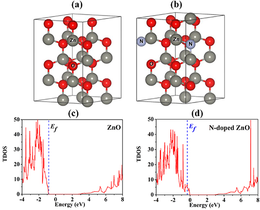
Figure 1. Optimized structures of (a) ZnO and (b) N-doped ZnO, with grey spheres representing the zinc atoms, red the oxygen, and blue the nitrogen, and TDOS of (c) ZnO and (d) N-doped ZnO super-cells.
Download figure:
Standard image High-resolution imageTable 1. Optimized lattice parameters of ZnO and N-doped ZnO.
| Structures | Lattice parameters | |||
|---|---|---|---|---|
| a (Å) | c (Å) | alpha (˚) | gamma (˚) | |
| ZnO | 6.52 | 10.52 | 90.00 | 120.00 |
| N-doped ZnO | 6.50 | 10.54 | 90.00 | 120.00 |
The next step is the calculation of the total density of states (TDOS) of ZnO and N-doped ZnO using the hybrid functional from the HSE approach. Figures 1(c), (d) show the TDOS of the studied structures. The DOSs changes when the N atom is doped into ZnO. This result is in accordance with the DFT calculation, as we have previously reported [21]. The partial DOS and projected DOS, as illustrated in figures 2–3, show that the valence band maximum is predominantly formed by electrons in d-orbital of Zn, p-orbital of O and p-orbital of N. The comparison of DOS between undoped ZnO and N-doped ZnO shows that the replacement of an O atom by N causes the change in DOS of the host structure. Nitrogen interacts with Zn and O, resulting in the creation of new states, especially at the top of the valence band. In other words, adding nitrogen can increase the density of electrons at the top of the valence band. Based on that, one can expect that the larger density of electrons near the valence band maximum of N-doped ZnO can provide beneficial optical properties and enable it to reach high photocatalytic performance under visible range radiation.

Figure 2. Partial and projected DOS (PDOS) of the 2 × 2 × 2 pure ZnO supercell: (a) partial DOS of Zn, (b) projected DOS of ZnO, (c) partial DOS of O, (d) projected DOS of O.
Download figure:
Standard image High-resolution image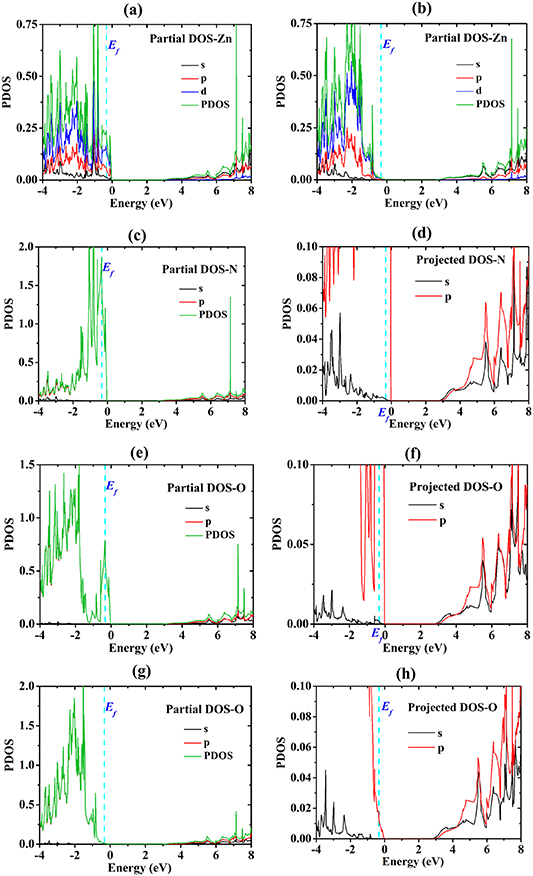
Figure 3. Partial and projected DOS (PDOS) of the 2 × 2 × 2 N-doped ZnO supercell (a) partial DOS of Zn, (b) projected DOS of Zn, (c) partial DOS of O, (d) projected DOS of O (e) partial DOS of N, (f) projected DOS of N.
Download figure:
Standard image High-resolution imageAfter that, the band structures of ZnO and N-doped ZnO are calculated using the HSE and shown in figure 4. Both ZnO and N-doped ZnO systems are direct bandgap semiconductors with e.g. of 3.31 and 3.03 eV respectively, in accordance with experimental reports [19, 20, 28–30]. It is clear that the N doping reduces the bandgap of ZnO, according to the DOS results. Thus, this work considers the possibility of using the difference of band gaps of ZnO and N-doped ZnO in order to design a quantum well based on the ZnO/N-doped ZnO heterojunction.

Figure 4. Corrected band structures of (a) ZnO and (b) N-doped ZnO.
Download figure:
Standard image High-resolution imageTo study the depth of the quantum well in this system, the potential energy at any position in ZnO and N-doped ZnO materials is calculated and shown in figure 5(a). Then, the average potential V, defined as the difference of maximum and minimum values divided by two, is set to zero. This energy is the potential reference for both ZnO and N-doped ZnO in this study. As for the positions of ZnO and N-doped ZnO atomic arrays on the z-axis, ZnO extends from 0.00 to 10.51 Å and then, for z > 10.51 Å it is N-doped ZnO. From the graph, the potential difference between ZnO and N-doped ZnO is 0.23 eV. Therefore, such a quantum well can efficiently confine carriers, because the height of the barrier is larger than the room temperature thermal energy ET, which is about 0.03 eV (ET = kBT, where kB and T are the Boltzman constant and temperature, respectively).

Figure 5. (a) In-plane average potential plot of ZnO and N-doped ZnO, (b) band alignment in ZnO/N-doped ZnO junction, and (c) ZnO/N-doped ZnO heterostructure designed as a quantum well, not to scale, where grey and yellow areas are ZnO and N-doped ZnO, respectively.
Download figure:
Standard image High-resolution imageThe band alignment in the ZnO/N-doped ZnO heterojunction is shown in figure 5(b). The values of CBO and valence band offset (VBO) in this system are 0.39 and 0.67 eV, respectively. Additionally, the conduction band bottom of this well is in ZnO, while the valence band top is in N-doped ZnO. This indicates that the system is a type II-staggered heterojunction, with 2.64 eV band edge (or e.g.) offset, calculated as CBMZnO-VBMN-doped ZnO. This band alignment is in qualitative agreement with the report of Qin et al [31]. However, the band offset values on the real scale were not reported in that paper, while the real scale and other details of this heterojunction are reported in this work.
In the next step, the quantum well based on ZnO/N-doped ZnO heterojunction is modelled using the obtained band alignment as shown in Figure 5(c). From the obtained results, this heterojunction can be expected to be a promising quantum well photocatalyst, because the band-gap offset corresponds to the solar radiation spectrum. Electrons can hop from the valence band of N-doped ZnO into the conduction band of ZnO by absorbing photons with energy equal to or larger than 2.64 eV, corresponding to 469.64 nm (visible range). Electrons can then freely move in the conduction band of ZnO, while holes remain in N-doped ZnO. On the other hand, holes in the valence band of ZnO can move into higher energy states (on the absolute scale) in the valence band of N-doped ZnO. This prolongs the electron-hole recombination time, leading to increased photocatalytic reaction rates.
The next question is about the properties of carriers confined in this quantum well. This requires the effective masses of the particles to be extracted, and table 2 contains the effective masses in ZnO and N-doped ZnO, calculated as  , where m* is the effective mass for the particular band, ħ the Planck's constant divided by 2π, and
  the energy dispersion of that band, obtained by fitting the parabola to the calculated band dispersion. Only the effective mass in the direction perpendicular to the c-axis, from the center of the Brillouin zone (Γ point) to M symmetry point, is studied. The reason for choosing this path is because it shows a larger change in energy, while the band is quite flat in the parallel direction (Γ-A), as seen in figure 4. The calculated effective masses of electrons and light holes in ZnO are quite close to experimental values, 0.29m0 and 0.59m0, respectively [32, 33]. Comparing the effective masses of carriers in ZnO to those in N-doped ZnO, the effective masses of electrons in N-doped ZnO are smaller than in ZnO. This is clear from the larger curvature of band structure around CBM in N-doped ZnO than in undoped ZnO.
Table 2. Effective masses of carriers in ZnO and N-doped ZnO structures in Γ-M direction, where me, mlh and mhh are the effective mass of electrons, light holes, heavy holes, and m0 is the free electron mass.
| Carriers | ZnO | N-ZnO |
|---|---|---|
| me | 0.2724m0 | 0.2694 m0 |
| mlh | 0.3115 m0 | 0.2683 m0 |
| mhh | 1.5431 m0 | 0.3884 m0 |
4. Heterostructures
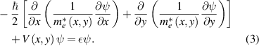
In this work, the quantum well and quantum wire nanostructures based on N-doped ZnO/ZnO/N-doped ZnO (denoted as NZnO/ZnO/NZnO) are considered. The microscopic view of the structures are as shown in figure 6, but the effective mass method (single band method, within the envelope function approximation) is employed to solve the envelope function Schrodinger equation. From the previously calculated results, the conduction band discontinuity between NZnO/ZnO/NZnO is taken as 0.39 eV and the effective masses of ZnO and N-doped ZnO are 0.2694 m0 and 0.2724 m0, respectively. In order to include the effect of position-dependent effective mass,  , the one-dimensional Schrodinger equation for the quantum well is

Figure 6. Microscopic view of N-doped ZnO/ZnO/N-doped ZnO heterostructure designed as (a) a quantum well and (b) a quantum wire, where yellow represents N-doped ZnO and pink represents ZnO.
Download figure:
Standard image High-resolution imageThis is written in the finite difference form as
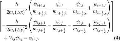
For the NZnO/ZnO/NZnO quantum wires, the two-dimensional Schrodinger equation with the position-dependent effective mass,  , is
, is
and in the finite difference form, this is written as
To consider the Stark effect in quantum wells and quantum wires with the applied electric field, the effective mass method was also employed. The Schrodinger equations for the quantum well and wire take the following forms,
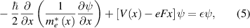
and

for the quantum well and the quantum wire, respectively. The electric field (F) was set in the x-direction and the reference zero of the electrostatic potential is in the center of the quantum well or the quantum wire, being convenient for the comparison of quantized state energies variation with the applied electric field. The finite-difference forms of these equations now become
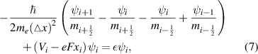
and,

After finding the quantized states of nanostructures, their optical properties were calculated, by finding the transition dipole moment between the ground state and other excited confined states. The absorption coefficient coming from electron transitions between the ground state and other states is

where  is the photon frequency,
  the refractive index,
  the velocity of light,
  the line profile,
  the intersubband dipole moment,
  the nanostructure volume,
  the permittivity of the nanostructure. In addition,
  and
and  are the carrier populations of the ground state and the other confined state, respectively. For the line profile, a simple normalized Lorentzian form was used
where  is the half-width (Lorentzian broadening) coming from dephasing effects, and in this calculation, it was taken as 0.005 eV. Furthermore, the dipole moment is calculated with normalized envelope wavefunctions (along the quantum well growth direction x) as
where e is the electron charge. Therefore, the absorption coefficient depends on  . The calculated results for these heterostructures are shown in figures 7–9. They show the energy states and wave functions in quantum wells and quantum wires based on N-doped ZnO/ZnO/N-doped ZnO heterojunction. State energies, depending on the quantum well width, are given in figure 7. Increasing the quantum well width from 4 to 10 nm results in lower state energies: E2-E1 is about 0.14 eV for 4 nm quantum well and 0.03 eV for 10 nm quantum well.
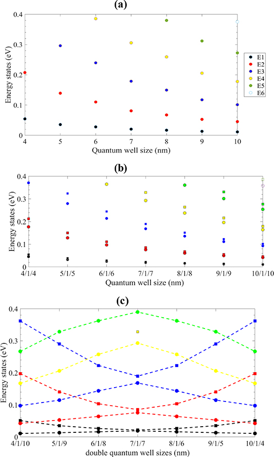
Figure 7. State energies vs. quantum well size dependence for (a) quantum well, (b) double quantum well, and (c) asymmetric double quantum well.
Download figure:
Standard image High-resolution imageFigure 8(a) shows the wave function in the quantum well. The wave function moves to the right when 80 kV cm−1 electric field is applied and its ground state energy decreases slightly, in the same direction as for 2nd state and 3rd state. The reason is that a charged particle prefers to move to areas of lower potential in order to lower the total energy. This phenomenon leads to larger separation of electrons and holes.

Figure 8. (a) Energy states and wavefunctions of a quantum well without electric field (dash lines) and with electric field of 80 kV cm−1 (solid lines), and (b) the first, second and third state energies of a quantum well in electric field range from 0 to 160 kV/cm.
Download figure:
Standard image High-resolution imageAs shown in figure 8(b), the first bound state energy decreases with increasing electric field. This is in contrast to the second bound state energy, where larger electric field results in larger energy. At 0 kV cm−1, the state energies are 0.027, 0.108, 0.234 eV for the first, second and third state. The photon energy required for transition from 1st to 2nd state is 0.081 eV, and 0.126 eV for electron to hop from 2nd to 3rd energy state, respectively. In the case of applied electric field of 16 × 10 kV cm−1, the 1st state energy is 0.022 eV. Energies of 2nd and 3rd states are 0.109 and 0.234 eV, respectively. The transition energies from 1st to 2nd and 2nd to 3rd state are 0.081 and 0.126 eV, respectively, similar to the values without the applied external electric field. However, applying the electric field to the quantum well gives additional benefits, compared to no applied field, because the applied electric field can reduce e-/h+ pair recombination to improve photocatalytic activity, and the field pushes electrons (holes) to lower (higher) energy. The wave functions in quantum wire under 0 kV cm−1 and 80 kV cm−1 were also calculated, and shown in figures 9 and 10. The wave functions (shown as color bars) are plotted across the quantum wire cross section (x- and y-axes). Similar to the quantum wells, the effect of the electric field (i.e. the Stark effect) is to shift the wave functions to the right when 80 kV cm−1 electric field is applied, as shown in figures 9 and 10. Moreover, the absorption spectra in a range of infrared and terahertz frequencies of the N-doped ZnO/ZnO/N-doped ZnO quantum well (with the sizes of 4, 7 and 10 nm), when the applied electric field varies from 0 to 100 kV cm−1, are calculated and shown in figure 11. For wider wells, e.g. ∼10 nm, shifting the peak absorption by 1 THz would require electric field of ∼50 KV cm−1, i.e. around 0.1 V per well bias in an MQW structure. The peaks of the absorption spectrum are blue shifted because the first (ground) state energy slightly decreases, while the second state energy slightly increases when the electric field is applied. According to figures 11 and 12, the absorption spectrum of the N-doped ZnO/ZnO/N-doped ZnO quantum well from 1–10 THz can be tuned by changing (decreasing) the well layer size from about 30 to 10 nm. It confirms that the optical properties of these nanostructures can be effectively engineered to be useful in infrared, mid-infrared, far-infrared and terahertz applications.

Figure 9. Wavefunctions of the lowest six states of the N-doped ZnO/ZnO/N-doped ZnO square quantum wire under the electric field of (a) 0 kV cm−1 and (b) 80 kV/cm.
Download figure:
Standard image High-resolution image
Figure 10. Wavefunctions of the lowest six states of the N-doped ZnO/ZnO/N-doped ZnO cylindrical quantum wire under the electric field of (a) 0 kV cm−1 and (b) 80 kV/cm.
Download figure:
Standard image High-resolution image
Figure 11. Absorption coefficient of the N-doped ZnO/ZnO/N-doped ZnO quantum wells, with well widths of (a) 10, (b) 7 and (c) 4 nm, in the range of electric field values from 0 kV cm−1 to 100 kV/cm.
Download figure:
Standard image High-resolution image
Figure 12. Absorption coefficient of the N-doped ZnO/ZnO/N-doped ZnO quantum wells, with well widths of (a) 20, and (b) 30 nm, in the range of electric field values from 0 kV cm−1 to 60 kV/cm.
Download figure:
Standard image High-resolution image
Also interesting for other applications, tables 3 and 4 show the results for electron lifetimes in ZnO/N-ZnO MQW structures with 10 nm or 4 nm thick ZnO layers and 10 nm thick N-ZnO layers, calculated using [34]
Table 3. Spontaneous recombination times (s) in ZnO/N-ZnO MQW structures, with 10 nm thick ZnO layers and 10 nm thick N-ZnO layers, where n_e and n_h are electron and hole concentrations.
Table 4. Spontaneous recombination times (s) in ZnO/N-ZnO MQW structures, with 4 nm thick ZnO layers and 10 nm thick N-ZnO layers, where n_e and n_h are electron and hole concentrations.
where ΔF = F2−F1 is the quasi-Fermi level separation. It confirms that the optical properties of these nanostructures can be effectively engineered to be useful in infrared, mid-infrared, far-infrared and terahertz applications.
5. Conclusions
The DOS and band structure of ZnO were studied by the first principles calculations, and it was found that the bandgap of ZnO decreases when doped by nitrogen. The difference of band gaps of these two materials enables quantum wells and quantum wires based on ZnO/N-doped ZnO heterojunctions, and such potential wells can efficiently confine the carriers. From the energy band structure and DOSs, the carrier effective masses in pure ZnO and N-doped ZnO can be calculated by fitting to parabolic dispersion relation. The carriers in ZnO and N-doped ZnO materials have different effective masses, and the N-doped ZnO shows a higher electron mass than pure ZnO. Therefore, the ZnO/N-doped ZnO heterojunction can be used to create quantum wells and quantum wires. Furthermore, the absorption properties coming from the conduction band confined states in the N-doped ZnO/ZnO/N-doped ZnO heterostructures under the effect of the electric field, i.e. the Stark effect, were also considered. The results show that N-ZnO/ZnO/N-ZnO nanostructures, including quantum wells, quantum wires and quantum cascade structures may be highly promising as potential candidate structures for infrared and terahertz (THz) applications, benefiting from the strong and tunable photon absorption properties.
Acknowledgments
Funding for this work is provided by The Institute of Nanomaterials Research and Innovation for Energy (IN-RIE), Khon Kaen University and the National Nanotechnology Center (NANOTEC), NSTDA, Ministry of Higher Education, Science, Research and Innovation, Thailand, through its program of Research Network NANOTEC (RNN), Research and Academic Services Affairs Promotion Fund, Faculty of Science, Khon Kaen University, 2019 Fiscal year (RAAPF), Research and Academic Services Affairs of Khon Kaen University, National Research Council of Thailand (NRCT), Thailand Center of Excellence in Physics (ThEP), Thailand, and Science Achievement Scholarship of Thailand (SAST).