
Abstract
Heterogeneous nanostructured electrodes using carbon nanosheets (CNS) and TiO2 exhibit high electronic and ionic conductivity. In order to realize the chip level power sources, it is necessary to employ microelectronic compatible techniques for the fabrication and characterization of TiO2-CNS thin-film electrodes. To achieve this, vertically standing CNS grown through a catalytic free approach on a TiN/SiO2/Si substrate by plasma enhanced chemical vapour deposition (PECVD) was used. The substrate-attached CNS is responsible for the sufficient electronic conduction and increased surface-to-volume ratio due to its unique morphology. Atomic layer deposition (ALD) of nanostructured amorphous TiO2 on CNS provides enhanced Li storage capacity, high rate performance and stable cycling. The amount of deposited TiO2 masks the underlying CNS, thereby controlling the accessibility of CNS, which gets reflected in the total electrochemical performance, as revealed by the cyclic voltammetry and charge/discharge measurements. TiO2 thin-films deposited with 300, 400 and 500 ALD cycles on CNS have been studied to understand the kinetics of Li insertion/extraction. A large potential window of operation (3-0.01 V); the excellent cyclic stability, with a capacity retention of 98% of the initial value; and the remarkable rate capability (up to 100 C) are the highlights of TiO2/CNS thin-film anode structures. CNS with an optimum amount of TiO2 coating is proposed as a promising approach for the fabrication of electrodes for chip compatible thin-film Li-ion batteries.
Export citation and abstract BibTeX RIS
1. Introduction
1.1. Carbon nanosheets
Heterogeneous electrodes are tailored to address diverse requirements when used as an anode or cathode for Li-ion batteries (LIB). Improved electronic and ionic conduction, stable cycling behaviour and ease of integration with the electrolyte are some of the qualities contributed by the individual components of a heterogeneous electrode structure. Nanostructuring the components that are involved is a straightforward approach used to enhance the electrochemical performance of bulk materials, which benefits from a shortening of the Li-ion insertion/extraction pathway and from the enhanced lithium storage capabilities due to changes in the solubility limits of the host material [1].
For this reason, carbon nanosheets (CNS, or alternatively called graphene nanosheets) that have a high surface-to-volume ratio due to their petal-like arrangement have attracted much attention as a potential anode for LIB [2, 3]. The capacity of CNS (740–780 mAh g−1) was found to be double that of bulk graphite, which is the current anode material in commercially available LIBs. This enhanced capacity was shown to be related to the increased distance between the carbon sheet spacing, which changes the electronic properties and facilitates Li+ insertion/extraction [2]. Carbon nanosheets can furthermore be fabricated free-standing and vertically oriented on a (conductive) substrate (so-called substrate-attached CNS), giving rise to a three-dimensional interconnected network of highly conducting sheets [4]. Only a few studies on such substrate-attached CNS and their lithium insertion/extraction properties have been reported so far [5, 6]. Kim et al reported highly branched CNS grown on a copper substrate by PECVD; a specific capacity of 500 mAh g−1 at a current density of 50 mA g−1 was achieved with 10% irreversible capacity loss after 100 cycles. This electrode could furthermore deliver a stable capacity of 300 mAh g−1 at a rate of 1000 mA g−1 [5]. Xiao et al reported on the performance of CNS grown on a Ni substrate by PECVD [6]. Nickel was used as a catalyst during fabrication and as a current collector during electrochemical characterization. This type of substrate-attached CNS electrode also resulted in a reversible capacity of 280 mAh g−1 at 1000 mA g−1, similar to the one by Kim et al [5]. However, after being charged/discharged for 150 cycles at different rates, the capacity dropped to ∼82% of the original reversible capacity. Furthermore, even though CNS have a very high gravimetric capacity due to their mesoporous nature, the volumetric capacity is, however, limited. This can be remedied due to the nanostructure morphology by filling the open space with another active material and combining both the high electric conductivity and the short diffusion path.
1.2. TiO2/carbon nanosheet hybrid
In order to improve the stability and volumetric capacity of the electrode, CNS can be coated with another active electrode material that shows good stability. A material that has been widely studied as an active electrode material of LIB due to its structural characteristics, special surface activity, abundance, low cost and environmental benignity is titanium dioxide (TiO2) [7, 8]. Titanium dioxide is capable of intercalating Li+ ions with a reduction of the Ti(IV) transition metal to Ti(III) [15]. The formula for this electrochemical reaction can be written as

which leads to a theoretical capacity of ∼330 mAh g−1 for x = 1 when TiO2 has the anatase crystal structure. However, the poor electronic conductivity (∼10−8−10−12 s m−1 [9]), and low Li+ diffusion in TiO2 (10−10 cm2 s−1-10−17 cm2 s−1 [10]), are detrimental for the rate performance of lithium insertion/extraction. However, these shortcomings can be remedied by combining the fast electron transport of CNS [11] and the nanosizing of TiO2 to decrease the Li+ diffusion length. Different reports have already shown the benefits of combining TiO2 with CNS to form high-power electrodes as the anode of LIB [12–14]. However, these reports made use of CNS synthesized by the reduction of graphite oxide and the subsequent solvent-based TiO2 deposition as opposed to substrate-attached CNS, which offers excellent contact to the underlying current collector.
Recently, an electrode fabricated by depositing amorphous TiO2 using ALD on CNS (synthesized by the reduction of graphene oxide) was shown to deliver a stable capacity of 100 mAh g−1 at a current density of 2000 mA g−1 (∼6 C) with 95% of the original capacity after 500 cycles [15]. Because of the difficulty of nucleating the TiO2 ALD films on sp2 carbon planes, an Al2O3 ALD adhesion layer was necessary. Although reasonably high-power density could be achieved, this Al2O3 layer likely increased the resistance for the electrons, which in turn limits the performance. Furthermore, this approach severely diminishes the superior qualities of CNS since intra-sheet electron conduction and contact with the current collector will be hindered by the Al2O3/TiO2 interface. Additionally, the electrode was fabricated by mixing a slurry of the composite and additives, which is not useable for integration with conventional CMOS fabrication techniques.
1.3. Substrate-attached TiO2-CNS
We have previously shown that CNS grown with PECVD can produce vertically standing CNS on a large area TiN/SiO2/Si substrate [4]. The robust electrical contact to the underlying TiN lead to a low resistivity of ∼20 μΩ cm. This is very interesting from the point of view of using CNS as a 3D current collector and/or as the anode for thin-film LIB. Furthermore, the CNS are grown with defects, which give rise to nucleation sites for ALD TiO2, allowing for conformal deposition [16]. Even after coating the surface with TiO2, the interconnected nature of the CNS and good contact to the current collector are maintained, which allow electrons to easily flow throughout the CNS structure, as illustrated in figure 1, while keeping the Li+ diffusion distance short.
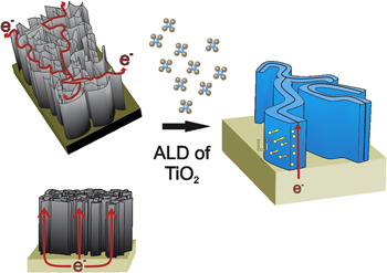
Figure 1. Schematic of electron conduction in carbon nanosheets and their use as a 3D substrate for TiO2. The fast electron transport and short Li+ diffusion path leads to a high-power density.
Download figure:
Standard image High-resolution imageIn this work, we studied the balance between performance and capacity as a function of a different thickness (15–25 nm) of the ALD deposited amorphous TiO2 on substrate-attached CNS. A remarkable rate capability and stable cyclic performance is achieved. It is shown that the film thickness of TiO2 has an effect on the kinetics of the Li+ storage mechanism. Furthermore, the fabrication steps involved in this work are compatible with existing microfabrication and processing techniques for integrated microsystems.
2. Experimental details
2.1. Preparation of vertically standing CNS on TiN/Si substrate
A 200 mm silicon wafer with 90 nm thermal SiO2 coated with 70 nm TiN was used as the carrier for deposition. The TiN layer was deposited by sputtering from a Ti target in a N2 atmosphere (Applied Endura Extensa TTN). The TiN layer served as the electrical contact to the CNS and lithium diffusion barrier for the underlying Si. CNS films were grown in a PECVD chamber capacitively coupled with an RF (13.56 MHz) source (Oxford Instruments Plasma Technology, UK). In brief, the growth of the CNS was initiated by heating the TiN-covered wafer to 750 °C under vacuum (10−6 mbar) for 1 min. An H2 plasma pre-treatment (300 W) was carried out for 15 min at 0.6 mbar. C2H2 was added to the H2 plasma at a 1:10 ratio (C2H2:H2) for 45 min. The CNS-covered wafer was removed from the chamber and allowed to cool under vacuum (10−4 mbar) for 5 min.
2.2. ALD of TiO2 on CNS
Different samples were cleaved from the CNS-covered wafer in 2 × 2 cm pieces and loaded into a home-built ALD reactor with a base pressure of 5 × 10⁻⁷ mbar. Before starting the ALD cycles, the sample was heated to 100 °C and kept at this temperature for 1 h. One ALD cycle of TiO2 consisted of alternately applying a pulse of tetrakis(dimethylamido)titanium (TDMAT) (99.999% Sigma-Aldrich) at 3 × 10⁻¹ mbar and a pulse of ∼150 μg mL−1 ozone (produced by ozone generator, Yanco Industries, LTD) at 5 × 10⁻¹ mbar for 20 s each. To completely remove all of the residual gases between each precursor pulse, the reactor was evacuated for 40 s to a pressure of 1 ∼ 2 × 10⁻⁵ mbar. By varying the amount of cycles (i.e. 300, 400 and 500 cycles), different thicknesses of TiO2 were deposited on the CNS. To determine the influence of the CNS and TiO2 separately, TiO2 was also grown using the same amount of cycles without CNS on the TiN substrate.
2.3. Structural characterization
X-ray diffraction (XRD) was performed on a Bruker D8 System Diffractometer equipped with Cu Kα radiation by scanning in the 2ϑ range in the grazing incidence mode. The TiO2/CNS films were analysed by scanning electron microscopy (SEM) and Raman spectroscopy (Jobin-Yvon spectrometer, 0.3 cm−1 spectral resolution, laser power of 0.5 mW). The equivalent thickness of the TiO2 after 300, 400 and 500 ALD cycles was determined by x-ray fluorescence (XRF) measurement (ARTAX system, Bruker) of the Ti content.
2.4. Electrochemical testing of TiO2/CNS electrodes
Electrochemical measurements were performed using a custom-built three-electrode glass cell. The glass cell was clamped onto 2 cm × 2 cm samples using a Viton O-ring. The geometrical surface area of the exposed electrode was 1.43 cm2. A lithium metal sheet and a wire were used as a counter and reference electrode, respectively. The Li reference electrode was placed in a glass capillary with the tip placed less than 1 mm from the electrode surface. Contact was made to the bare TiN underlayer with a crocodile clip at the edge of the sample (outside of the glass cell). The electrolyte used was 1.0 M LiPF6 in a 50:50 (v/v) mixture of ethylene carbonate (EC) and diethyl carbonate (DEC) (LP40, Merck). All of the operations on the cell assembly were carried out in a glove box (Inert Lab) filled with argon gas in which both the water and oxygen concentrations were less than 1 ppm. A potentiostat/galvanostat Autolab PGSTAT30 (Metrohm Autolab) was used to perform all of the electrochemical experiments, which were controlled through Nova 1.8 software. All of the voltages are given versus the Li+/Li.
Cyclic voltammograms (CV) were recorded starting from the open-circuit potential between 3.00 V and 0.01 V at different scan rates (0.5–500 mV s−1). Subsequently, galvanostatic cycling was performed between 3.00 V–0.01 V at various current densities (C-rates) to evaluate the rate and cycle performance. For the charging rate, 1 C was determined based on the charge calculated from the discharge capacity with a 0.5 mV s−1 CV.
3. Results and discussion
3.1. Structure and morphology of the as-prepared and TiO2-coated CNS
The SEM images of the as-prepared and ALD TiO2-coated CNS on the TiN/SiO2/Si substrate is shown in figure 2. The top-down SEM image (figure 2(a)) shows the corrugated petal-like arrangement of the as-prepared CNS that leads to its high surface to volume ratio. A Raman spectrum of the as-prepared CNS is shown in figure S1 and exhibits well-distinguished D and G peaks together with second-order peaks. A peak intensity ratio ID/IG [17] of 2.6 indicates that the sheets are defective, with an average crystallite size (La) of 2.68 nm, indicating at the very least that there are sites available every 2.68 nm along the edge and basal surface of a 700 nm sheet where nucleation of ALD deposited TiO2 can take place. A detailed description of the Raman spectral behaviour of surface-attached CNS can be found in [4].
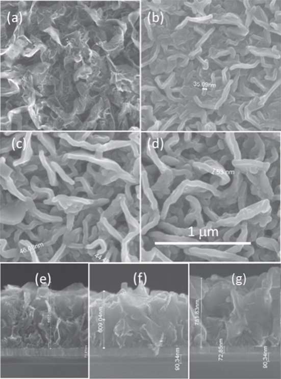
Figure 2. SEM images of bare CNS and TiO2-CNS; (a) top view of bare CNS; (b) top view of 15 nm TiO2-CNS, (c) 20 nm TiO2-CNS and (d) 25 nm TiO2 on CNS; (e–g) side view of 15, 20 and 25 nm TiO2-CNS.
Download figure:
Standard image High-resolution imageAfter TiO2 deposition, the resulting surface morphology can be seen in the top view SEM image of figures 2(b)–(d). By varying the number of ALD cycles between 300 (figure 2(b)), 400 (figure 2(c)) and 500 (figure 2(d)) cycles, a different thickness of TiO2 on the CNS composite was obtained. Figures 2(e)–(g) also show the cross-section SEM image for 300, 400 and 500 ALD TiO2 on CNS, showing a height of ∼600–750 μm and the coverage of the TiO2 inside of the CNS structure. The top-view SEM images of figures 2(b)–(d) give a rough estimate of the thickness of the TiO2/CNS/TiO2 sheets. For 300 cycles of ALD, the thickness is ∼35 nm, which increases for 400 and 500 cycles of ALD to ∼50 and ∼60 nm, respectively. This is roughly in accordance with the nominal thickness of TiO2 based on the ALD growth rate of a 0.05 nm/cycle for a CNS thickness of 10 nm and takes into account that the TiO2 can deposit on both sides of the exposed CNS (see table 1). The equivalent thicknesses of deposited TiO2 for different ALD cycles based on the Ti content have also been obtained from XRF measurements and are given in table 1.
Table 1. Thickness of the TiO2 determined with different techniques with the corresponding area enhancement and theoretical capacity.
| # of ALD cycles | Equivalent thickness TiO2 from XRF signal (nm) | Theoretical capacity of LixTiO2 for x = 1 (μAh cm−2) | Thickness TiO2 estimated from growth ratea (nm) | Conformal thickness estimated from top-down SEMb (nm) | Area enhancementc |
|---|---|---|---|---|---|
| 300 | 133 | 19 | 15 | 13 | 9 |
| 400 | 213 | 30 | 20 | 20 | 11 |
| 500 | 238 | 34 | 25 | 25 | 10 |
aFor a growth rate of 0.05 nm/cycle. bFor CNS of ∼10 nm in thickness and for TiO2 coated on both sides of the CNS. cRatio of equivalent/conformal thickness.
The equivalent thickness is the thickness for a dense planar TiO2 film (∼4.2 g cm−3) that is equivalent to the total amount of measured Ti by XRF on the sheets. Using this value, we also calculated the theoretical capacity of equivalent films with these thicknesses, also summarised in table 1. The ratio of the equivalent thickness and actual conformal thickness gives us the area enhancement of the CNS structures, which is ∼10 in all cases. The consistency in conformal thickness and area enhancement points toward a good conformal coating of the TiO2 on the CNS, even though we cannot exclude pinholes and weak spots as a result of the initial nucleation and growth, especially deep down in the pores or at the folded sheets.
The XRD measurements did not show any TiO2 signal, which points to the amorphous nature of the TiO2. This can be explained by the relatively low deposition temperature of 100 °C. Although the use of amorphous TiO2 is less known in literature compared to anatase, we found that it shows excellent lithium storage properties, which will be elaborated on in the next section. From here on, the 300, 400 and 500 cycle TiO2 on the CNS will be named 15 nm TiO2-CNS, 20 nm TiO2-CNS and 25 nm TiO2-CNS.
3.2. Electrochemical activity of TiO2/CNS
Cyclic voltammetry at various scan rates was employed to study the kinetic properties of 15, 20 and 25 nm TiO2-CNS. Figure 3(a) shows the third cyclic voltammograms (CV) at a scan rate of 0.5 mV s−1 in the voltage window of 3.00-0.01 V for bare CNS on TiN and the different TiO2-CNS samples. A sharp reduction peak can be seen for the bare CNS around 0.1 V and a slightly broader oxidation peak around 0.2 V can also be seen, which is in accordance with earlier reports on CNS [6]. In figure 3(a), it can also be seen that for all three types of TiO2-CNS, a broad reduction and oxidation peak around 1.5 V is measured, which is related to the insertion and extraction of the Li+ in TiO2, respectively. Broad peaks in the CV is an indication of homogeneous filling of TiO2 with the absence of an immiscible two-phase region; the same response has recently been measured with amorphous TiO2 nanotubes [18] and porous nanostructured amorphous TiO2 films [19]. Furthermore, for 15 and 20 nm TiO2-CNS, an additional oxidation peak is measured around 0.7 V; this is likely due to the signal from the CNS which, in the case of the oxidation peak, is shifted to more positive potentials. This oxidation peak seems to only be available for TiO2 samples with a thin enough coverage of TiO2, suggesting that a thicker layer will block the lithiation/delithiation of the underlying CNS.

Figure 3. The third cyclic voltammograms (a) of bare CNS and of 15, 20 and 25 nm TiO2-CNS at 0.5 mV s−1, (b) of 15, 20 and 25 nm TiO2-CNS at 10 mV s−1 and (c) of planar 15, 20 and 25 nm TiO2 on TiN at 10 mV s−1.
Download figure:
Standard image High-resolution imageAt a higher scan rate of 10 mV s−1 (figure 3(b)), several changes in the response of the different TiO2-CNS samples is seen. The peak current density of 20 nm TiO2-CNS is higher compared to that for 15 and 25 nm TiO2-CNS. Also, the peak potential difference is lowest for 20 nm TiO2-CNS and highest for 25 nm TiO2-CNS; this indicates an increased overpotential needed for the insertion/extraction. Additionally, a small shoulder can still be seen below 1.0 V, which can be attributed to the underlying CNS; however, it has increased overpotential for delithiation. As a reference, TiO2 was deposited on TiN with thicknesses of 15, 20 and 25 nm, and a CV was recorded at 10 mV s−1 (see figure 3(c)). This also showed the broad characteristic oxidation/reduction peaks for TiO2 around 1.5 V, with an additional shoulder at 1.2 V, which has not yet been identified. However, ongoing tests suggest that this shoulder is related to the amorphous TiO2.
The CNS template provides a large surface area for the ultra-thin TiO2 electrode. Increasing the thickness of TiO2 can impede the accessibility of the electrolyte into the TiO2/CNS pores. This in turns affects the diffusion mechanism, which in turn affects the charge stored. The apparent diffusion mechanisms can be examined by analysing the peak currents versus the scan rates of the recorded CVs. Figure 4(a) shows the cathodic peak current associated with lithium extraction from TiO2 as a function of the scan rate (0.5–500 mV s−1) determined from CVs measured for different TiO2-CNS samples. A similar result is obtained for the anodic peak current. The current measured obeys a power law relation with the sweep rate,

where a and b are adjustable parameters. The slope of log i versus the log v plot gives the b value. A value of b close to 0.5 is an indication of a semi-infinite diffusion controlled reaction, while b close to unity indicates a surface controlled reaction [20]. Here, the b value obtained for 15, 20 and 25 nm TiO2-CNS electrodes are 0.74, 0.75 and 0.56, respectively. The 15 and 20 nm TiO2-CNS exhibits a mixed surface and semi-infinite diffusion controlled response, whereas the current response for the thicker layer of TiO2 on the CNS shows semi-infinite length diffusion behaviour.
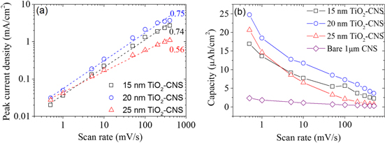
Figure 4. (a) Peak current densities of lithium extraction from different TiO2 thicknesses on CNS as a function of the scan rate. The dotted line shows the slope with the corresponding b value. (b) The extracted capacity of delithiation (discharging) for the different TiO2 thicknesses on CNS and bare CNS.
Download figure:
Standard image High-resolution imageThe reason as to why 20 nm TiO2-CNS shows an optimum in terms of capacity and rate performance can be explained by the optimal balance between the available amount of active material (in this case, TiO2), the accessibility of the liquid electrolyte inside the pores of the whole nanostructure and the availability of the underlying CNS, which can also be active. Figure 5 shows a schematic that illustrates the different situations when increasing the TiO2 thickness. More active material becomes available with the increased film thickness. Below a certain thickness (≤20 nm), the nanostructure allows for good penetration of the electrolyte, which in turn allows short diffusion distances for Li+ transport (≤20 nm). In this case, increasing the TiO2 thickness will lead to more capacity, as can be seen in the increase in capacity from 15 to 20 nm TiO2-CNS in figure 4(b). However, when a certain TiO2 thickness is reached (>20 nm), the pores become clogged, allowing only the top of the TiO2-CNS to be in contact with the electrolyte. The lack of electrolyte penetration significantly diminishes the rate at which the structure can be charged since Li+ has to be transported from the electrolyte-TiO2 interface all the way through the solid TiO2-CNS (≈0.6 μm) structure.

Figure 5. Schematic of lithium insertion into TiO2-CNS showing the influence of the increased TiO2 thickness. When the TiO2 thickness is below a certain threshold, the TiO2-CNS electrode allows for penetration of the electrolyte and offers a short diffusion length for Li+ transport in TiO2. However, above this threshold, the pores are closed off, and the electrolyte cannot penetrate the composite electrode, thereby significantly increasing the Li+ diffusion length, which leads to a lower capacity and to lower rate performance.
Download figure:
Standard image High-resolution imageAs a reference, bare CNS were also measured, and the capacity as a function of the scan rate was also plotted in figure 4(b). This clearly shows the importance of using TiO2 combined with CNS; at 0.5 mV s−1, the capacity of a 1 μm tall bare CNS is 2.4 μAh cm−2, which is an order of magnitude less than the capacity of 20 nm TiO2-CNS. This can be explained by the highly porous (∼70% free space [4]) structure of the CNS, which has very little active material for a given geometric surface area; this is often ignored when normalizing by weight, as is typically done in literature [5, 6, 15].
3.3. Galvanostatic charge/discharge characteristics of CNS and TiO2/CNS
The effect of the TiO2-coating thickness on the capacity was also determined by performing galvanostatic charge/discharge experiments. The C-rate was experimentally determined based on the delithiation charge measured during the CV at 0.5 mV s−1 (see figure 4(b)), which was calculated for 1 C to be 17.5, 24.5 and 19.6 μA cm−2 for 15, 20 and 25 nm TiO2-CNS, respectively. Figure 6(a) shows the discharge curves obtained from TiO2-CNS between the voltage ranges of 3-0.01 V at a rate of 0.1 C. Distinctive voltage regions below and above 1 V are seen for 15 and 20 nm TiO2-CNS, whereas the whole discharge capacity of 25 nm TiO2-CNS is mainly achieved above 1 V. The discharge capacities obtained at 0.1 C (discharging in 10 h) for 15, 20 and 25 nm TiO2-CNS are 26 μAh cm−2, 38 μAh/cm2 and 17 μAh cm−2, which is 137%, 127% and 50% of the theoretical TiO2 capacity of a film, with the equivalent thicknesses given in table 1, respectively. Note that we have taken the full theoretical capacity of the 1 Li+ per TiO2 unit formula instead of ∼0.6 Li+, which is usually done in literature. The capacities obtained are above the theoretical ones and are attributed to the insertion of Li+ into the underlying CNS, which also participates at voltages below 1.0 V. As mentioned above, the C-rate was experimentally determined; however, this rate can be compared to the theoretical current density based on the complete lithiation/delithiation of the total amount of TiO2 present (see table 1). To charge the different TiO2-CNS samples in 1 h using the theoretical capacities from table 1, we would need to apply 19, 30 and 34 μAh cm−2 for 15, 20 and 25 nm TiO2-CNS, respectively. The actual current density applied is 93%, 82% and 58% of this theoretical one. It indicates that the current density applied for 15 and 20 nm TiO2-CNS is close to the theoretical one, except for the 25 nm TiO2 in which a slightly lower current density compared to the theoretical one was applied. This suggests more time was available for lithium transport in this sample compared to the 15 and 20 nm TiO2-CNS ones. Taking this into account, 25 nm TiO2-CNS clearly has the lowest measured capacity and the lowest rate performance and utilization of the TiO2 content.
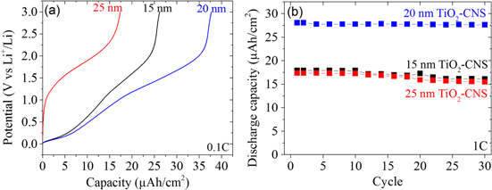
Figure 6. (a) Galvanostatic discharge at 0.1 C and (b) a cycling test at 1 C for 30 cycles of 15, 20 and 25 nm TiO2-CNS. The applied current at 1 C for the different samples was 17.5, 19.6 and 24.5 μA cm−2 for 15, 20 and 25 nm TiO2, respectively.
Download figure:
Standard image High-resolution imageThe cycling of the TiO2-CNS anodes was evaluated up to 30 charge/discharge cycles and is given in figure 6(b). All of the TiO2-CNS samples show excellent capacity retention with minimum capacity loss. The 20 nm TiO2-CNS retained a discharge capacity of 27.6 μAh cm−2 in the 30th cycle, which is about 98% of the initial value. For the 15 and 25 nm TiO2-CNS, the capacity retention is slightly less than for the 20 nm TiO2-CNS, which shows a retention of about ∼90% of the initial value in both cases after 30 cycles. SEM images taken (see figure S2) of 15 nm TiO2-CNS after cycling showed no noticeable change to the TiO2-CNS structure. In some regions, deposits on top of the whole TiO2-CNS structure were seen, which could either be the formation of an SEI or salt deposits formed during drying of the residual electrolyte after disassembly of the cell. Longer term cycling (>30 cycles) experiments would be needed to determine possible failure mechanisms since no sudden drop in capacity was observed in our case.
3.4. Rate capabilities
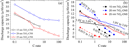
In order to demonstrate the high-rate capability of the TiO2/CNS anode, galvanostatic charge/discharge tests were performed at various charging rates. Figure 7(a) shows the discharge capacity of the three different TiO2-CNS samples with varying current rates ranging from 0.1 C to 100 C. The discharge capacity of 15 and 25 nm TiO2-CNS at 100 C is ∼50% and ∼4% of the 0.1 C capacity, respectively, and 20 nm TiO2-CNS retains 47% of the original capacity at 5 C. It is clear that 20 nm TiO2-CNS possesses the highest capacity at very high C-rates among the three different TiO2-CNS, highlighting the excellent rate capabilities of this TiO2/carbon nanosheet hybrid. In order to discern the capacity associated between the TiO2 and the CNS, the capacity as a function of the C-rate was plotted for two voltage ranges in figure 7(b) (from 0.01 V to 1.0 V and from 1.0 V to 3.0 V). For all three TiO2-CNS samples, as the charging rate increases, a smaller amount of capacity is associated with the voltage region below 1.0 V, suggesting that the extraction of Li from the CNS is not possible at higher current rates. The 20 nm TiO2-CNS seems to have, overall, more capacity associated to the low voltage region and retains a larger amount of capacity as a function of the C-rate for the high voltage region.
Figure 7. Rate performance of the different TiO2-CNS samples showing the delithiation (discharge) capacity as a function of the C-rate. (b) The discharge capacity was taken in two different voltage ranges, from 0.01 V to 1.0 V and from 1.0 V to 3.0 V, for the different TiO2-CNS samples.
Download figure:
Standard image High-resolution image
There was good reproducibility of these results, showing consistently that the 20 nm TiO2-CNS is superior. This can also be confirmed by comparing the capacities measured with different samples of the same thickness. For example, the capacities at 1 C in figure 6(b) are 17, ∼28 and 16 μAh cm−2 for 15, 20 and 25 nm TiO2-CNS, respectively. The capacities shown in figure 7(a) at a rate of 1 C gave very similar results and allow for a direct comparison since it concerns different samples of the same TiO2 thickness.
4. Conclusions
We have prepared nanostructured amorphous TiO2 composite electrodes with 300, 400 and 500-cycle ALD on CNS templates and have evaluated the electrochemical performance as the anode layer of LIB. The ALD deposition leads to an area enhancement of factor ∼10 in all cases, with a nominal coverage of 15, 20 and 25 nm on the petal-like corrugated CNS structure. The CNS template functions as an electronic conductive layer and also as the lithium insertion host, giving mechanical support and an increased surface area for the TiO2. Cyclic voltammetry showed fast kinetics for the 15 and 20 nm TiO2-CNS in contrast to the 25 nm TiO2-CNS, and the highest capacity was found for 20 nm TiO2-CNS. This was also confirmed with galvanostatic charge-discharge experiments at 0.1 C, which showed capacities of 26, 38 and 17 μAh cm2 for 15, 20 and 25 nm TiO2-CNS, respectively. The rate performance was probed up to 100 C (charging in 36 s), at which point the 20 nm TiO2-CNS showed the best performance with a capacity of 19 μAh cm−2, retaining 47% of its original capacity. The cycleability of the electrodes were tested by cycling at 1 C and showed a capacity retention after 30 cycles of ∼98% for the 20 nm TiO2-CNS compared to ∼90% for the 15 and 25 nm TiO2-CNS.
The results highlight the importance of depositing a TiO2 film with a thickness tailored to the CNS substrate, as too thin of a TiO2 film will not effectively use the open space between the CNS, which lowers the overall capacity; too thick of a film will block adequate penetration of the electrolyte inside of the pores, hampering the kinetics, which in turn hampers the capacity. The optimal film thickness is found with a 20 nm TiO2-CNS TiO2/carbon nanosheet hybrid, offering the best in terms of capacity, rate-performance and cycleability. These results show the potential of TiO2-CNS as a robust and high rate performing electrode. Finally, the IC compatible fabrication steps make possible the integration of TiO2-CNS electrode material for other micropower applications.
Acknowledgments
The authors are thankful for the financial support of IWT-Vlaanderen through the SBO-SOSLION and LAMINALION projects. CD acknowledges the European Research Council for providing funding (FP7/2007-2013, ERC grant agreement n 239865) and UGent-BOF for providing funding through GOA-01G01513.