
Abstract
Thin film or porous membranes made of hollow, transparent, conducting oxide (TCO) nanotubes, with high chemical stability, functionalized surfaces and large surface areas, can provide an excellent platform for a wide variety of nanostructured photovoltaic, photodetector, photoelectrochemical and photocatalytic devices. While large-bandgap oxide semiconductors offer transparency for incident light (below their nominal bandgap), their low carrier concentration and poor conductivity makes them unsuitable for charge conduction. Moreover, materials with high conductivity have nominally low bandgaps and hence poor light transmittance. Here, we demonstrate thin films and membranes made from TiO2 nanotubes heavily-doped with shallow Niobium (Nb) donors (up to 10%, without phase segregation), using a modified electrochemical anodization process, to fabricate transparent conducting hollow nanotubes. Temperature dependent current–voltage characteristics revealed that TiO2 TCO nanotubes, doped with 10% Nb, show metal-like behavior with resistivity decreasing from 6.5 × 10⁻⁴ Ωcm at T = 300 K (compared to 6.5 × 10⁻¹ Ωcm for nominally undoped nanotubes) to 2.2 × 10⁻⁴ Ωcm at T = 20 K. Optical properties, studied by reflectance measurements, showed light transmittance up to 90%, within wavelength range 400 nm–1000 nm. Nb doping also improves the field emission properties of TCO nanotubes demonstrating an order of magnitude increase in field-emitter current, compared to undoped samples.
Export citation and abstract BibTeX RIS
1. Introduction
Transparent conducting oxides (TCOs) combine electrical conductivity and optical transparency that plays an important role in modern optoelectronic applications [1, 2]. Moreover, the high chemical stability of oxides, ability to functionalize the surface easily, large surface areas for hollow nanotubes, and optimal alignment of energy states for charge extraction, makes TCO nanotubes an excellent platform for nanostructured light absorption/emission and catalytic applications. Recently, several groups have been developing Indium-tin-oxide (ITO) nanowires for nanostructured light emitting diodes and photovoltaic applications [3–5]. However, optimal band alignment of titanium dioxide (TiO2) for charge injection/extraction with a wide range of semiconductors, and application as a photoelectrochemical, photocatalytic, and photovoltaic material [6–8] makes it an ideal candidate for TCO applications, for easy integration in wide variety of nanostructured devices. Moreover, due to it's low cost, abundance (application of ITO as TCO thin films [2] has resulted in scarcity of natural indium supply), high chemical stability, and low toxicity of anatase TiO2, it can be an important TCO nanotube material [6–10]. Here, we demonstrate for the first time, TiO2 TCO nanotubes using shallow Niobium (Nb) dopant, fabricated using a modified electrochemical anodization process. We report TCO nanotubes with high charge carrier concentrations (>3 × 1021 cm−3), large conductivity (1.54 × 10³ Scm−1), high transmittance (up to 90% between 400–1000 nm) and good field-emission properties.
We chose Nb as the shallow electron dopant for anatase TiO2 because of it's low ionization energy (4–30 meV [11–15]), high solubility [13], and similar ionic radius as Ti4+ (r(Ti4+) = 0.605 Å versus r(Nb5+) = 0.64 Å) [16]. Nb acts as a substitutional dopant for Ti and donates excess electron to the conduction band, forming strong hybridized 4d orbitals with the 3d orbitals of Ti [17]. Using epitaxial thin films of Nb-doped anatase TiO2 (formed on SrTiO3 or LaAlO3 single crystalline substrates by pulsed laser deposition), it was recently shown that low electrical resistivity (2.1 × 10⁻⁴ Ωcm) and high internal transmittance (>90%, in the visible region) can be achieved [2, 13]. However, heavy doping of nanoscale structures has proven more challenging, due to large surface area, reduced dimensions for ejection of dopants, and high diffusivities [18–20]. A number of methods like post-growth ion implantation, thermal annealing, or using metal alloys as initial anodization material, have been tried for doping of TiO2 nanotubes [21]. However, none of these methods has been able to achieve heavy doping levels (>1021 cm−3) required for TCO performance. Our new doping method using modified electrochemical anodization process, allows facile fabrication of undoped and doped widebandgap oxide nanotubes, with varying doping levels (from light doping to heavily doped nanotubes, >1021 cm−3).
2. Experimental
TiO2 nanotube growth was performed using anodization method [22–29]. Electrolyte consisted of solvent (ethylene glycol) with 1% ammonium fluoride (NH4F), and 2% of water. 1'' × 1'' sized Titanium (Ti) sheets were for anodization and investigation by different characterization techniques. For the anodization process, Ti sheet and platinum (Pt) electrode were immersed in the electrolyte 2–3 cm apart. The growth rate of nanotubes in ethylene glycol was approximately ∼4 μm h-1. All as-grown samples were amorphous and they were annealed at 500 °C for 1 h in air to convert to anatase phase. Doping to form TCO nanotubes was performed using modified electrochemical cell, with two sections separated by a porous membrane, and using alternating current cycles. The new modified electrochemical cell with Pt electrode is filled with electrolyte (described above) free of dopant precursor. The second section with Ti anodization sheet is filled with electrolyte that contains dopant precursor. The porous membrane is semi-permeable to the electrolyte, and serves as the physical barrier between two sections of the electrochemical cell (to prevent mixing), while still allowing flow of electrolyte to complete the cell.
For doping the TCO nanotubes with Nb, NbCl5 was added as a dopant precursor in the electrolyte. We found a linear relationship between the amount of precursor added (NbCl5 wt%) in electrolyte and the detected Nb dopant concentration in TCO nanotubes. For comparison, the undoped sample was also grown and studied along with doped samples. Anodization voltage, which determined the nanotube diameter [24, 27], was set to 30 V during growth for all samples. This was done to ensure similar nanotube diameter, thickness and other morphological parameters constant, except the dopant concentration in TCO nanotubes. This allowed us to study the effect of doping on TCO nanotubes properties. The nanotube diameter using this anodization process (30 V applied voltage) was ∼80 nm (figure 1(a)). The growth time, which determines the nanotube height, was also kept constant in subsequent measurements to 30 min; and the corresponding nanotube carpet height was ∼2 μm (figure 1(b)).

Figure 1. (a) and (b) SEM images of nanotubes grown by electrochemical oxidation: a—top view, b—side view. To eliminate effects arising from geometry, all samples had same nanotube diameter (∼80 nm), wall thickness (∼10–15 nm) and height of nanotube carpet (∼2 μm). (c) XRD pattern for undoped TiO2 nanotubes; (d) An XPS spectrum obtained for undoped TiO2 nanotubes. Only reflection peaks corresponding to anatase TiO2 were observed in all samples without any corresponding to secondary phases. Peaks marked 'Ti' in the 2θ patterns in this figure correspond to the underlying Ti substrate from which TiO2 nanotubes were grown. Reflection peaks (101) and (200) at 2θ = 25.3° and at 47.95° correspond to anatase phase.
Download figure:
Standard image High-resolution imageThe morphology of the grown TCO nanotubes was examined in field-emission scanning electron microscope FE-SEM JEOL 7401F. Compositional analysis were performed by energy dispersive x-ray spectroscopy (EDS) embedded in the same FE-SEM instrument. The EDS analysis were performed in different modes (2D mapping, point scan, etc) to test for uniformity and possible secondary phases (Niobium oxide Nb2O5, metallic Nb, etc). Quantification of Nb concentration in TCO nanotubes performed using INCA software (Oxford Instruments) integrated with FE-SEM, which used measured EDS spectra and a calibration table, to calculate the percentage of constituent elements. For Nb dopant, we utilized the Lα radiation (2.166 KeV) generated by the scanning electron beam. The crystal structure of doped and undoped TiO2 nanotube samples were analyzed by x-ray diffraction (XRD) measurements using a Scintag XDS 2000 x-ray diffractometer. The measurements were performed using Cu Kα radiation at 45 kV and 40 mA.
I–V characterization was performed by two different ways: (1) from single nanotubes using current-sensing atomic force microscopy (CS-AFM) and (2) ensemble measurements using Keithley source meter (Keithley 2612A, Tektronix). CS-AFM I–V was used for resistivity measurements, while ensemble measurements were used for temperature dependent current–voltage characterization (I–V–T). The setup configuration for ensemble measurements was similar to that for CS-AFM (TCO nanotubes sandwiched between metal contacts). In CS-AFM measurements, ∼6 nm contact radius with a nanoscaled tip was used, while in case of ensemble measurements the contact radius of the metal probe was ∼100 μm.
I–V–T measurements were performed in temperature range 20 K–300 K, with 10 K temperatures steps, using a closed loop Helium Cryostat (ARS-202AE with ARS-2HW Helium compressor, Advanced Research Systems). The voltage used for these measurements was varied in the range −20 V to +20 V. Sheet resistance of nanotubes R was calculated from I–V measurements using Ohm's law  . Then, resistivity
  was calculated using equation
  , where L is nanotube length, and A—total nanotube contact cross-sectional area.
Reflection measurements were performed in the wavelength range 400–1000 nm using a home-built confocal optical microscope. The confocal setup used an inverted microscope (AXIO-Observer, Zeiss), series of confocal pinholes, a 400 μm fiber optical cable, and the collected UV-Vis absorption spectrum was measured on an Ocean Optics USB4000 spectrometer with resolution of ∼0.1 nm.
Scanning Tunneling Microscope (STM) characterization was done using a customized Molecular Imaging PicoScan 2500 setup (with PicoSPM II controller). An STM nosecone (N9533A series, Agilent Technologies) was used for scanning and spectroscopy using chemically etched Pt–Ir tips (80:20). The measurements were done at room temperature under atmospheric conditions. Tunneling junction parameters were set at tunneling currents ranging between 100 and 500 pA and sample bias voltage between −5 and +5 V. The tunneling current as a function of applied bias voltage (STS) was recorded at multiple positions on the sample. A modified Molecular Imaging PicoSPM setup was used for current sensing AFM (CS-AFM) measurements. The CS-AFM tips used were coated in-house using thermal evaporator with 5 nm of 99.99% Cr and 15 nm of 99.99% Au. Multiple current scans were taken at different bias voltage ranging from −5 to +5 V.
X-ray photoelectron spectra (XPS) of TiO2 samples were obtained using a PHI 5600 x-ray photoelectron spectrometer. The nanotube powder samples were collected from the TiO2 nanotube sample by scraping. Monochromatic Al Kα x-rays (1486.6 eV) were used for the XPS analysis. The pass energy was 93.9 eV and the step size was 0.400 eV. An electron beam neutralizer was employed at 17.8 mA. Data was collected with Auger Scan (RBD Enterprises, Bend, OR). XPS data was analyzed in CASA XPS (Casa Software, UK). Quantitative measurement of TiO2 samples was performed with an ARL 3410+ inductively coupled optical emission spectrometer (ICP-OES).
3. Results and discussion
Morphological characterization and elemental mapping of TCO nanotubes reveal uniform incorporation of Nb dopant in the TiO2 nanotube matrix. Scanning electron micrographs (SEM) (figures 1(a), (b)) showed (a) nanotube diameter (top view), and (b) cross-section SEM images of TCO nanotubes grown during experiments. The hollow tubular structure of nanotubes is well preserved after doping (method described above). The nanotube diameter and height of all samples studied in this work was ∼80 nm and 2 μm, respectively (to eliminate geometrical effects). The anodization voltage used for their growth was 30 V and the growth time was 30 min. The wall thickness was ∼10–15 nm. All samples had anatase phase, that was confirmed from XRD patterns (figure 1(c)) and XPS spectrum (figure 1(d)). XRD pattern showed reflection peaks corresponding to anatase phase with predominant peaks (101) and (200) at 2θ = 25.3° and at 47.95°, respectively. XPS spectrum revealed anatase O1 s and Ti2p3/2 peaks. The XRD pattern of doped samples did not change with doping level up to 11%, ruling out phase segregation and formation of other secondary phases even at high doping levels. In figure 2(a), XRD patterns for Nb doped TiO2 nanotubes with doping level up to 11%, shows only reflection peaks corresponding to anatase TiO2 with no peaks corresponding to any secondary phase (possibly due to formation of unintentional niobium oxide (Nb2O5) or other metallic Nb crystallites).
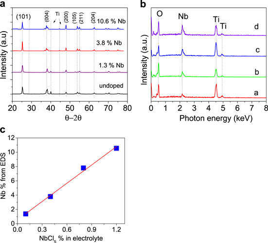
Figure 2. (a) XRD patterns for undoped and Nb doped TCO nanotubes, with different Nb concentrations. Peaks marked 'Ti' in the 2θ patterns in this figure correspond to the underlying Ti substrate from which TiO2 nanotubes were grown; (b) EDS spectra of different TCO nanotubes prepared with different amount of NbCl5 in the electrolyte: 0.1%, 0.4%, 0.8%, and 1.2%; (c) Nb concentration in nanotubes, detected by EDS, as a function of NbCl5 concentration in electrolyte.
Download figure:
Standard image High-resolution imageEDS analysis confirmed presence of doped elements in TiO2 nanotubes as shown in figures 2(b), (c). TCO nanotube samples were prepared with different amount of NbCl5 in the electrolyte: 0.1%, 0.4%, 0.8%, and 1.2% shown in figures 2(b), (c). The corresponding Nb concentration in TCO nanotubes, quantified using EDS, were 1.37%, 3.8%, 7.8%, and 10.55%, respectively, presenting a linear relationship between the amount of incorporated dopants in TiO2 nanotubes and the NbCl5 precursor concentration in the electrolyte (figure 2(c)). The conductivity of Nb-doped TiO2 nanotubes increased (resistivity decreased) with wt% NbCl5 precursor (see discussion below), further confirming the incorporation of electronic Nb dopant into TiO2 crystal. To further confirm uniform incorporation of Nb dopant along each nanotube, EDS point scans were taken from different locations on a individual Nb doped TiO2 nanotube. The point scan was performed by focusing an electron beam onto the wall of single nanotube, and recording the corresponding EDS spectra. The results showed uniform distribution of Nb over the entire length of the nanotube (figure 3(a)).
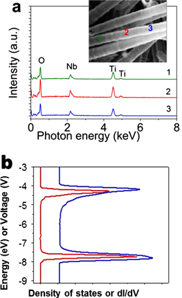
Figure 3. (a) EDS from a single nanotube point scan, performed by pointing a focused electron beam onto the surface of individual nanotubes (shown in inset). The representative point scan (taken over several points along the hollow TCO nanotube walls) demonstrates uniform incorporation of Nb into TiO2 crystal lattice. (b) Scanning tunneling spectroscopy for undoped (red curve) and Nb doped TCO (blue curve) nanotubes. Nb doping level for TCO nanotubes was 10.6%.
Download figure:
Standard image High-resolution imageTo further test the change in electronic density of states (DOS) of TiO2 nanotubes due to incorporation of Nb dopants, and measure the resulting donor level created in the electronic spectra, we conducted STS analysis of the doped samples. STM characterization confirmed the presence of Nb in TiO2 nanotubes and revealed new uniform shallow DOS near the conduction band of Nb-doped TiO2 nanotubes (figure 3(b)). The Fermi level in TCO nanotubes is very close to the bottom of conduction band, indicating n-type conductivity (figure 3(b)). Comparison between the DOS for undoped TiO2 and TCO nanotubes (figure 3(b)) also shows that Nb is likely a shallow donor, which does not produce any additional states within the bandgap of TiO2 semiconductor (maintains transparency). Therefore, STS analysis confirmed incorporation of electronically active shallow Nb dopant, change in electronic DOS of doped TiO2 nanotubes, and likely transparency of the doped TCO nanotubes.
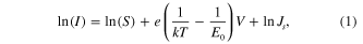
Electronic properties of single TCO nanotubes were studied using CS-AFM. I–V characterization of single nanotubes was conducted, using a sharp conductive (gold-coated) AFM tip to make electrical contact with single hollow vertically aligned TiO2 nanotubes and the open area of Ti sheet as the second contact to form complete circuit. Figure 4(a) illustrates the experimental configuration used for the CS-AFM measurements. Using I–V characteristics for Nb doped and undoped TiO2 nanotubes, the resistivity, ρ, of individual nanotubes was calculated (using R = ΔV/ΔI, and  , where L is length of nanotubes, S is contact area of the tip). The measured resistivity for 1% Nb doped nanotubes was found to be 2.3 × 10⁻³ Ωcm, which is two orders of magnitude smaller than the resistivity of undoped nanotubes 6 × 10⁻¹ Ωcm. The resistivity of the doped samples decreased with an increase of Nb concentration, and approached 6.5 × 10⁻⁴ Ωcm for 10% Nb doped TiO2 nanotubes (figure 4(b)). The increase of conductivity (1/ρ) of Nb-doped TCO nanotubes was expected due to ionization of Nb dopants (activation energy 4–30 meV [11–15]) which populate the bottom of the conduction band and increase the charge carrier concentration (n).
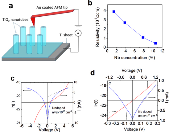
Figure 4. (a) Schematic of the CS-AFM measurements, which allows electrical contact with single hollow nanotubes. This measurement was used to measure electronic properties of individual nanotubes; (b) dependence of resistivity (in 10−3 Ωcm or milliohm. cm) with Nb doping in TCO nanotubes. Current–voltage (I–V) characteristics (red curve) and corresponding ln(I) versus V plots (blue curve), for single undoped (c) undoped nanotubes and (d) Nb doped TiO2 nanotubes (Nb doping level 10.6%).
Download figure:
Standard image High-resolution imageTo further characterize the carrier concentration of the samples, we used CS-AFM I–V in the intermediate bias regime, where the reverse-biased Schottky barrier dominates the total current [30, 31]:
where JS
is the current density through the Schottky barrier, S is the contact area associated with this barrier, E0 is a parameter depending on carrier concentration n, e is electron charge, k is the Boltzmann constant, and Js
is a function of applied bias [30, 31]. The slope of ln(I) versus V is equal to  , where
  , and
, and  , h is the Planck's constant, ε0
is vacuum permittivity, ε = 31 ε0
is the dielectric constant for TiO2, and m* = m0 electron effective mass. This logarithmic plot of the current I as a function of the applied bias V gives approximately a straight line (figure 4(c)), the slope of which is equal to
, h is the Planck's constant, ε0
is vacuum permittivity, ε = 31 ε0
is the dielectric constant for TiO2, and m* = m0 electron effective mass. This logarithmic plot of the current I as a function of the applied bias V gives approximately a straight line (figure 4(c)), the slope of which is equal to  . From the slope, carrier (electron) concentration n can be calculated using expression for E00. The carrier concentration for 1% Nb doped TiO2 sample was 5 × 1019cm-3 (figure 4(d)), which is about two orders of magnitude higher than the electron concentration 9 × 1017 cm−3 in nominally undoped sample (figure 2(c)). The carrier concentration, n, increased with Nb doping and reached 3.4 × 1021 cm−3 for 10.6% Nb concentration in TCO nanotubes. Using the ne
value of ∼3.4 × 1021 cm−3, we estimated that from the doped Nb atoms, ∼90% are electronically active and contribute an additional charge carrier to the electronic states of TCO nanotubes.
. From the slope, carrier (electron) concentration n can be calculated using expression for E00. The carrier concentration for 1% Nb doped TiO2 sample was 5 × 1019cm-3 (figure 4(d)), which is about two orders of magnitude higher than the electron concentration 9 × 1017 cm−3 in nominally undoped sample (figure 2(c)). The carrier concentration, n, increased with Nb doping and reached 3.4 × 1021 cm−3 for 10.6% Nb concentration in TCO nanotubes. Using the ne
value of ∼3.4 × 1021 cm−3, we estimated that from the doped Nb atoms, ∼90% are electronically active and contribute an additional charge carrier to the electronic states of TCO nanotubes.
To understand the high degree of ionization of Nb dopant, we measured the temperature dependent I–V characteristics (I–V–T) of our TCO nanotubes. Using a Richardson plot ln(I/T2) versus 1/kT, we obtained the Nb donor ionization energy (Ea ) as 12 meV (from the high temperature region, figure 5(a)). Similar activation energy (18 meV) was also obtained from the slope of ln(σ) versus 1/kT plot, where σ is conductance I/V (figure 5(b)). This activation energy is very close to reported values of Nb donors in TiO2, which ranges from 4 to 30 meV [12–15]. In order to rule out ionization due to application of bias (or hopping of charges between Nb centers), we also analyzed the activation energy as a function of applied voltage (from Richardson plot, figure 5(c)). The activation energy was found to be constant with applied bias, and hence occurs spontaneously due to available energy at room temperature. Therefore, the low activation energy (obtained from two separate methods [32]) and clear evidence of uniform Nb incorporation (lack of phase segregation or secondary phases) can explain the high degree of incorporation of charge carriers from doped Nb atoms in TCO nanotubes.

Figure 5. (a) Richardson plot ln(I/T2) versus 1/kT, obtained from temperature dependent current–voltage (I–V–T) characteristics for Nb doped TCO nanotubes. Inset shows the high temperature region of the Richardson plot, where thermionic emission was dominant. Using the slope of this region, an activation energy of 12 meV was measured. (b) Conductance (I/V) versus 1/kT for the same nanotubes. The slope gives an activation energy of 18 meV. (c) Activation energy (calculated from Richardson plot) versus applied bias. Constant activation energy with voltage indicates no bias induced ionization or hopping was observed in these nanotubes. These measurements correspond to TiO2 nanotubes Nb doping level of 10.6%.
Download figure:
Standard image High-resolution imageAddition of Nb dopant in TCO nanotubes results in ionization of charge carriers and resulting increase in conductivity (figure 4(b)). To understand the charge transport in these nanotubes, we measured the change in resistivity (ρ = 1/σ) with temperature T (from 20 to 300 K) for an ensemble of TCO nanotubes. The ρ − T data showed two different dependences, pointing to a change in transport behavior. The resistivity of TCO nanotubes with low Nb doping (shown for 1 wt% Nb, figure 6(a)) decreased with temperature, indicating this sample showed typical semiconductor transport. However, for TCO nanotubes with 10 wt% Nb the resistivity monotonically increases with temperature (dρ/dT > 0) showing 'metal-like' behavior (or metallic conductivity). The resistivity for these TCO nanotubes decreased from 6.5 × 10⁻⁴ Ωcm at 300 K to 2.2 × 10⁻⁴ Ωcm at 20 K. This switch from semiconductor to metallic conduction indicates that charge transport in heavily-doped samples is limited mainly by electron–phonon or electron–electron scattering, which decreases at low temperatures leading to a decrease in TCO resistivity [11, 33]. At high temperatures (100–300 K) the ρ − T dependence is almost linear, similar to metals, and can be described by  , where ρ0 is the residual resistivity (∼1.76 × 10⁻⁵ Ωcm), α is the temperature coefficient (1.15 × 10⁻¹ K−1 here), and ΔT is the temperature difference. The carrier concentration n was almost independent of temperature (shows a slight decrease, ∼10%, when the temperature is decreased from 300 K to 20 K, figure 6(b)). Using n, we also extracted the electron mobility μ using the relationship μ = 1/(neρ), where ρ is the resistivity of the TCO nanotubes. For highly doped samples (10 wt% Nb), while the resistivity decreases with temperature, the carrier mobility increases by a factor 3.5 within the same temperature range (from 2.9 to 10.3 cm2 V−1s−1, when temperature changes from 300 K to 20 K, figure 6(b)). This behavior is typical of semiconductor transport, whereas lower conduction electron scattering in heavily-doped TCO nanotubes causes the switch to metallic conductivity (since the charge carrier concentration stays almost the same due to shallow Nb donors, figure 6(b)).

Figure 6. (a) The resistivity of Nb doped TCO nanotubes as a function of temperature, with two different Nb doping levels: 10.6% (curve 1), and 1.3% (curve 2). (b) Carrier concentration (blue) and mobility (green) of 10.6% Nb doped TCO nanotubes, as a function of temperature. Temperature was varied in the range 20–300 K. (c) Transmittance of 10.6% Nb doped TCO nanotubes. Transmittance above 90% was observed in the visible range.
Download figure:
Standard image High-resolution imageBesides the electrical properties, TCO materials are desirable for their light transmission. Optical transparency of metallic Nb doped nanotubes was evaluated using reflectivity measurements. The transmittance η was obtained from reflectance measurements using the following relation:

where Rb is measured signals from blank Ti sheet, Rs is the signal from the sample, and Rd is the background signal. The results, shown in figure 6(c), clearly demonstrate that η is above 90% for most of the visible wavelengths for TCO nanotubes. These results also compare well with ITO thin films which requires conductivities ∼104 Scm−1, while retaining >90% transparency, for TCO applications [2]. While nanotube films in this work were grown on non-transparent opaque Ti sheet, the grown nanotubes can be easily detached from Ti sheet and transferred onto transparent substrates as was shown in previous studies [34–36]. In addition, by deposition of Ti metal on a transparent substrate (e.g. glass) and subsequent anodization of metallic Ti films, completely transparent samples can be obtained [37, 38].
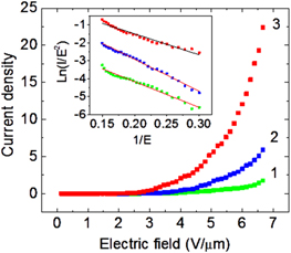
Figure 7. Field emission (IV) characteristics and corresponding Fowler–Nordheim plot (inset) of TCO nanotubes: undoped (curve 1, green), and doped with Nb 1 wt% (curve 2, blue) and 10 wt% (curve 3, red).
Download figure:
Standard image High-resolution image
Due to their high chemical stability and excellent charge conduction properties, we evaluated the field emission properties for these TCO nanotubes. The field emission measurements were performed in a vacuum chamber with a base pressure of 6.6 × 10⁻⁵ Pa, in a voltage range of 0–1000 V. The bias is applied to a copper grid placed at a distance 150 μm from the TCO nanotube surface [39, 40]. We found that Nb doped TCO nanotubes exhibited significantly higher field emission current, compared to undoped samples. Figure 7 compares field emission I–V characteristics of TCO nanotubes doped with 10% Nb (curve 1), 1% Nb (curve 2), and undoped sample (curve 3). The inset shows corresponding Fowler–Nordheim plots for the respective samples. Almost linear behavior of ln(I/E2) versus 1/E shows predominant field emission nature of the emitted electrons. Also, the field emission current increases with Nb doping (22 mA for 10 wt% Nb concentration compared to 1.8 mA for undoped tubes) due to decrease in field emission threshold and increase in electron carrier density. This observation of high field emission current from 10% Nb doped TiO2 nanotubes (22 mA) is unprecedented for oxide nanotubes, and can be improved further by optimization of nanotube density (due to reduction of electric field screening effects) [40].
Recently several groups have tried doping TiO2 nanotubes with Nb [28, 29]. Niobium doping of TiO2 nanotubes using a fluoroniobate complex [28] during the anodization process simultaneously provides a source of the doping element and fluoride anions required for nanotube formation. While the negatively charged fluoroniobate complex allows insertion of Nb in the TiO2 nanotube structure (positive bias), this method requires synthesis of negative charged complexes soluble in the electrolyte. This limits the flexibility of incorporating desired shallow metal dopants, as not every metallic dopant can have negative complex soluble in the electrolyte (usual single atom metal ion precursors are positively charged in electrolyte and repelled from positively biased Ti sheet). In contrast, our method works both with positively and negatively charged ions, and therefore is more easily applicable for formation of different TCO nanotubes. Moreover, while anodizing metallic Ti-Nb alloys [29] allows Nb doped TiO2 nanotubes. the Nb doping was low (up to 0.5 at% N), limited by the Nb portion in Ti–Nb alloy (TCO applications require higher ∼10 wt% doping). Since the alloying method requires special preparation of Ti-metal alloys to grow nanotubes of given dopant concentration, the doping amount is limited by the amount of metal alloy that can be incorporated and requires special preparation of metal–alloy sheets, compared to facile incorporation of dopant metal precursor incorporation demonstrated here.
4. Conclusion
In conclusion, we demonstrate TCO nanotubes by doping TiO2 nanotubes with shallow Nb donors. Nanotubes doped with 10 wt% Nb shows metal-like behavior, with resistivity decreasing from 6.5 × 10⁻⁴ Ωcm at T = 300 K (compared to 6.5 × 10⁻¹ Ωcm for nominally undoped nanotubes) to 2.2 × 10⁻⁴ Ωcm at T = 20 K. Optical properties, studied by reflectance measurements, showed light transmittance up to 90%, within wavelength range 400 nm–1000 nm range. Nb doping also improves the field emission properties of TCO nanotubes (reduction of field emission threshold and increase in emitter current). Therefore, these results can have important consequences for fabrication of porous membranes, made of hollow TCO nanotubes, for a variety of nanostructured photovoltaic, photodetector, photoelectrochemical and photocatalytic devices.
Acknowledgements
This work was supported by start-up funds from University of Colorado, and NSF CAREER Award (CBET-1351281).