
Abstract
We report parallel topographic imaging and nanolithography using heated microcantilever arrays integrated into a commercial atomic force microscope (AFM). The array has five AFM cantilevers, each of which has an internal resistive heater. The temperatures of the cantilever heaters can be monitored and controlled independently and in parallel. We perform parallel AFM imaging of a region of size 550 μm × 90 μm, where the cantilever heat flow signals provide a measure of the nanometer-scale substrate topography. At a cantilever scan speed of 1134 μm s−1, we acquire a 3.1 million-pixel image in 62 s with noise-limited vertical resolution of 0.6 nm and pixels of size 351 nm × 45 nm. At a scan speed of 4030 μm s−1 we acquire a 26.4 million pixel image in 124 s with vertical resolution of 5.4 nm and pixels of size 44 nm × 43 nm. Finally, we demonstrate parallel nanolithography with the cantilever array, including iterations of measure-write-measure nanofabrication, with each cantilever operating independently.
Export citation and abstract BibTeX RIS
1. Introduction
The atomic force microscope (AFM) is widely used for nanometer-scale measurements [1], and is typically used for measuring nanometer-scale surface topography [2]. Arrays of cantilevers can significantly increase measurement area and speed compared to single cantilevers [3]. However, there remains a significant challenge in individually addressing each cantilever, and in operating an array of active cantilevers.
The optical lever setup found in most AFM systems is robust and easy to use, but cannot be easily scaled to large cantilever arrays [4, 5]. Interferometric readout methods enable sensing of individual cantilever deflections with high sensitivity, but such AFM setups require additional optics, processing electronics and specific array geometries to accommodate the laser path [6–8]. Alternatively, cantilever tip height can be sensed by integrating a sensor into each cantilever in the array [3]. Arrays of cantilevers with embedded piezoresistive strain sensors have been used mostly for parallel microscopy and lithography [9–17]. Cantilever arrays with embedded heater-thermometer sensors have a much higher sensitivity than cantilever arrays with integrated piezoresistors [18, 19] and have been used for applications in microscopy, calorimetry and data storage [20–22].
Table 1 summarizes previous publications that have reported cantilever arrays used for parallel imaging and/or lithography. Three important trends can be identified from table 1. First, only a few publications report an array system capable of both imaging and lithography. However we note that a read–write–read capability is necessary for nanomanufacturing [23]. Second, most arrays were integrated into either highly customized commercial AFMs or non-commercial customized AFM systems built specifically for a particular array type. The need for such customized AFMs arises from the complexity of the array technology. Third, complexity in array operation has typically resulted in slow imaging and lithography speeds, low imaging resolution or poor control of lithographic feature size, thereby reducing the throughput advantage of cantilever arrays. A more accessible approach is required in order for cantilever arrays to become more widely used. This paper describes the scalable integration of heated cantilever arrays in a commercial AFM. We demonstrate parallel high speed imaging as well as parallel read–write–read.
Table 1. Summary of studies on parallel imaging and lithography using AFM cantilever arrays. (Note: IM, interferometric sensor; PR, piezoresistive sensor; MH, metal heater-thermometer; SH, doped silicon heater-thermometer; TB, thermal bimorph actuator; PE, piezoelectric actuator; HM, highly modified commercial AFM; CC, completely custom AFM; LM, lightly modified commercial AFM.)
| Investigator | Array size | Sensor | Actuator | AFM | Imaging | Lithography |
|---|---|---|---|---|---|---|
| Shim [51] | 4750 (2D) | — | — | HM | — | 4750 identical copies of pyramid on US $1 bill |
| Wilder [52] | 1 × 2 | — | — | LM | — | Parallel and independent patterning of a photoresist |
| Wouters [53] | 1 × 4 | — | — | HM | — | 4 identical patterns of squares in parallel |
| Bullen [54] | 1 × 10 | — | TB | HM | — | Numbers 0–9 drawn independently |
| Sulchek [55] | 1 × 5 | IM | — | CC | Parallel imaging with 0.09 nm resolution | — |
| Favre [7] | 1 × 4,5 × 7 | IM | — | CC | 35 cantilevers imaged 3T3 cells simultaneously | — |
| Sache [8] | 27 × 27 | IM | — | CC | 9 cantilevers imaged a grating at 21 μm s−1 | — |
| Schneider [12] | 1 × 8 | PR | — | CC | Parallel imaging using 6 probes at 10 μm s−1 | — |
| Aeschimann [10] | 1 × 2 | PR | — | LM | Parallel imaging of a sample in liquid medium | — |
| Sulzbach [11] | 1 × 4,1 × 16,1 × 32,4 × 32 | PR | TB | CC | 8 cantilevers imaged an 1 × 1.36 mm area | — |
| Ivanova [13] | 4 × 32 | PR | TB | CC | 2 cantilevers scanned in intermittent contact | — |
| Chow [14] | 2 × 7 | PR | — | HM | 14 simultaneously acquired scans | — |
| Polesel-Maris [9] | 4 × 4 | PR | — | HM | 16 cantilevers scanned in a liquid medium | — |
| Lange [15] | 1 × 2 | PR | TB | LM | Parallel imaging with 4 nm resolution | — |
| Saya [17] | 1 × 4 | PR | — | CC | 2 cantilevers scanned with 8 nm resolution | — |
| Lutwyche [32] | 5 × 5 | PR | — | CC | Parallel imaging with 22 cantilevers | — |
| Minne [16] | 1 × 10,4 × 8,1 × 50 | PR | PE | HM | 32 cantilevers scanned a 6.4 mm wide grating | 50 identical sets of parallel lines drawn |
| McNamara [20] and Basu [22] | 1 × 8 | MH | — | CC | Parallel imaging with 7.5 nm resolution | Each probe wrote identical pattern of dots |
| Vettiger [3] and Lutwyche [33] | 32 × 32 | SH | — | CC | Parallel imaging with 834 cantilevers | Independent and parallel data storage application |
| Somnath this paper | 1 × 5 | SH | — | LM | Parallel imaging with 5 cantilevers with 0.6 nm vertical resolution or 44 nm horizontal resolution | 5 different patterns drawn and imaged simultaneously |
2. Instrumentation
Figure 1 shows a schematic diagram and scanning electron microscope (SEM) images of the heated cantilever array. The array has five U-shaped cantilevers made of doped single crystal silicon. The design, fabrication and operation of similar microcantilevers has been reported in previous publications [19, 24]. The free end of each cantilever has a 1 μm tall sharp tip with a radius of curvature of 20 nm. The cantilevers have stiffnesses of ∼0.1 N m−1 and resonant frequencies ∼60 kHz. The cantilever temperature was calibrated using the temperature dependence of electrical resistance via Raman microspectroscopy [24, 25].

Figure 1. (a) Schematic diagram and (b) scanning electron microscope (SEM) micrograph of a heated cantilever. The doped silicon cantilever has an integrated resistive heater near the cantilever tip. (c) SEM image of the five-cantilever array.
Download figure:
Standard imageFigure 2 shows integration of the cantilever into the AFM with only two customized components. The array chip was glued to a printed circuit board (PCB) and the cantilever electrical leads on the chip were wire-bonded to the corresponding pads on the PCB. The PCB was secured onto a customized AFM holder that could be mounted in the AFM. A flex cable connected the PCB to a circuit board containing the cantilever temperature control circuits.

Figure 2. Array integration hardware. The array was glued, then wire-bonded to a printed circuit board (PCB) having electrical leads leading to a flex-cable connector. The PCB was secured onto a customized AFM holder which was mounted in the AFM.
Download figure:
Standard imageFigure 3 shows the schematic for the cantilever array heating control [26]. The control circuit for each cantilever consisted of the heated cantilever, RC, in series with a current-limiting sense resistor, RS. A Labview program translated the resistance set-point,  , of each cantilever to a gain voltage
  . Data acquisition boards (DAQ), National Instruments PXI 6368 and PXI 6733 applied VG to an analog multiplier chip, Analog Devices AD633. The multiplier chip applied the product of VG and the voltage across RS,VS to the heating circuit, thus completing a feedback loop to control cantilever resistance. Low-pass filters (LPF) with cut-off frequencies at 13 and 30 kHz filtered the VG and VS signals. The DAQ simultaneously acquired VS from all cantilevers to enable measurement of thermal topography and to monitor cantilever heating in real time. The DAQ also acquired trigger signals from the AFM controller to aid parallel lithography and imaging, which are described later.
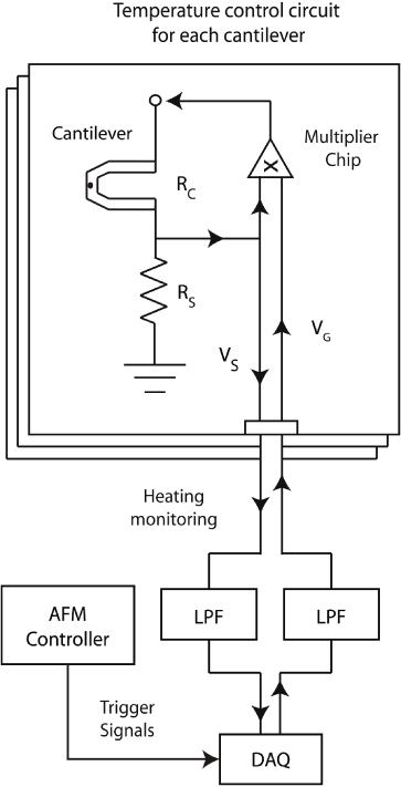
Figure 3. Schematic diagram of the cantilever array heating control. The temperature of each cantilever was held constant using a feedback loop implemented in analog circuitry. A data acquisition board monitored the cantilever heating and acquired the thermal signals from the cantilever.
Download figure:
Standard image3. Application to topographic imaging
Figure 4 shows the concept of thermal topographic imaging with a heated cantilever. Most of the heat generated in the cantilever heater region flows into the substrate via conduction through the air [27, 28]. The thermal conductance of the cantilever is inversely proportional to the distance between the cantilever and the substrate. The power required to maintain a constant cantilever temperature varies with the distance between the cantilever and the substrate, and so the topography of the substrate can be measured by monitoring changes in the cantilever power or voltage as the cantilever scans the substrate.
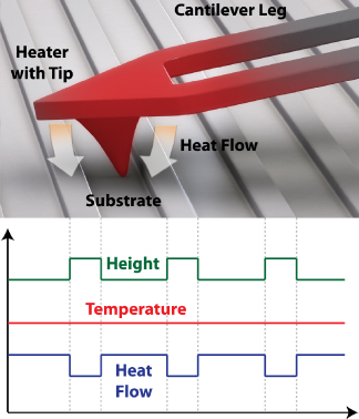
Figure 4. Working principle for thermal topographic sensing. Thermal conductance from the cantilever depends inversely on the cantilever-substrate distance. The topography of the substrate is mapped by tracking changes in the cantilever power dissipation while the cantilever temperature is held constant.
Download figure:
Standard imageFigure 5(a) shows the cantilever voltage and the tip force as the cantilever base is moved toward and retracted from the surface [29, 30]. In step A, as the cantilever approaches the substrate from a distance, the tip force remains zero while the cantilever voltage rises rapidly due to the relation between cantilever heat flow and the cantilever-substrate separation. In step B, the cantilever snaps into contact with the substrate due to an attractive force between the tip and the substrate, which results in a decrease in the cantilever force and a small increase in the cantilever voltage. In step C, the cantilever bends as its base moves, causing an increase in tip force. The cantilever voltage rises gradually since the distance between the heater and the substrate remains unchanged and only the legs bend toward the substrate. When the cantilever base is retracted from the surface, the voltage and force curves retrace their paths, except in section D when the cantilever snaps off from the substrate. When the cantilever is away from the surface, most of the heat flows along the cantilever's legs into the chip holding the cantilever. As the cantilever approaches the substrate surface, heat flows from the cantilever heater, through the air and into the substrate. The shape of the curves in figure 5 indicates the transition from heat conduction along the cantilever to heat conduction through the air and into the substrate [30, 31].
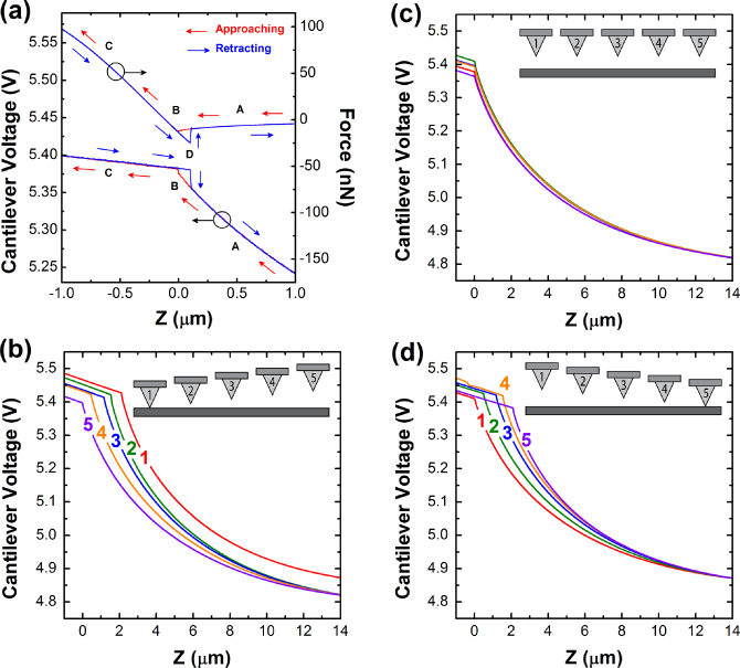
Figure 5. Leveling cantilever arrays onto the substrate using the thermal signals from the cantilever. (a) Cantilever voltage and tip force obtained in a force–displacement experiment. In section A the cantilever heat flow and voltage rise rapidly until the cantilever contacts the substrate. In section C the heat flow increases while the cantilever bends away from the substrate. The direction and extent of array misalignment is measured using the distances at which the cantilevers touch the surface. The array tilt is adjusted until all cantilevers contact the substrate simultaneously. (b) Cantilevers touch the substrate in ascending order. (c) All cantilevers in the array contact the substrate at the same time. (d) Cantilevers touch the substrate in descending order.
Download figure:
Standard imageHeated cantilever arrays were leveled onto a substrate by tracking the position at which the tips snap into the substrate in the cantilever voltage signals. The tilt of the AFM head was adjusted until all the cantilevers in the array engaged simultaneously. Figures 5(b)–(d) show the cantilever voltage in misaligned and well aligned arrays brought into contact with the surface. The same technique can be used to level a two-dimensional cantilever array onto a substrate—one alignment routine along a row and another along a column of cantilevers. After this leveling procedure, the plane containing the array is parallel to the substrate and all cantilevers apply approximately the same vertical force onto the substrate. Vertical position feedback on any one cantilever ensures that the array is always translated in a plane parallel to the substrate. Since this alignment technique obviates the need for optical access to each cantilever, this technique can be automated and scaled to very large cantilever arrays [32, 33].
To demonstrate parallel topography imaging, the array scanned a 550 μm × 90 μm area of a substrate having silicon oxide nanostructures patterned onto its surface. The sample contained the text 'ILLINOIS' patterned as 25 nm tall nanostructures and the text 'UIUC' patterned as 100 nm tall structures within the former pattern. The lateral sizes of the pattern ranged from 1.1 to 53 μm.
The tip-to-tip distance between cantilevers in the array (110 μm) is larger than the maximum scan size (90 μm) of the AFM scanner. In order to image the whole surface, each of the cantilevers in the array each scanned three adjacent sections 45 μm × 90 μm in area. The AFM stage motor moved the sample by 37 μm in the slow-scan direction between scans. The 15 thermal topography images were stitched together to make the complete topographic image for each imaging experiment. Thus the total area scanned by each cantilever was 110 μm × 90 μm and the total area scanned by the array was 550 μm × 90 μm.
Table 2 lists the experimental parameters used for two separate parallel imaging experiments. Experiment A focused on high vertical resolution (figure 6), while experiment B maximized lateral resolution (figure 7). Each cantilever in the array scanned the substrate at 1.13–4.03 mm s−1 in contact-mode AFM simultaneously while the cantilever temperature set-point was ∼500 °C. Since the temperature control circuits autonomously maintained cantilever temperature with 1 MHz bandwidth, the DAQ was free to simultaneously acquire VS from all cantilevers as the thermal topography signal at 1–2 MHz. The cantilever signal was filtered through the analog low-pass filter followed by a software routine that averages 20–80 raw data samples to make one topographic pixel.
Table 2. Operating modes for parallel imaging experiments.
| Parameters | Experiment | |
|---|---|---|
| A | B | |
| 1 scan with each cantilever: | ||
| Scan dimension (μm × μm) | 45 × 90 | 45 × 90 |
| Scan area (μm2) | 4050 | 4050 |
| Scan lines | 128 | 1024 |
| Scan points | 1984 | 2112 |
| Pixel size (nm × nm) | 351 × 45 | 44 × 43 |
| Scan speed (mm s−1) | 1.13 | 4.03 |
| Sampling rate (MHz) | 1 | 2 |
| Averaged samples per pixel | 80 | 20 |
| Complete scan with array: | ||
| Scan dimension (μm × μm) | 550 × 90 | 550 × 90 |
| Scan area (μm2) | 60 750 | 60 750 |
| Pixels | 1565 × 1984 | 12 515 × 2112 |
| Pixels (in millions) | 3.1 | 26.4 |
| Scan duration (s): | 62 | 125 |
| Vertical resolution (nm): | 0.6 | 5.4 |
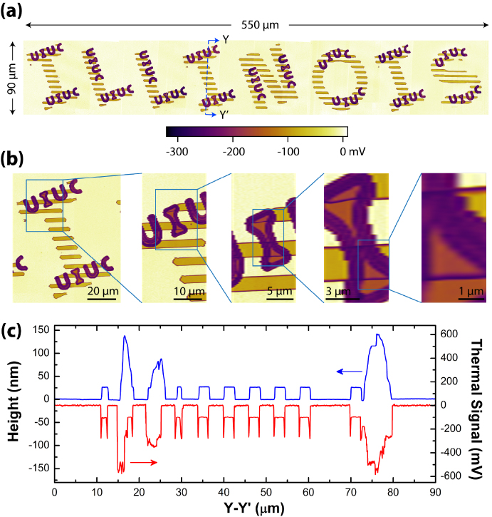
Figure 6. (a) A 550 μm × 90 μm composite AFM image consisting of 3.1 million pixels, acquired simultaneously with five cantilevers. The array scanned the sample in contact-mode AFM at 1.13 mm s−1 and the image was acquired in 62 s. Each cantilever scanned three adjacent rectangular areas and the resulting 15 scans were stitched together to make the complete image. The noise-limited vertical resolution is 0.6 nm. (b) Successive topographic images. (c) Height and corresponding thermal topography line-scans from a single scan showing high vertical resolution in the thermal topography signal. This image corresponds to experiment A from table 2.
Download figure:
Standard image
Figure 7. (a) A 550 μm × 90 μm composite AFM image consisting of 26.4 million pixels, acquired simultaneously with five cantilevers. The array scanned the sample in contact-mode AFM at 4.0 mm s−1 and the image was acquired in 125 s. Each cantilever scanned three adjacent rectangular areas and the resulting 15 scans were stitched together to make the complete image. The noise-limited vertical resolution is 5.4 nm but the pixels are 43 nm × 44 nm. (b) Successive topographic images showing the high lateral resolution. (c) Height and thermal topography line-scans from a single scan. This image corresponds to experiment B from table 2.
Download figure:
Standard imageFigure 6 shows a 550 μm × 90 μm AFM image of the substrate acquired simultaneously using five cantilevers from experiment A. The image consists of 1565 × 1984 pixels of size 351 nm × 45 nm. This image contains 3.1 million pixels and was acquired in 62 s. The topographic signals from all cantilevers show an inverted topography of the sample due to the inverse relation between the cantilever power dissipation and the cantilever-substrate separation distance. The topographic images in figure 6 show artifacts at the edge of vertical features typical of thermal topographic signals [27] since the images were obtained from the raw, unfiltered data. Thermal topographic sensitivity is the change in the cantilever voltage per unit change in the substrate topography while the noise-limited imaging resolution is the smallest vertical displacement that can be resolved by the thermal signal of the cantilever. The line-scans in figure 6(b) show that the topographic sensitivity is about 3.0 mV nm−1 and the noise-limited vertical resolution is 0.6 nm. The measured vertical resolution is an order of magnitude higher than in previous work [34].
Figure 7 shows the results of experiment B, which is a 550 μm × 90 μm AFM image of the substrate acquired simultaneously using the five-cantilever array. The image consists of 12 515 × 2112 pixels that are 43 nm × 44 nm. The 26.4 million pixel image was acquired in 125 s. Some topographic features in figure 7 are skewed and shrunken in size due to the degradation of the closed-loop scanning motion of the sample stage at high scan rates. For experiment B, the vertical resolution is 5.4 nm since fewer samples are available for down-sampling owing to the limited sampling rate of the DAQ.
4. Application to nanolithography
We demonstrate the controlled nanofabrication capability of heated cantilever arrays via repeated sensing, fabrication and repair of nanostructures through alternating steps of parallel thermomechanical lithography and thermal topographic imaging. In thermomechanical lithography, a moving cantilever draws trenches into a substrate via normal load and by heating the cantilever above the reflow temperature, TR, of the substrate [3, 35, 36]. Due to the sharpness of the tip, the thermal resistance between the tip and substrate and the thermal spreading resistance within the substrate dominate the heat flow from the tip to the substrate. Thus, the tip–substrate interface temperature is lower than the heater temperature and can be estimated through finite element simulations or by using an electro-thermal cantilever [37, 38]. Substrate topography in the thermal signal can be resolved beyond heater temperatures of ∼125 °C and the resolution improves with increasing heater temperature. We chose a fluorocarbon thin film, deposited in a reactive ion etching chamber using CF4, as the film for lithography because its high TR of 350 °C provides a large window for thermal imaging of the substrate without erasing the lithographic patterns. The substrate was an 80 nm thick fluorocarbon film deposited on a silicon dioxide sample having 3 μm wide and 20 nm deep cylindrical pits. All cantilevers thermally imaged the substrate simultaneously at 65 μm s−1. Optical tip force feedback was used on one cantilever only to compensate for the out-of-plane misalignment in the substrate rather than tracking the topography of the substrate by setting the integral gain of the cantilever height feedback to 0.5. Each cantilever was programmed to fabricate two unique and complementary patterns for two steps of lithography. For each cantilever, the coordinates of the lithographic patterns were aligned to the circular patterns on the substrate using the aforementioned topographic images. During lithography, all cantilevers moved together at 0.5 μm s−1; however, each cantilever drew a unique pattern since it was heated only when the coordinates of the tip coincided with that of the programmed lithographic pattern. At all other times, the cantilever temperatures were maintained well below the TR of the fluorocarbon to prevent the cantilevers from writing. The array performed two sets of write–read following the initial read step. In the second write step, the cantilevers used lower lithographic temperatures to produce thinner and shallower features when compared to the first lithography step.
Figure 8 shows parallel thermal topography images before and after two steps of parallel thermomechanical writing. The figure shows that at each lithographic step, each cantilever fabricated unique nanostructures that interfaced well with the cylindrical pits on the substrate as well as previously fabricated nanostructures. Figure 9 shows the topographic images and line-scans for cantilever 1 after the first and second lithographic steps. The cantilever voltage signal was multiplied by the topographic sensitivity to obtain the line-scan topography in nanometers. The patterns written in the first lithographic step are about 60 nm deep and 159 nm wide while the patterns written in the second lithographic step are 21 nm deep and 126 nm wide.

Figure 8. (a) Topographic images of a substrate before and after two steps of parallel thermomechanical nanolithography. First, the array thermally imaged the substrate. Unique nanolithographic patterns were registered with and written on top of existing cylindrical pits on the substrate. The cantilevers performed parallel nanolithography and then parallel nanoimaging. Next, the cantilevers wrote patterns that were registered with the previous write step. This second nanolithographic step was at a lower writing temperature to create shallow, narrow features. Finally, the array imaged the substrate again.
Download figure:
Standard image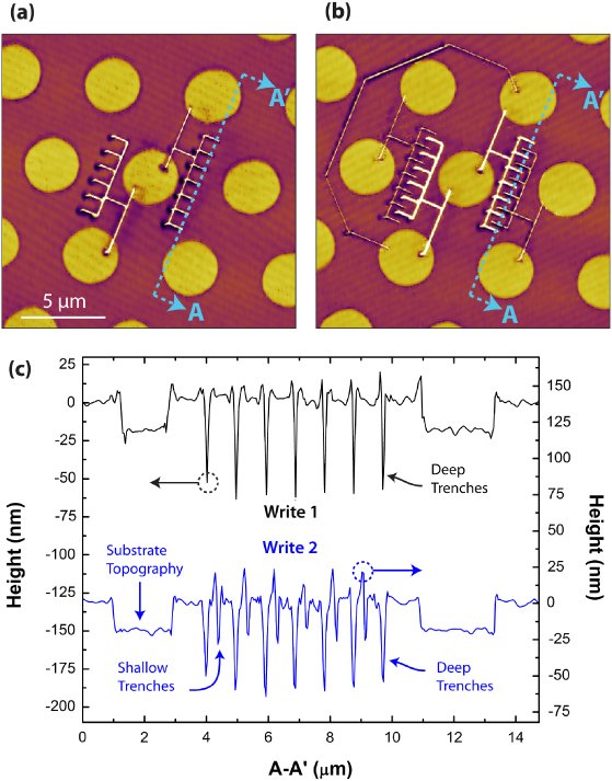
Figure 9. Substrate topography after two parallel steps of thermomechanical lithography. Thermal topographic images of the substrate acquired by cantilever 1 after (a) the first and (b) the second lithographic steps. (c) Line-scans of substrate topography after the (top) first and (bottom) second write steps. Deep trenches were written in the first step and shallow trenches were written in the second step.
Download figure:
Standard image5. Discussion
We made several component and system design considerations to achieve high performance from the array integrated into our AFM system. Misalignment in the array can lead to excessive tip forces or poor substrate contact for cantilevers. It is important to maintain a relatively low and uniform tip–substrate force for all cantilever tips, in order to avoid tip and sample damage. Independent actuators for each cantilever would alleviate this problem; however, there are challenges to scaling this approach [39]. Therefore, we integrated the arrays into an Asylum Research MFP-3D AFM, since the MFP-3D head provides pitch and roll alignment for conformal leveling of the array onto the sample. Uneven forces resulting from the minor remaining misalignment are minimized due to the high cantilever compliance [24]. Because of our approach to the control of height position, the resulting tip–substrate force precludes some applications such as imaging biological samples or delicate polymers where force control is critical. However, there are other applications in which force control is important but not critical, and for which the current approach is sufficient. Examples of such applications include data storage, imaging, lithography and calorimetry on hard surfaces [3, 27, 40, 41]. Closed-loop feedback implemented in the X–Y scanner limited the system drift to about 20 nm between the two lithographic steps in section 4. This drift is common for a scan with a duration of several minutes, even when operating only a single cantilever.
Commercial AFMs are not equipped with software or hardware to enable parallel and independent operation of cantilevers in an array. Another advantage of using the Asylum Research AFM is that the software can be edited, which allowed seamless integration of array-specific software with the existing AFM software. Furthermore, the onboard DAQ in the AFM was reprogrammed to communicate lithographic and imaging trigger information with our National Instruments DAQ that controlled the cantilevers.
The analog cantilever temperature control circuit architecture provides three key benefits. First, cantilever temperatures are maintained within an accuracy of 1.73 °C and precision of 0.076 °C at 1 MHz and are not susceptible to drift due to the closed-loop nature of the feedback [26]. Second, closed-loop control of cantilever temperature enhances thermal topographic sensitivity [34] and consistency in thermal lithography [42]. Third, since the analog circuits work autonomously while being simple, robust and inexpensive, this architecture can be scaled to very large cantilever arrays while maintaining a bandwidth of 1 MHz per cantilever. Implementing such parallel temperature control in the software would result in a very slow cantilever thermal response rate due to the inverse relationship between the array size and the software temperature control bandwidth per cantilever [34].
In addition to the topographic sensitivity and the resolution, the thermal imaging performance can be further characterized by the imaging speed, lateral resolution and imaging area. These imaging parameters are interdependent and are currently limited by the experimental equipment rather than fundamental properties of the cantilever. The best lateral resolution is fundamentally limited by the tip radius (in this case 20 nm), and the best vertical resolution is fundamentally limited by the electronic noise of the cantilever. However, the lateral resolution, vertical resolution and imaging speed are limited by trade-offs between each other due to the fixed data sampling rate and the noise in the thermal signal of the cantilever. The fixed sampling rate results in a compromise between the number of pixels per unit time (quotient of imaging speed and lateral resolution) and the noise per pixel (which affects vertical resolution). The noise was dominated by the electronics (10 mV at 2 MHz bandwidth) rather than the noise floor of the cantilever (2 μV Hz−1/2) [43]. The noise remaining in the filtered signal was inversely proportional to the number of raw data samples available for averaging; thus, the sampling rate limits the noise. For example, imaging experiment A has good vertical resolution at the cost of lateral resolution and imaging speed while experiment B maximizes lateral resolution and imaging speed at the cost of vertical resolution. The results of this paper show an improvement of about 10 times over our previous work, which used a different electronic interface [34].
The imaging speed of our system is currently limited by the X–Y scanner and is approaching the limits of the thermal time constant of the cantilever (10 μs) and the mechanical time constant (16 μs) [24]. When imaging with a pixel width of 44 nm, the thermal time constant of the cantilever limits the imaging speed to 4.5 mm s−1 and the mechanical time constant limits the imaging speed to 2.8 mm s−1. However, figure 7 shows that even though imaging speed was greater than 2.8 mm s−1, the vertical features of the 25 nm structures are only slightly tilted. This is because the cantilever can begin to respond to small thermal or mechanical changes more quickly than the time constants. Furthermore, the topographic sensitivity is the same at 4.03 mm s−1,1.13 mm s−1, and also at slower imaging speeds [26]. The fundamental limit on imaging speed could be raised by altering the cantilever geometry to reduce the mechanical and thermal time constants.
Heated cantilevers can be operated over a large temperature range, up to 1000 °C, which enables several applications in metrology and manufacturing [24, 44]. We chose to perform tip-based nanofabrication using thermomechanical lithography on the fluorocarbon film due to the simplicity of the lithographic technique and the ease of reading and writing the nanostructures. However, the same array integration architecture can also be used to fabricate nanostructures via thermochemical nanolithography (TCNL) [45, 46] and thermal dip pen nanolithography (tDPN) [40, 47]. It is possible to fabricate nanostructures smaller than the tip diameter with the appropriate choice of the thermal lithographic technique and lithographic substrate [46, 48]. The speed of lithography can range from 100 nm s−1 to more than 1000 μm s−1 depending on the application [46]. Large heated cantilever arrays can potentially be used to create multi-material three-dimensional nanometer-scale devices via tDPN or graphene electronic devices via TCNL [49]. Other applications of this integrated array of heated AFM cantilevers in includes local thermal analysis (LTA) [41, 50] and data storage [3].
6. Conclusions
In summary, we demonstrate scalable integration of heated cantilever arrays in a commercial AFM to perform parallel nanolithography and nanometer-scale topographic imaging. Cantilever temperatures are controlled independently via closed-loop feedback implemented in analog circuitry. The array is aligned onto the substrate by tracking changes in cantilever power instead of using the traditional laser–photodetector setup. The array performed parallel imaging of a 550 μm × 90 μm area at 1.1 mm s−1 with 0.6 nm vertical resolution and at 4.0 mm s−1 with 44 nm lateral resolution. The array performed multiple iterations of parallel thermomechanical lithography and thermal topographic imaging to fabricate and measure nanometer-scale structures.
Acknowledgments
This work was supported by the NSF Center for Chemical–Electrical–Mechanical Manufacturing Systems, NSF CMMI 10-68723, and DARPA TBN.