
Abstract
The early stages of electroforming in TiO2 were explored using a combination of electrochemical strain microscopy and local I–V curve measurements. Negative differential resistance and corresponding surface deformation were observed below the electroforming voltages. Electrochemical strain microscopy allowed probing of the changes in local electrochemical activity during the pre-forming and forming stages. The associated structural changes were visualized by transmission electron microscopy. The results allowed an understanding of the electrochemical processes in the early stages of electroforming, and provide a comprehensive approach for exploring irreversible and partially reversible bias-induced transformations in solids.
Export citation and abstract BibTeX RIS
1. Introduction
Electroresistive switching in metal oxides has been actively explored for several decades, with the earliest example of metal–metal oxide coherer dating back over 100 yr [1]. The explosive resurgence of this field in the last few years is due to the newly realized potential of electroresistive systems for high-density memory applications, as well as memristive properties as suggested by the HP group [2, 3]. Non-volatile memories based on electroresistive materials have attracted broad interest due to a combination of low writing energy, simple device architecture, and easy scaling down to atomic limits [4–6]. The presence of multiple resistive states can be further explored to enable multilevel memories and neuromorphic logics [7–9]. Coupling between ionic and magnetic degrees of freedom gives rise to applications in semiconductor spintronics and adaptive filters [10, 11]. Recently, interest in ionically mediated phenomena in transition-metal oxide systems has arisen in the context of ferroelectric tunneling barriers, in which significant changes in the interface chemistry are observed with high-resolution scanning transmission electron microscopy [12], refining original models based on purely physical mechanisms [13–17]. Finally, it is of interest to explore new functionalities in memristors, taking advantage of recent progress in oxide electronic and optoelectronics devices, e.g. negative differential resistance (NDR), light emission, etc, which will enable novel applications [18–20].
A critical issue for memory applications is an understanding of operational mechanisms such as electroforming, including thermal and electrochemical effects, and subsequent resistive switching in the formed filamentary system [21–25]. In TiO2 memristive materials, the forming and switching mechanisms are controlled by the interplay of ionic transport, the interfacial electrochemical process, and the formation of vacancy-ordered second phases assisted by local thermal effects [21–26]. When bias voltage is applied to the sample, oxygen vacancies are formed and subsequently order, ultimately resulting in phase change from a nonconductive fully-oxidized phase to a conductive oxygen-deficient Magnéli phase. Recently, the post-formation structure of conductive filaments was studied in detail using a combination of focused ion beam sectioning and diffraction pattern analysis in transmission electron microscopy (TEM) [26]. Both the reversible and irreversible stages of memristor formation and operation depend on the microstructure and defects that serve as nucleation centers and pinning centers, etc. Hence, of particular interest for device operation are phenomena preceding the formation of a conductive filament, including generation of oxygen vacancies, early stages of decomposition of the non-stoichiometric TiO2, and precipitation of Magnéli phase nuclei. Without this understanding, formation of the conductive filament remains an essentially uncontrollable stochastic process, limiting the scalability of the device and the reproducibility of the switching.
The strong first-order character of the electrochemical processes in memristors and the significant role of defects necessitate local studies of the formation and operation using localized electrodes. To date, the technique of choice has been conductive atomic force microscopy (CAFM), commonly used to probe conductive current behavior, which is indirectly linked to redox behavior (unlike detection of Faradaic currents that provide direct information on electrochemical process). However, CAFM studies of memristive behavior are limited by the irreversibility of the process, precluding mapping on dense grids similarly to, e.g., polarization switching [27, 28]. In addition, a rapid change of CAFM signal is associated with filament formation, therefore it is rather difficult to access to the early stages of electroforming. In comparison, electrochemical strain microscopy (ESM) allows exploration of the electrochemical process at a nanoscale in the absence of conductive currents [29–31]. Here, we combine CAFM and ESM to study the local electrochemical behavior at the early stages of electroforming in TiO2 memristive materials.
2. Materials and methods
2.1. Fabrication of TiO2 films
25 and 30 nm thick TiO2 thin films were prepared on Pt/TiO2/Si substrates by atomic layer deposition (ALD) at a growth temperature of 150 °C. Titanium (IV) tetraisopropoxide (TTIP; Ti[OCH(CH3)2]4, 99.99%) and deionized water vapor were used as a Ti precursor and an oxidant, respectively. The two precursors were contained in separate stainless steel canisters, which were heated to 40 °C for the TTIP and maintained at room temperature for the water. TTIP vapor was delivered to the process chamber with a pure N2 gas (99.999%) at a flow rate of 100 sccm. The unit ALD cycle was composed of TTIP exposure (3 s), N2 purge (10 s), water vapor exposure (0.2 s), and N2 purge (10 s). N2 gas at a flow rate of 200 sccm was injected into the process chamber during the N2 purge. According to x-ray diffraction analysis, the resulting TiO2 film turned out to be amorphous.
2.2. CAFM and ESM measurements
Scanning probe microscopy studies were performed on a commercial system (Asylum Research Cypher) equipped with a current amplifier (Femto DLPCA-200) and home-built Labview/Matlab. A glove box (MBraun) filled with Ar was used for environmental control. During the voltage–current measurements, series resistors of 10 or 30 MΩ were used to limit maximum current levels. ESM measurements were carried out using a band-excitation (BE) waveform of 80 kHz width centered on the contact resonance (315 kHz) and an amplitude of 1.5Vpp applied to a Pt/Cr coated probe (Budget sensors ElectriMulti75-G). The BEPS–ESM measurements were performed in a voltage range of ±6 V and collected the hysteresis loop in the off-field mode over an area of 10 × 10 μm2. Smoothing was performed for each topographic difference image. Notably, it has been commonly accepted that the surface adsorbates can affect the absolute value of the measured signal, without significantly affecting the comparative measurements along the surface [32, 33]. In addition, capacitance is present and is in parallel to the resistance/capacitance of the tip–surface junction. Since the signal in electromechanical based AFMs such as ESM is affected by the potential induced by the tip at the tip–surface junction, the signal for sufficiently high input impedance of the current source is unaffected by the cantilever–surface capacitance and other non-local elements of the equivalent circuit [34]. Hence, the cantilever–surface capacitance does not affect the ESM signals.
2.3. TEM measurements
TEM studies were performed on an FEI Titan aberration-corrected TEM. A TEM sample was prepared by a Hitachi NB5000 dual-beam instrument with one electron beam column and one ion beam column, focused at the region deformed by positive bias sweep up to +7 V in 25 nm TiO2 thin films.
3. Results and discussion
3.1. Negative differential resistance and the corresponding surface deformation
Here, we explore the variability of memristive formation using multiple I–V measurements over a spatial grid of 10 × 10 points over an area of 16 × 16 μm2. In order to avoid hard dielectric breakdown, the measurement circuit included current limiting series resistors of 10 or 30 MΩ. At each grid point, two different positive voltage sweeps were applied to a conductive probe. The first (forming) bias sweep induced an electrochemical process under a high electric field, and the second (probing) bias sweep was used to establish whether its electrical state was changed.
Figure 1 shows I–V curves and their corresponding topographic difference images. For I–V measurements, voltages were applied up to 12 and 20 V, respectively. Interestingly, all the I–V curves show NDR features at around 7–8 V (see the blue arrows in figures 1(a) and (c)). In the inset of figure 1(a), a histogram of maximum voltages of the NDR feature (VNDR) shows a very uniform distribution at around 7.5 V. After the I–V measurements of figures 1(a) and (c), a uniform surface deformation (disk shaped feature on the topographic image) is observed at each measurement location, as shown in figures 1(b) and (d). The magnitude of surface deformation was about 0.3–0.4 nm. The lateral size of the disks in figure 1(d) was broader than those in figure 1(b). Note that the large size (>600 nm) as compared to the 10–30 nm tip–surface contact area indicates a large column of bias-transformed region and can be related to the water layer on the sample surface. These surface deformations could be observed after >10 h, indicative of thermodynamic stability.

Figure 1. (a), (c) Representative I–V curves with (a) 10 and (c) 30 MΩ. (b), (d) Topographic difference images before and after the I–V measurements of (a) and (c) in 30 nm-thick TiO2 thin films. The blue arrows show the current bump which indicates the starting point of NDR. Smoothing was carried out for the topographic difference images. The inset shows a histogram of maximum voltages of the NDR feature (VNDR). The scale bar is 3 μm.
Download figure:
Standard imageUnder a positive bias to the top electrode, an oxygen gas bubble can be generated at the interface between the top electrode and the memristive material [35]. However, in this case the top electrode is absent and hence bubble formation in the near-surface layer is unlikely. Furthermore, complete electroforming was not achieved by the first bias sweep (see the second bias sweep in figures 1(a) and (c)). Even though the TEM data indicate partial crystallization of the material (see figure 6(b)), this process decreases the molar volume and hence cannot account for the observed behavior [36]. Thus, a gas bubble and complete electroforming can be excluded as possible reasons for the NDR behavior and corresponding surface deformations. As an alternative mechanism, oxygen species such as O2,O−, or O2− can be adsorbed on the sample surface under high applied bias voltage. The attractive force by the adsorbed oxygen species can contribute significantly to the topographic imaging by non-contact mode AFM [37]. However, accumulation of adsorbed oxygen is hardly detectable by contact mode AFM. Furthermore, similar topographic change was observed even using a much stiffer cantilever (diamond coated cantilever, >40 times higher than a Pt/Cr coated cantilever) under a higher contact force (not shown here). Since there is a clear long-lasting topographic change, the adsorbed oxygen can be excluded as a dominant phenomenon in the topographic change.
Finally, the surface deformation may be related to the defect states of the present TiO2 thin films. Since Ti interstitials can exist on TiO2 surfaces and, furthermore, can be oxidized [38, 39], surface deformations can occur under positive bias sweeps due to the field-enhanced surface oxidation [40, 41]. In other words, non-stoichiometric TiO2 transforms to the stoichiometric insulating state, resulting in the NDR effect. To confirm the field-enhanced surface oxidation as a possible reason for the surface deformation, the same experiments as shown in figure 1 were performed using the AFM enclosed in a glove box filled with Ar (O2 and H2O partial pressures below the 1 ppm level). During the positive bias sweeps, there was no distinguishable current bump in the I–V curves (see figure 2(a)). This indicates that there is no NDR behavior under an Ar atmosphere. Furthermore, surface deformations were not observed after the positive bias sweeps. The I–V curves and corresponding topographic information clearly confirmed that oxygen is a required component in the observed phenomena, and hence the field-induced surface oxidation is responsible for the formation of the surface deformation.

Figure 2. (a) Representative I–V curves with 10 MΩ measured in a glove box filled with Ar. (b) Topographic difference images before and after the I–V measurements in 30 nm-thick TiO2 thin films. Smoothing was carried out for the topographic difference images. The scale bar is 3 μm.
Download figure:
Standard image3.2. Reversibility of the surface deformation
We further explored the reversibility of the electrochemical processes that yield static surface deformations though different polarity sequences of bias sweeps. First, positive and subsequent negative bias sweeps (A bias sweep in figure 3(a)) were carried out at four different locations. As a reference point, single positive bias sweeps, which were similar to those in figure 1, were carried out at the center of the scanned region (B bias sweep in figure 3(a)). The I–V curves of both figures 1(b) and (c) show the NDR phenomena in the positive bias sections. However, only the B bias sweep shows surface deformation and there is no surface deformation after A bias sweeps, as seen in figure 3(d). This means that a negative bias sweep just after a positive bias sweep leads to recovery of surface deformation. Hence, the formation of topographic protrusions and NDR are the result of local surface oxidation that can be reversed by local reduction. This scenario is further confirmed by the large fluctuations in current during the negative bias sweep, indicative of an electrochemical process near the surface and tip–surface contact instability. Thus, it was found that the static surface deformations can be reversed by applying different polarity of the bias sweeps.

Figure 3. (a) Schematic of I–V measured locations. (b) Representative positive and subsequent negative and (c) positive bias sweeps at A and B in (a). (d) Topographic difference images before and after the I–V measurements. Smoothing was carried out for the topographic difference images. The scale bar is 3 μm.
Download figure:
Standard image3.3. Electrochemical activity of the surface deformed region
The CAFM results in figures 1 and 3 show the NDR and the corresponding surface deformation. However, CAFM measurements are limited by the fact that the measurements are non-local, i.e. the conductivity of the whole material region between the tip and the bottom electrode is probed. Furthermore, the relationship between oxygen vacancy concentration in TiO2 and conductivity is highly complex [42], precluding an unambiguous picture of oxygen vacancy dynamics in the near-surface layer from being obtained. To complement CAFM studies, we probed the near-surface oxygen vacancy behavior using ESM. ESM was originally developed for Li-ion conductive materials [29, 43, 44] and recently applied for oxygen ion conductors [31, 45]. ESM probes electrochemical activity including oxygen reduction and evolution (redox) processes using bias-induced electrochemical strain as the measured signal [29, 31]. Here, we explore the electrochemical activity on the pristine and electroformed TiO2 surfaces through spatially resolved ESM hysteresis loop measurements.
Figure 4(a) shows disk-type surface deformations formed by the same bias sweeps as figure 3(c) at four different locations. As shown in the inset of figure 1(a), surface deformations occur at voltages higher than 6.5 V. Therefore, in order to explore the electrochemical behavior without further surface deformations, ESM measurements were carried out in the bias range of ±6 V, i.e. below VNDR. In this manner, we both characterized the reversible electrochemical transformations under the tip and ascertained the changes in the reversible electrochemical activity due to the irreversible surface changes induced by prior application of bias pulses. We further monitored current behavior during ESM to correlate the changes in local conductivity and electrochemical activity.
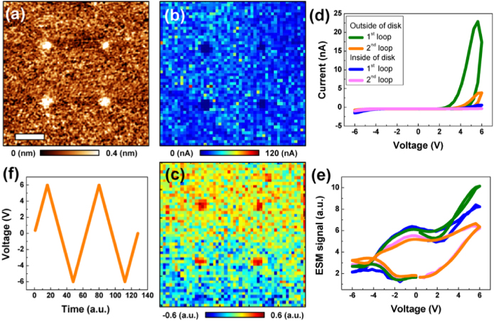
Figure 4. (a) Topographic difference image after I–V measurements using the same bias sweep of B in figure 3 at four different places. (b) Maximum current map and (c) mathematically analyzed ESM image of first loop. (f) Bias voltage sweep and corresponding (d) average I–V and (e) ESM loops at the inside and outside of the disks. The smoothing was done for topographic difference images. Scale bar is 2 μm.
Download figure:
Standard imageThe four disks formed by the application of anodic waveforms clearly show lower maximum current compared to the outside of the disks, as is visible in the maximum current map of the first loop of figure 4(b). This is also visible in the average I–V loops of figure 4(d) and the maximum current map of the second loop (not shown here). Interestingly, the second I–V loop on the outside of the disks shows a much lower current level compared to the first one. The insides of the disks also show the same behavior, but the absolute values are much lower. This indicates that, even though there is no surface deformation under ±6 V, there can be electrochemical processes that are relevant to the electrical properties, e.g. crystallization and/or the early stages of redox processes, etc.
Changes in the electrochemical activity were also observed in the ESM loops in the bias range of ±6 V (see figure 4(d)). The clear loop opening in the ESM loops shows that there are electrochemical processes during the bias sweeps. Since the increase of the ESM signal occurs earlier than that of the current signal (see figures 4(d) and (e)), it indicates that electrochemical reactions occur at lower bias voltages before current flows. Indeed, the operational principle of ESM is based on the local electrochemical reactions induced by a high electric field concentration underneath the AFM tip [29, 31]. Hence, as a first early stage of electroforming, electrochemical reactions without current flow occur near the film surfaces.
We further observed that the changes in ESM signal in the disks could be clearly visualized during multivariate data analysis, as shown in figure 4(c). Since the difference between the ESM loops of the inside and the outside of the disks is relatively small and the loop shape is different from the prototypical square shape, classical analysis strategies to extract the loop parameters fail [46]. Here, to establish spatial variability of the ESM data, we used principal component analysis (PCA) [47, 48]. PCA selects and ranks relevant response components based on variance within the data set. Hence, PCA provides an effective pathway to rapidly process, de-noise, and compress data. Here, PCA allowed us to identify differences in the local electrochemical activity between the inside and the outside of the disks.
Figure 5 shows eigenvectors and principal component maps from the PCA of the local ESM images. In some cases, semi-qualitative interpretation of PCA decomposition data can be achieved based on the shape of the corresponding eigenvectors. For instance, the first component of figure 5(a) can be roughly identified as corresponding to the ESM loop. The first and second components of figure 5(b) do not show any significant response in the disks, whereas the third component of figure 5(b) clearly shows a higher response in the disks.

Figure 5. (a) Eigenvectors and (b) the first four principal component maps from the PCA of the local ESM images. The image sequence in each figure is from left to right and then from top to bottom. The scale bar is 2 μm.
Download figure:
Standard imageThe PCA results clearly confirm the change in the electrochemical activity. Hence, they further allow analysis of the ESM loops. Even though the first positive bias sections of the first ESM loops are different from each other, the second ESM loops in both the inside and the outside of the disks are nearly identical, which shows that the electrochemical activity is similar for the second loops (i.e. the measurement sequence has affected the electrochemical state of the formed region and reset it with the substrate). Since the first positive bias section in the inside of the disks shows lower ESM signal, it means that the insides of the disks are electrochemically less active during the first bias sweeps. As mentioned above, the disk-type surface deformation is achieved by oxidization of the defective surface.
3.4. Crystallization of the surface deformed region
In order to provide more information on the surface deformation, we further explored the surface deformed areas using a TEM. Notably, figure 6(a) shows the phase transition on the surface deformed area from an amorphous phase (right side) to a crystalline one (left side) after a positive bias sweep up to +7 V. The high-resolution TEM images in figures 6(b) and (c) more clearly show distinguishable FFTs from crystalline TiO2 (c-TiO2) and amorphous TiO2 (a-TiO2). In fact, significant current flow at more than 4 V in the first bias sweep of figures 1 and 3 already shows the feasibility of crystallization by Joule heating. However, since the TiO2 was primarily crystallized to insulating phases such as anatase and rutile (see the insets of figure 6(b)), the second bias sweep did not show any significant increase in current. In other words, complete electroforming was not achieved in the surface deformed area.
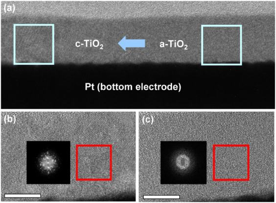
Figure 6. (a) TEM image showing the transition region from amorphous TiO2 to crystalline TiO2 after positive bias sweep up to +7 V. (b), (c) High-resolution images from crystalline and amorphous TiO2, respectively, the FFTs of which show a poly-crystalline pattern and an amorphous broad ring pattern. The scale bar is 10 nm.
Download figure:
Standard image3.5. Early stages of electroforming
Therefore, a plausible explanation can be given as follows. In the first bias sweep, the less defective surface deformation layer may need a higher critical bias to activate electrochemical processes and corresponding measurable strains due to the surface oxide layer. However, once the entire volume along the thickness direction is electrochemically active during the first bias sweep, then the electrochemical behavior becomes nearly identical for both the inside and the outside of the disks. Nevertheless, since there is an additional surface layer on the surface deformed area, the electrical behavior can be different, as seen in figure 4(d).
On the basis of experimental results as well as previous reports, electroforming procedures under positive bias sweep to the conductive probe are expected to be described as follows (see figure 7).
- (1)Local electrochemical reactions, i.e. oxygen vacancy formation, occur underneath the AFM tip (figure 7(a)(ii)). However, there is no significant oxygen vacancy movement and/or electron injection.
- (2)Both electron injection from the bottom electrode and oxygen vacancy movement from the film surface induce current flow, resulting in local Joule heating (figure 7(a)(iii)).
- (3)Joule heating induces crystallization of TiO2, e.g. brookite, anatase, rutile, and/or Magnéli (figure 7(a)(iv–v)).
- (4)The surface oxidation, which is relevant to the NDR, occurs during the crystallization process of stage (3) (figure 7(a)(vi)).
- (5)As the positive bias voltage keeps increasing, a conductive filament can be formed along the thickness direction, so called complete electroforming (not shown here).
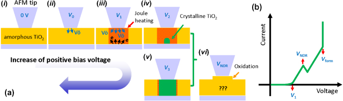
Figure 7. Schematics of (a) the stages of electroforming under positive bias sweep using an AFM tip: (i) pristine amorphous TiO2, (ii) the beginning of the electrochemical reaction, (iii) the beginning of Joule heating, (iv)–(v) crystallization of TiO2, and (vi) surface oxidation—it occurs during the crystallization process. (b) The corresponding I–V curve.
Download figure:
Standard image4. Conclusions
In summary, we have investigated the local electrical/electrochemical behavior at the early stage of electroforming in TiO2 memristive materials. NDR during positive bias sweeps and corresponding surface deformations was observed below the electroforming voltages by CAFM measurements. The surface deformations induced by oxidation are thermodynamically stable, reversibly controlled by applying different polarity of the bias sweeps, and electrochemically less active at the early stage of bias sweep. In addition, combined analysis of CAFM and ESM shows that electrochemical reactions occur at lower bias voltage before current flows. Hence, the present results allowed us to understand the NDR and its electrochemical processes over all the stages of electroforming in memristive materials.
Finally, we illustrated the combination of CAFM and ESM to separate and probe dissimilar stages of bias-induced transformations in solids. The approach of combination of CAFM, ESM, and TEM can be synergic on the study of memristive systems (reversible and irreversible components), fuel cell materials, and other electrochemically functional solids. We further note that the high spatial resolution of these methods suggests that systems with well-defined isolated defects can be studied, opening a pathway for probing electrochemical functionalities on a single-defect level.
Acknowledgments
This research was supported (SVK, YK, AYB) by the US Department of Energy, Basic Energy Sciences, Materials Sciences and Engineering Division. Portions of this research were conducted at the Center for Nanophase Materials Sciences (SVK, SJ), and the ShaRE user facility, which are both sponsored at Oak Ridge National Laboratory by the Scientific User Facilities Division, Office of Basic Energy Sciences, US Department of Energy. This work was supported by the Korea Research Council of Fundamental Science and Technology through the KRISS project and in part by the Future-based Technology Development Program (Nano Fields) through the National Research Foundation of Korea (NRF) funded by the Ministry of Education, Science and Technology (Grant No. 2011-0030200). This work (JHJ) was supported by a grant from the National Research Foundation of Korea (NRF) funded by the Ministry of Education, Science and Technology (Grant No. 2012-0005637).