
Abstract
We report a simple lithography-free, solution-based method of soldering of carbon nanotubes with Ohmic contacts, by taking specific examples of multi-walled carbon nanotubes (MWNTs). This is achieved by self-assembling a monolayer of soldering precursor, Pd2+ anchored to 1,10 decanedithiol, onto which MWNTs could be aligned across the gap electrodes via solvent evaporation. The nanosoldering was realized by thermal/electrical activation or by both in sequence. Electrical activation and the following step of washing ensure selective retention of MWNTs spanning across the gap electrodes. The soldered joints were robust enough to sustain strain caused during the bending of flexible substrates as well as during ultrasonication. The estimated temperature generated at the MWNT–Au interface using an electro-thermal model is ∼150 °C, suggesting Joule heating as the primary mechanism of electrical activation. Further, the specific contact resistance is estimated from the transmission line model.
Export citation and abstract BibTeX RIS
1. Introduction
One-dimensional (1D) nanomaterials are promising for many applications including biosensors, gas sensors, lasing, photonics, nanoelectronics and optoelectronics [1, 2]. The electronic circuits made with 1D nanomaterials often lack robust contacts leading to high contact resistance that can dominate over their intrinsic resistance. High-performance devices, such as field-effect transistors, are achieved by different bonding processes that yield Ohmic contacts with minimum contact resistance [3, 4]. For example, contact resistance can be reduced by depositing electrodes on top of 1D nanomaterials using approaches such as electron beam lithography (EBL) [5], but these patterning approaches can cause deleterious effects from contamination during processing. Further, fabrication of large-scale integrated circuits using EBL is rather slow and expensive.
Conversely, several different techniques have been attempted for soldering of 1D nanomaterials such as rapid thermal annealing [6], electron (or focused ion) beam induced metal deposition (EBID or FIBID) [7] and solder reflow [8]. Rapid thermal annealing is a harsh method and is not amenable to flexible substrates such as PET (polyethylene terephthalate). On the other hand, EBID and FIBID can cause diffusion of the solder into the 1D nanomaterial being soldered and thus can affect its electrical properties [7, 9]. However, such physical methods are expensive and not pliable to large areas. Although solder reflow [8, 10] is a reliable method for soldering positioned 1D nanomaterials between electrodes, it is tedious and not tractable to all nanoscale structures as the process involves integrating the solder segments to 1D nanomaterials during the synthesis. Hence, a solution-processed method with minimal contamination is of great importance to solder 1D nanomaterials.
Among 1D nanomaterials, carbon nanotubes (CNTs) have gained a great deal of importance, because of their unique electrical, mechanical and other outstanding properties [11]. The soldering of CNTs across gap electrodes was demonstrated by taking the example of multi-walled carbon nanotubes (MWNTs) which can sustain high current densities with potential applications in power transmission [12], IR detectors [13], transparent conducting electrodes [14] etc. Such applications require a simple lithography-free method to solder MWNTs with minimal contact resistance to realize high-performance devices. On the other hand, the present approaches have had limited success particularly with regard to flexible applications as the CNT junctions in circuits may not be robust enough to sustain bending [15]. In the literature, CNTs have been soldered across gaps by methods such as ultrasonic welding [16], and electroless deposition on electrodes to reduce the contact resistance [17]. Also, local Joule heating along the interface of the CNT–electrode has been proposed for minimizing contact resistance [18], but during the process, the oxidation of outer shells leads to rupture and damage of MWNTs [12, 19–21]. Hence, the conductance of CNTs in air is limited by a threshold power above which oxidation occurs. Facile methods to solder CNTs across gaps with minimum contact resistance remain a crucial need if individual CNT properties are to translate into useful collective functions.
Previously, we developed an EBL method to solder MWNTs across a gap with Pd hexadecanethiolate as a soldering precursor [22]. Pd was chosen as a nanosoldering material for MWNTs, as it is known to form Ohmic contacts [23]. In this work, we have formulated a simple lithography-free solution-based method by which MWNTs can be soldered electrically using a monolayer of Pd precursor self-assembled on the electrode surface. The process ensures selective soldering of the CNTs and the unsoldered ones can be recycled. The soldered joints can withstand substrate bending. An electro-thermal model, transmission line model and Simmons electron tunnelling model have been employed to obtain a mechanistic insight of the soldering process.
2. Experimental section
Au gap electrodes (50 nm thick) were deposited on glass substrates using a thin carbon fibre as a shadow mask by physical vapour deposition with gaps typically 6 μm wide. As-deposited Au gap electrodes were cleaned with water, acetone and isopropyl alcohol just before the self-assembly. Subsequently, the substrates were immersed in a 50 mM solution of 1,10 decanedithiol in toluene for 2 h; non-chemisorbed dithiol was washed away by excess toluene. Afterwards, the substrates were dipped in a 25 mM Pd2+ acetate in toluene solution for 1 h and washed in toluene. Multi-walled carbon nanotubes (Sigma Aldrich) of diameters 150–300 nm and lengths 4–12 μm were used as active elements across the Au gap electrodes. The MWNTs were dispersed in o-dichlorobenzene by ultrasonication for 15 min. o-dichlorobenzene is considered as a good dispersing medium for the MWNTs and leaves minimal solvent traces after evaporation [24]. The current–voltage measurements of the circuits were performed using a Keithley 236, which served as the source and measurement unit. SEM was carried out using a Nova NanoSEM 600 instrument (FEI Co., The Netherlands). The contact length of the MWNTs was estimated from the SEM images. AFM measurements were performed using a Dimension 3100 SPM with an NS-IV controller (Bruker, USA) in contact mode. Standard Si cantilevers were used for normal topography imaging. The sample for Fourier transform infrared (FTIR) spectroscopy was prepared by drop-casting (1 mM) Pd decanethiolate in toluene on a KBr pellet followed by evaporation of the solvent. The FTIR spectra of the Au surface covered with Pd/SAM layers and a thin film of Pd decanethiolate on the KBr pellet were taken in reflection mode. The FTIR measurements were recorded using a Bruker IFS66v/s spectrometer with a resolution of 2 cm−1. X-ray photoelectron spectroscopy (XPS) measurements have been carried out using a Omicron SPHERA spectrometer with non-monochromatic Al Kα (E = 1486.6 eV).
3. Results and discussion
The soldering ingredients are introduced via self-assembly across a pair of Au electrodes (separated by ∼6 μm, see figure 1(a)). A self-assembled monolayer (SAM) of 1,10 decanedithiol is adsorbed firstly on Au electrodes (see figure 1(b)) and decorated subsequently with Pd2+ (figure 1(c)), which constitutes the soldering precursor, i.e., Pd/SAM. Further, CNTs are aligned across the Au gap electrodes covered with Pd/SAM solder (figure 1(d)). The soldering of the as-prepared device was activated at first electrically (see figure 1(e)), following which the substrate is subjected to ultrasonication to remove un-activated CNTs (not spanning the gap electrodes). The soldering process was completed by thermolysing the activated precursor at 250 °C (see figure 1(f)). The method is extendable to flexible substrates as well and the solder joints are robust enough to take the strain caused during the bending (see figure 1(f)).

Figure 1. Schematic illustration of the fabrication of a soldered CNT circuit: (a) 6 μm Au gap electrodes (∼50 nm thick), (b) covered with a SAM after immersion in 1,10 decanedithiol solution, followed by (c) decoration of Pd2+ onto the SAM from a Pd acetate solution. (d) CNTs assembled across the gap electrodes and (e) electrical activation for soldering; (f) ultrasonication and heating of the CNT circuit for removal of unwanted CNTs. The method is extendable to flexible substrates as well.
Download figure:
Standard imageInitially, a detailed characterization of the self-assembled soldering precursor layer on Au electrodes was performed (figure 2). The AFM topography of the Pd/SAM/Au electrode in figure 2(a) reveals the uniformity of the soldering precursor with the roughness being ∼1.2 nm, which may be compared with the roughness values from pristine Au and SAM/Au surfaces, 0.5 and 0.9 nm respectively (see figures 1(a), (b) and SI figure S1 (available at stacks.iop.org/Nano/24/075301/mmedia) for AFM images of pristine Au and SAM/Au substrates). The increase in roughness of the Au electrodes with sequential addition of SAM and Pd2+ layers is consistent with nanometric agglomeration of the soldering precursor seen in the AFM image (see figure 2(a)). An increase in roughness with SAM thickness has been reported previously [25]. The FTIR spectrum of the Pd/SAM/Au electrode in figure 2(b) exhibits peaks at 2850 and 2920 cm−1 corresponding to symmetric (d+) and anti-symmetric (d−) stretching vibrations of the methylene group respectively, typical of trans-conformation of the SAM [26]. This spectrum is compared to that of pristine Pd decanethiolate to assess order and crystallinity in the Pd/SAM layer. A blue shift of ∼4 cm−1 is observed for the d− peak in the case of Pd/SAM which signifies the presence of gauche conformers in chemisorbed SAM [27]. Figure 2(c) elucidates the Raman spectrum of Pd/SAM, where the deconvoluted peaks at 257 and 306 cm−1 correspond to the stretching modes of Au–S and Pd–S bonds respectively [28, 29]. Thus, the Raman spectrum reaffirms the bonding of molecules with Au beneath and Pd on top (see figure 1(c)).
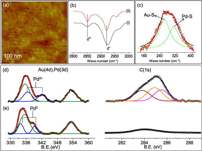
Figure 2. Characterization of Pd/SAM covered Au electrodes. (a) AFM topography image. (b) FTIR spectra of Pd/SAM/Au (intensity has been multiplied by 3) (i) and pristine Pd decanethiolate (ii). (c) Raman spectrum (red circles) with the deconvoluted peaks (in green) corresponding to Au–S and Pd–S stretching modes. Core level photoelectron spectra of Pd 3d, Au 4d and C 1s before (d) and after heating (e) at 250 °C (blue, green, black deconvoluted peaks represent Pd 3d, Au 4d and C 1s respectively).
Download figure:
Standard imageIn order to determine the oxidation state of the Pd present on top of the SAM layer, x-ray photo emission spectroscopy (XPS) measurements were carried out on the self-assembled soldering precursor before and after thermolysis. The core level spectra of Pd 3d and Au 4d are observed close to each other due to their similar binding energies and therefore, the obtained spectra were deconvoluted from the observed broad peak as shown in figures 2(d) and (e). The peaks at ∼336.5 and ∼342 eV (figure 2(d)) corresponding to Pd 3d5/2 and 3d3/2, respectively, are indicative of the Pd2+ species resident on the SAM layer [30]. The soldering action (metallization) of the Pd/SAM layer was also examined first with a control sample without CNTs. As expected, Pd2+ reduces to Pd metal after thermolysis [31] with the peaks shifting to lower binding energies (3d3/2 ∼ 339.25 and 3d5/2 ∼ 334 eV, see figure 2(e)). Of course, Au 4d core level features, 4d3/2 ∼ 353.4 and 4d5/2 ∼ 335.5 eV, respectively corresponding to the Au substrate [32] remain unchanged (see figure 2(e) left panel). The C 1s core level spectrum before thermolysis is comprised of three peaks as shown in figure 2(d) (right panel), which are positioned at 283.8, 284.9 and 285.4 eV corresponding to sp2-hybridized carbon, C–C and C–S bonds, respectively [33, 34]. After heating to 250 °C, only one peak assignable to trace carbon was present at 284.1 eV while the other peaks disappeared (see figure 2(e) right panel). Notably, the C 1s peak intensity decreased by three times, confirming desorption of the SAM. The S 2p signal indicates the presence of both Pd–S and Au–S bonds before thermolysis (see SI figure S2 available at stacks.iop.org/Nano/24/075301/mmedia). Through these measurements, we confirm that thermolysis involves desorption of the SAM and concomitant conversion of Pd2+ to metallic Pd.
A dispersion of CNTs in o-dichlorobenzene was drop-casted on pre-characterized Au electrodes covered with a Pd/SAM layer (see figure 2) heated at 80 °C for slow evaporation of solvent. The dispersed CNTs are dragged towards the gap as a result of the capillary force exerted by the solvent frontline during evaporation. The dragged CNTs span across the gap leading to self-alignment, which has been discussed in the literature [35]. We employed this method to align as many as 12 CNTs across a single Au gap electrode as shown in SI figure S3 (available at stacks.iop.org/Nano/24/075301/mmedia). We have examined several Pd/SAM/Au electrodes dosed with CNT dispersions which showed similar results. One such configuration is shown in figure 3(a), where five CNTs bridge across the gap; the inset clearly reveals that the CNT spans the gap between electrodes. The I–V characteristics of this circuit were slightly non-linear (figure 3(b)) with estimated resistance from the near zero bias region of 97 kΩ. This high value arises mainly due to the insulating nature of the SAM. The device was thermally activated by heating at 250 °C for 45 min to desorb the SAM (see SI figure S4 available at stacks.iop.org/Nano/24/075301/mmedia). Thereafter, the current in the circuit increased, implying that soldering by thermal activation decreased the contact resistance, and the I–V characteristics became linear, suggesting the Ohmic nature of the contacts (figure 3(c)). The resistance reduced by nearly two orders to ∼1.8 kΩ. This result clearly indicates thermal soldering mitigated the ultra-high contact resistance introduced by the SAM. However, the Pd/SAM soldering precursor is essential, without which thermal treatment does not lead to Ohmic contacts (see SI figure S5 available at stacks.iop.org/Nano/24/075301/mmedia).

Figure 3. (a) SEM image of the CNT circuit after self-assembly of CNTs with the inset showing a magnified view of a single CNT across the gap. I–V characteristics of the self-assembled CNT circuit before (b), after heating (c) at 250 °C.
Download figure:
Standard imageWhile the above process of using a SAM as a carrier for the Pd soldering precursor leads to Ohmic contact between CNTs and the electrodes, the resultant structure lacks specificity. In other words, CNTs lying away from the electrical gap not participating in conduction are also glued to the electrode surface, which results in wastage of CNTs. A more desirable process could selectively solder CNTs spanning across the electrodes, enabling the retrieval of other CNTs. With this in mind, electrical activation of the soldering precursor was attempted (see figure 4). In the circuit shown in figure 4(a), individual CNTs and bundles of CNTs are shown in rectangles and circles, respectively. Three CNTs lie near the gap of the electrodes, out of which the CNT labelled '1' neatly spans across the gap electrode (see the inset for a magnified view). The I–V characteristic of the pristine CNT circuit exhibited a resistance of 1.72 MΩ (figure 4(b)). Here, the electrical activation is achieved by applying a low voltage bias. To determine the optimal voltage bias, several bias values were tried out. In circuits activated with high bias (∼6 V), CNTs were blown off, rupturing the electrodes (see SEM in SI figure S6 available at stacks.iop.org/Nano/24/075301/mmedia) due to the high power generated at the CNT–Au interface [18, 21]. For this reason, the circuit was activated at a lower bias (2 V) for a short time (15 s). Interestingly, the current in the circuit increased by two orders of magnitude after electrical activation (see figure 4(c)). Two possible effects may lead to this behaviour, Joule heating and electrical migration; here, an electro-thermal model is therefore considered (vide infra, also see SI note 1 available at stacks.iop.org/Nano/24/075301/mmedia).

Figure 4. SEM image of CNTs on Au gap electrodes (a) before ultrasonication, marked areas show randomly distributed CNTs and (d) after ultrasonication, marked areas do not possess CNTs. I–V characteristics of the pristine CNT circuit (b) before, (c) after electrical activation, (e) followed by ultrasonication for 30 s and (f) finally heating at 250 °C.
Download figure:
Standard imageFollowing electrical activation, unsoldered CNTs and extraneous carbon material can be removed by mild ultrasonication of the substrate in o-dichlorobenzene for 30 s. The electrically activated CNTs were found to be intact with the Au electrodes even after ultrasonication, as shown in figure 4(d) (also see figures S7 and S8 available at stacks.iop.org/Nano/24/075301/mmedia). The CNTs that do not span the gap electrode were washed away during ultrasonication and can be reused for the fabrication of new CNT circuits. Notably, the decrease in current after ultrasonication (figure 4(e)) is due to the removal of one of the self-assembled CNTs spanning the gap electrode in addition to the presence of solvent traces. Its removal suggests that only weak electrical activation occurred for this CNT, maybe due to its relatively high resistance (the removal of the CNT is shown in SI figure S9 available at stacks.iop.org/Nano/24/075301/mmedia). The current in the circuit was enhanced following heating the circuit at 250 °C for 30 min (figure 4(f)). The resistance of the CNT circuit was 2.5 kΩ after thermal activation, which decreases the resistance by nearly two orders. Thus, the electrical and thermal activation were combined to selectively solder the CNTs spanning across the gap. However, the former alone may not be practical for circuits containing many CNTs, as the current required to cause complete soldering will be proportionally very high and can lead to damage of CNTs.
In order to investigate the electrical activation process in detail, a circuit with only one CNT spanning across the gap was fabricated. The SEM image of the CNT shown in the inset of figure 5 clearly shows the CNT spanning across the gap with a contact length of 2.72 ± 0.1 μm on the electrodes. The initial resistance of the single CNT circuit was ∼100 kΩ due to the presence of insulating species prior to soldering. Current controlled experiments were performed in order to prevent thermal runaway during the transient drop in contact resistance that occurs during electrical activation. For this purpose, a variable current source was ramped at a constant, controlled rate of 5 mA s−1, and the transient resistance change was measured. Initial tests with maximum currents of 10, 20 and 100 μA displayed a measurable change in resistance, which interestingly reversed to the initial value upon withdrawal of the current (see the SI figure S10 available at stacks.iop.org/Nano/24/075301/mmedia). As shown in figure 5, the application of 1–1000 μA decreased the resistance permanently by ∼20 times, suggesting that electrical activation occurred in the current range of 100–1000 μA. The resistance of this circuit decreased permanently from 100 to 3.6 kΩ after the electrical soldering; the reduction in resistance here compares well with that obtained via thermal soldering. It demonstrates that the above method of current controlled activation would suffice for simple circuits with a single CNT such as the one shown in figure 5, while circuits containing multiple CNTs may additionally require the following step of thermal treatment to achieve lower contact resistances. This is not surprising because parallel-channel devices would not be expected necessarily to exhibit equal resistances in each channel. Therefore, the Joule heating would be non-uniform, resulting in high variations in activation. Between the two types of electrical activations, current controlled activation is considered superior as there is less chance of overloading and rupturing of the electrodes (compare SI figures S6 and S10 available at stacks.iop.org/Nano/24/075301/mmedia); but this is applicable effectively only for single CNT circuits. A summary of the CNT circuits fabricated in this study is given in ESI, table S2 (available at stacks.iop.org/Nano/24/075301/mmedia).

Figure 5. Resistance of a single CNT circuit as a function of current during (black) and after (red) the electrical activation. The inset shows the SEM image of the CNT spanning across the Au gap electrodes self-assembled with a Pd/SAM layer.
Download figure:
Standard imageTo assess the dominant mechanism of electrical activation, a simplified electro-thermal model is considered as depicted in figure 6. In this model, only the electrically and thermally active region of the SAM is considered and thermal boundary resistance between the CNT and Au substrate is neglected [36]. In other words, the highly insulating SAM layer prohibits current flow laterally across the SAM, forcing current to flow vertically across the SAM through the CNT contact. The Joule heat generated in the SAM is expected to induce its desorption in the activation region (figure 6(b), dashed area), enabling Pd to aggregate at the CNT–Au interface, as shown in figure 6(c). Under conditions of steady electrical current and heat flow, the temperature of the SAM–CNT interface (TSAM) results from Joule heat generation per unit area P'':

where G'' is thermal conductance per unit area of the SAM–CNT interface and TAu is the electrode temperature. The thermal conductance (G'') of the Au–SAM was considered to be 220 ± 100 μW μm−2 K−1 based on the literature value of experimentally measured conductance of an alkanethiol functionalized Au surface [37]. The contacting perimeter between the SAM and CNT was estimated as 32 ± 1 nm for the ∼160 nm diameter (see SEM image figure 5), assuming perfect conformation of the SAM on the CNT surface (see SI figure S11 for more details available at stacks.iop.org/Nano/24/075301/mmedia). The CNT–SAM contact area is therefore estimated as 0.087 ± 0.003 μm2, based on the length and perimeter of the contact. The average heat energy generation rate and temperature rise of the SAM were calculated as a function of source current from the experimental electrical activation data (figure 5) based on the above described theory, and the result is shown in figure 6(a). As shown in the plot, the temperature bounds (red dashed curves) suggest that the temperature of the SAM increases with increase in current. In contrast to the thermal treatment (250 °C, 45 min), the duration of the entire electrical activation experiment was short (0.2 s). Thus, only a small portion of the SAM at the SAM–CNT interface could be desorbed from the local Joule heating (see figures 6(c) and 1(e)), and this resulted in electrical connection between the Au electrode and the CNT through Pd. This finding supports the conjecture that electrical activation occurs via a localized Joule heating mechanism. For a deeper insight into the details of the electrical activation mechanism, the Simmons electron tunnelling model [38] was applied for this circuit to assess the electronic transport regimes before and after electrical activation (see SI note 2 for more information available at stacks.iop.org/Nano/24/075301/mmedia). The interfacial gap was estimated to be ∼2.1 nm from the I–V characteristics of the circuit as shown in SI figure S12(a) (available at stacks.iop.org/Nano/24/075301/mmedia), which indicates that the interfacial gap is roughly comparable to the length of the 1,10 decanedithiol molecule (∼1.4 nm) [39]. As shown in the schematic of figure 6(b), the CNT is supported on top of the SAM distributed with Pd2+. After electrical soldering the fitted interfacial gap is 0.13 nm (see SI figure S12(b) available at stacks.iop.org/Nano/24/075301/mmedia) suggesting a good (metallic) bond between the CNT and the electrodes (see figure 6(c)). Sufficient electrical heating desorbs SAM molecules in the electrically active region; thereby the Pd solder forms at the CNT–Au interface. Thus, the electrical activation decreased the interfacial gap to form good electrical contact.
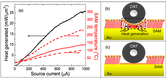
Figure 6. (a) Heat generation and SAM temperature at the CNT–Au interface as a function of source current during electrical activation of a CNT circuit. Theoretically predicted SAM temperature (solid red line) has bounds due to uncertainty of Au–SAM thermal conductance indicated by dashed red lines. Schematic illustration of the CNT circuit (b) before (the dashed rectangle encloses the activation region) and (c) after electrical activation.
Download figure:
Standard imageThe electrical resistance of the soldered circuit, i.e, total resistance, comprises the actual resistance of the CNT (RCNT) and specific contact resistance (rc). To estimate the actual resistance of the CNT, a transmission line model was applied as described by Lan et al [40]. The contact length of the single CNT circuit was calculated from the SEM image as shown in figure 7(a). The plot between the total resistance and contact length of six single CNT circuits is shown in figure 7(a) (black circles, blue circles represent thermally and electrically soldered circuits respectively). The red curve is the best fit for the data, and the estimated parameters are the CNT resistance (RCNT), 0.16 ± 0.02 kΩ μm−1 and specific contact resistance (rc), 1.92 ± 0.15 kΩ μm−1 (see SI note 3 for more information available at stacks.iop.org/Nano/24/075301/mmedia). As shown in figure 7(a), the decrease in total resistance with contact length was significant and suggests that the transport in the circuit was not dominated by contact resistance, thereby establishing the efficacy of our soldering recipe. A length-independent measure of contact resistance, specific contact resistance rc, is also considered to quantify the CNT binding quality obtained by the present electrical activation process. The specific contact resistance is defined as rc = RcL, where Rc is the total contact resistance in kΩ and L is the CNT contact length in μm. As this parameter is a length-independent measure of contact resistance, it provides an intrinsic metric to compare the soldering quality of CNTs of differing sizes and for varying bonding electrode materials. In figure 7(b), the specific contact resistance obtained with the present electrical soldering process is compared to those obtained via conventional metal deposition. CNTs of various sizes have been bonded and their linear contact resistivity values have been presented previously [40, 41]. As depicted in figure 7(b), the present bottom-up process yields specific contact resistance near the low end of the distribution of contact resistances from the literature. With such low linear contact resistivity, integration of the present facile fabrication process may be rapidly achieved for CNT circuit fabrication.
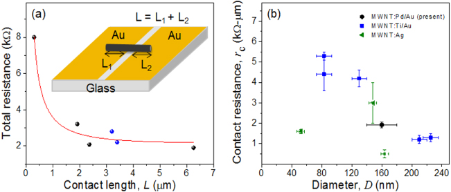
Figure 7. (a) Total resistance versus contact length of single CNT circuits. The solid circles represent experimental data; the solid line is the best fit for resistance from a transmission line model [40]. (b) Linear contact resistivity as a function of CNT diameter soldered via different processes. The legend indicates the type of CNT–metal bond. Data for CNT: Ti/Au and CNT: Ag are depicted from [40, 41].
Download figure:
Standard imageThe present soldering process was extended to flexible substrates (kapton, 6 μm gap electrodes) as well. Figure 8(a) shows the I–V characteristics of a CNT circuit, containing two CNTs soldered to the electrodes. There is minimal change in the I–V characteristics after five bending cycles, demonstrating the robustness of the soldered circuit. A careful examination of the circuit using SEM (SI figure S13 available at stacks.iop.org/Nano/24/075301/mmedia) showed that the CNT was intact across the Au electrodes at a bending diameter of 1 cm. The traces shown in the top inset in figure 8(a) expose a relatively small change in the position of the CNT while the soldered regions are unaffected. Many such circuits have been tried out in bending experiments (table S3 available at stacks.iop.org/Nano/24/075301/mmedia). The small changes in the CNT geometry across the gap do reflect in the circuit resistance (figure 8(b)). The resistance is observed to increase with bending diameter of the substrate, in both compression and tension, which is attributed to the incremental strain in the CNT (unlikely at the soldered interface), which is consistent with the literature [42]. The gauge factor for the various circuits was in the range of 0.57–6.28, which is comparable to the values observed in the case of MWNT/epoxy nanocomposite (GF ∼ 10) [43]. Metallic CNTs are known to exhibit weak sensitivity to strain [44]. The change in resistance is minimal after making the circuit flat (at infinity diameter) following a bending cycle (see figure 8(b)). This indicates that the soldered contact between the CNTs and the Au electrodes is robust, which is an essential requirement for high performance flexible electronics.
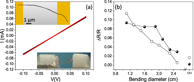
Figure 8. (a) I–V characteristics of the soldered CNT circuit before (red curve) and after five bending cycles (black curve); the top inset shows the trace of SEM images, flat (solid line) and bended (dotted line), and the bottom inset shows a photograph of a flexible CNT circuit. (b) Change in resistance of the CNT circuit with respect to bending diameter; compression and tension data are represented by solid circles and open circles respectively.
Download figure:
Standard image4. Conclusions
A simple lithography-free, solution-based method to assemble and solder carbon nanotubes across a gap was investigated. The soldering precursor, Pd2+ anchored to 1,10 decanedithiol, was introduced onto the electrodes by a self-assembly process. The nanosoldering has been carried out by thermolysis as well as by electrical activation. In thermal activation, the substrate is heated to desorb the molecules leading to the formation of Ohmic contacts between the CNTs and the electrodes with minimal contact resistance. In electrical activation, selective soldering of nanotubes was ensured by means of self-heating at the contacts, by Joule heating, i.e., local thermolysis, leaving behind a conductive metal contact. The temperature generated at the interface between the CNTs and electrodes is estimated to be ∼150 °C. The unwanted carbon material and unsoldered CNTs not spanning across the gap were removed by ultrasonication. The method proposed here is highly selective in soldering only the active CNTs across the gap implying that the neatness of the circuit is maintained and parasitic conductance paths via randomly laid CNTs can be avoided. The current controlled activation is better than the voltage controlled activation to avoid thermal runaway of the circuits. The specific contact resistance estimated from the transmission line model is compared to the lower values found in the literature. The flexibility of the soldered circuit is shown at various bending diameters, while the soldered joint is unaffected. The method is generic and should be applicable to 1D nanomaterials, in general.
Acknowledgments
The authors are grateful to Professor C N R Rao for his encouragement. The authors thank N Kurra, R Gupta and V S Bhadram for technical assistance. The financial support from the Department of Science and Technology, Government of India, is gratefully acknowledged. KDMR and BR thank UGC and CSIR respectively for their fellowships. The authors thank the Indo-US Science and Technology Forum for supporting collaboration visits between our respective institutions.