
Abstract
Graphane, hydrogenated graphene, can be patterned into electronic devices by selectively removing hydrogen atoms. The most simple of such devices is the so-called nanoroad, analogous to the graphene nanoribbon, where confinement—and the opening of a gap—is obtained without the need for breaking the carbon bonds. In this work we address the electronic transport properties of such systems considering different hydrogen impurities within the conduction channel. We show, using a combination of density functional theory and non-equilibrium Green's functions, that hydrogen leads to significant changes in the transport properties and in some cases to current polarization.
Export citation and abstract BibTeX RIS
1. Introduction
Since its synthesis in 2004 [1] graphene has drawn a lot of attention from the scientific community [2–4]. Mainly due to its unique geometry (a single layer of carbon atoms) [1] it has tantalizing mechanical [5], thermal [6], electronic [4] and transport [7] properties. The greatest issue hindering the use of graphene as an electronic device, however, is the absence of a intrinsic band gap. Thus far, opening a gap on its band structure has been a difficult task [8]. A proposed alternative is to confine the system into a one-dimensional structure, then a band gap opening due to quantum effects is expected [9]. In order to do that several paths to synthesize graphene stripes, known as graphene nanoribbons (GNRs), have been tried; chemical [10], carbon nanotube unzipping [11, 12], lithographic [13] and ion implantation on SiC [14] are a few examples. Albeit lithographic patterning is promising for large scale production – since it is a well established technique – it faces problems with edge smoothness and width control, connected to limitations in the technique's resolution.
A different single layer material called graphane [15], formed by fully hydrogenated graphene, can also be patterned using a lithographic technique [16]. In this case hydrogen atoms are selectively removed from the structure forming a graphene-like region. The main advantage here is that the overall structure would remain two-dimensional, and thus easier to integrate in a circuit. This patterned graphane, the so-called nanoroads, was previously proposed and studied by Singh et al [17]. They found that the graphene nanoroads mimic some of the isolated GNRs' properties, such as band gap and magnetic ordering.
Albeit the synthesis of the nanoroads is possible [16], perfect edge smoothness could still be a problem—in a manner similar to isolated GNRs—for synthesis. At the nanoscale, even a single impurity could alter the system's electronic and transport properties. In particular, as a result of the fabrication process, hydrogen impurities and vacancies might be present in the system. Thus it is important for device fabrication to determine the effects of such defects.
In order to assess the viability of nanoroads as electronic devices we performed ab initio electronic transport calculations, by means of density functional theory [18, 19] coupled to Green's function methods (GF) [20, 21]. We have simulated systems containing several types of H impurities or vacancies. We have observed a high attenuation on the transmittance of almost all systems in the presence of impurities; even a wider system has shown a perceptible attenuation. Thus the presence of impurities significantly alters the transport properties of the nanoroads, hindering its applications to electronic devices.
2. Methodology
The system used in our calculations is a patterned graphane in which the central region has no hydrogen atoms, forming a nanoroad with armchair edges. The calculation the simulation cell used was 26.35 Å long (6 unit cells) and 15.11 Å wide (8 unit cells), and the actual nanoroad – the hydrogen-free region – was 7.57 Å wide, as shown in figure 1. We have also simulated a wider nanoroad, of 17.45 Å width, in order to evaluate size effects on the system. The nanoroads simulated are quite narrow, but to study single/few atoms defects the systems are suitable. We can extrapolate the behavior of larger systems from the results obtained in our calculations. We also expect some similarities with the behavior of nanoribbons with edge disorder. Mucciolo et al [22] and Evaldsson et al [23] have studied disorder effects in graphene nanoribbons. They observe conductance suppression even for a small amount of defects. We expect to see similar effects for the nanoroads studied.
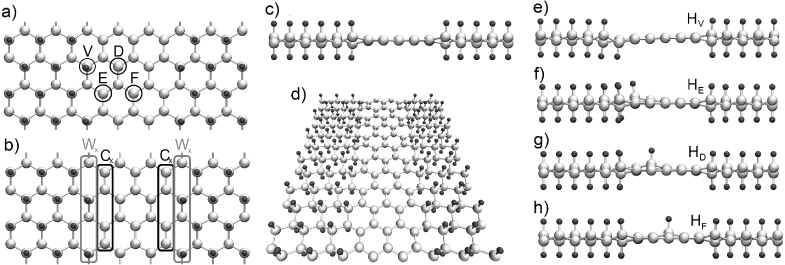
Figure 1. Image showing the various configurations of the patterned graphene (nanoroads) used in our calculations. In (a), (c) and (h) the pristine nanoroad is shown. In (a) the defect sites are indicated by the letters above the circles. In (d)–(g) the defective nanoroads are shown. The dark colored atoms are hydrogen and the light colored ones are carbon. The cell sizes are 26.35 Å long and 15.11 Å wide. The central region is a 7.57 Å wide nanoroad.
Download figure:
Standard image High-resolution imageFor the transport calculations we divided our system into three regions, a central scattering region connected to two semi-infinite electrodes [24]. The electrodes were chosen to be nanoroads with the same width as the scattering region. To obtain the transmittance we used a Landauer–Büttiker-like formula, based on the GF method [25, 26], within the two-spin fluid approximation (neglecting spin–orbit interactions).
For our DFT calculations we employed the SIESTA [27, 28] computational code. In this work we have used a double zeta basis set with polarization orbitals, and the generalized gradient approximation (GGA)—as parameterized by Perdew–Burke–Ernzerhof [29] (PBE)—for the exchange–correlation functional. The atomic coordinates were relaxed until forces were lower than 0.03 eV Å−1.
In this work we have initially explored three different positions for an extra H: on the edge (HE), right after the edge (HD) and at the center of the nanoroad (HF), as shown in figure 1(a). We also considered a nanoroad with a single H atom removed, a hydrogen vacancy (HV). Finally, we also explored the behavior of either constricted or quantum-dot-like configurations in the system. The constricted (CX) arrangements were obtained by removing either a single line of four atoms (C1) on one edge, or two lines (C2) on each side (figure 1(b)). Analogously the widened regions (WX) are formed by removing 4 (W1) and 8 atoms (W2), respectively.
In order to access the stability of these defective systems we have calculated the binding (Eb) and formation energies (Ef) per H atom:


where ETH is the total energy of the defective system, ETC is the total energy of the clean system (with a nanoroad), N is the number of inserted (removed) hydrogen atoms, ETHA is the total energy of a single isolated hydrogen atom and μH2 is the total energy per atom for a H2 molecule. The ∓ sign indicates respectively whether atoms have been added (constriction) or removed (widened nanoroad).
3. Results
From our calculations we infer that the three positions considered for the extra hydrogen are stable, as can be seen from the negative binding energies in table 1, with higher values near the edge. At the same time the formation energies are positive, meaning that it is unfavorable for a H2 molecule to dissociate and then bind to the interface. These results are in line with calculations by Li et al [30]. The results for the addition (removal) of two hydrogen atoms indicate that the introduction of pairs of hydrogen atoms is more likely and also shows a tendency towards a fully hydrogenated graphane structure as being the most stable one. These results indicate that the dehydrogenation process in graphene is most likely to lead to defects.
Table 1. Binding (Eb) and formation energies (Ef) of the constrictions, widened nanoroads and single hydrogen defects, calculated with equations (1) and (2).
| Structure | Eb (eV) | Ef (eV) |
|---|---|---|
| HE | −1.78 | 0.36 |
| HD | −1.29 | 0.84 |
| HF | −0.68 | 1.46 |
| HV | 3.43 | 1.29 |
| C1 | −2.53 | −0.39 |
| C2 | −2.54 | −0.39 |
| W1 | 7.32 | 5.18 |
| W2 | 5.13 | 2.98 |
The transmittances for single H systems are plotted in figure 2 and, except for the HF case, they are highly attenuated. In the HF case the mirror symmetry present in the original system is restored. We can see from figure 3(a) that the level inserted by the hydrogen atom (indicated by letter d), does not interact with the delocalized levels of the pristine nanoroad. This is noted also in the wavefunctions at the Γ point, plotted in figures 3(b)–(d). The pristine bands, (b) and (c), are delocalized along the nanoroad and the hydrogen level contributes to the wavefunction only around the defect. Finally one also notes that the wavefunction for the valence band has a node in the center of the nanoroad; thus the conduction channels are weakly affected by an impurity at that site. A similar feature is observed for the conduction band. Consequently the transmittance is not significantly altered in this case. In figure 2(d) – the case of a vacancy – one notes a strong spin polarization of the transmission reaching up to 100% at approximately ±0.5 eV around the Fermi level. In that region the device becomes perfectly spin polarized due to scattering at the perfectly spin polarized defect states.

Figure 2. Spin polarized transmittances of the single hydrogen defects: (a) HE, (b) HD, (c) HF and (d) HV.
Download figure:
Standard image High-resolution image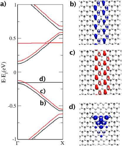
Figure 3. (a) The band structure, around the Fermi energy, for the HF defect. (b)–(d) The wavefunctions at the Γ point for the corresponding levels pointed in (a).
Download figure:
Standard image High-resolution imageFor the case of the widened and constricted nanoroads, the effect of structure change in the electronic transport is very pronounced. This can be seen in the severely attenuated transmittances (compared to pristine nanoroads) shown in figure 4. In fact, in all cases shown here the first plateau for energies above and below EF is almost entirely quenched. In all cases considered here there was no polarization of the transmission coefficients. Thus, the modification in the hybridization of few carbon atoms happens to play a big role for the electronic transport. That is a problem for electronic devices, as a small amount of misplaced hydrogen atoms can greatly disturb the electronic transport.
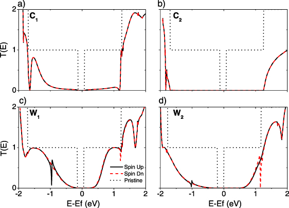
Figure 4. Spin polarized transmittances of the constrictions and widened nanoroads. (a) C1, (b) C2, (c) W1 and (d) W2.
Download figure:
Standard image High-resolution imageFinally one could point that for wider nanoroads the attenuation effects can be lowered. In order to assess that we have simulated a 15 atom wide nanoroad (17.45 Å wide), with a HE defect (ACR15HE). In figure 5 we show the transmittance plotted for the ACR15HE. It can be seen that attenuation still occurs, but especially near the Fermi energy the up and down spin channels are not evenly affected. In particular, a current polarization close to 100% is reached. Than even for wider systems the effect of a single hydrogen atom can be harmful to applications in electronic devices. Thus, on the one hand, for systems with many defects, this attenuation could be even more severe, as the conductance decays vary rapidly with the length [31]. This behavior is similar to edge disorder in graphene nanoribbons, as observed by Mucciolo et al [22]. On the other hand, if a asymmetry between up and down spin channels of the transmittance is present, polarization effects can arise and be enhanced for longer systems [32]. This kind of behavior is desired for spin filters, a important device for spintronics [33]. This effect is related to the fact that conductance and valence bands are largely dominated by the edge states.

Figure 5. Spin polarized transmittances of a 15 atom wide nanoroad (ACR15) with a HE defect.
Download figure:
Standard image High-resolution image
4. Conclusion
In summary, we have demonstrated that it is energetically favorable for hydrogen atoms to bond to nanoroads. That leads to a high suppression of the electronic transmittance, creating problems to applications in electronic devices. Even a single hydrogen can disturb the electronic transport, making it a difficult task to synthesize a clean system with single atom precision, to be useful for electronic devices. Despite the problems for electronic devices the graphane/graphene interface can be interesting to spintronics, as they show an asymmetry on the transmittance of spin up and spin down channels. This effect can be enhanced for longer systems, making the nanoroads good candidates to spin filter devices.
Acknowledgments
The authors acknowledge FAPESP and CNPq for financial support and also CCE-USP, HPC-UFABC and CENAPAD/SP for the computational time.