
Abstract
We report a simple but efficient method to fabricate versatile graphene nanonet (GNN)-devices. In this method, networks of V2O5 nanowires (NWs) were prepared in specific regions of single-layer graphene, and the graphene layer was selectively etched via a reactive ion etching method using the V2O5 NWs as a shadow mask. The process allowed us to prepare large scale patterns of GNN structures which were comprised of continuous networks of graphene nanoribbons (GNRs) with chemical functional groups on their edges. The GNN can be easily functionalized with biomolecules for fluorescent biochip applications. Furthermore, electrical channels based on GNN exhibited a rather high mobility and low noise compared with other network structures based on nanostructures such as carbon nanotubes, which was attributed to the continuous connection of nanoribbons in GNN structures. As a proof of concept, we built DNA sensors based on GNN channels and demonstrated the selective detection of DNA. Since our method allows us to prepare high-performance networks of GNRs over a large surface area, it should open up various practical biosensing applications.
Export citation and abstract BibTeX RIS
1. Introduction
Graphene is a single-atom-thick, sp2 carbon-based material that has attracted significant interest due to its remarkable electrical [1–3] and optical [4, 5] properties. Recently, extensive efforts have been devoted to develop various graphene-based devices for biological sensing applications [6–9]. However, the low transconductance of the pristine graphene hinders its application as active devices such as field effect transistor (FET) sensors [10, 11]. Furthermore, it is often very difficult to functionalize pristine graphene with chemical or biological molecules [12], and graphene layers have been reported to quench the fluorescence from dye molecules [13], making it problematic for the biological applications of graphene layers. One solution for such problems can be nanoscale ribbon structures based on graphene [10, 11, 14]. Graphene nanoribbons (GNRs) exhibited improved transconductance compared with graphene, and their edges can be functionalized with various chemical or biological molecules. GNRs have been prepared via various fabrication methods, such as e-beam lithography [10, 15], shadow mask patterning processes [16, 17], and chemical synthesis [18]. For practical device applications such as biosensors, one should be able to cover rather large size channel areas with high-quality networks of GNRs and functionalize the individual ribbons with chemical or biological molecules. However, it can be a very time-consuming and complex task to fabricate such large scale networks of GNRs via previous methods. Until now, a large scale network of GNRs has not been fabricated before, and GNR-based devices have not been utilized for practical biosensor applications.
Herein, we developed a facile method to produce graphene nanonet (GNN) patterns over a large surface area for biological applications. In this process, the networks of V2O5 nanowires (NWs) were adsorbed selectively in the desired regions on a graphene layer, and they were utilized as a shadow mask during the reactive ion etching (RIE) on the graphene layer. This fabrication process allowed us to prepare large scale patterns of GNN structures which were comprised of continuous networks of GNRs with chemical functional groups on their edges. The chemical functional groups in the GNN could be functionalized with biological molecules such as DNA for biochip applications. Significantly, GNNs were comprised of continuous networks of GNRs without any contacts between separate GNRs, which should be advantageous in achieving high-performance electrical devices with low noise and high mobility. Using the GNN-based biochip devices, we have successfully performed the fluorescence imaging of a DNA on the GNN channels and the electrical detection of the DNA at 1 nM concentrations. Our method could be a powerful strategy to mass-produce GNR-based devices and should open up various practical applications.
2. Experimental methods
2.1. Preparation of V2O5
Ammonium meta-vanadate (Aldrich, 2 mg) and acidic ion-exchange resin (DOWEX 50WX8-100, Aldrich, 20 mg) were mixed in deionized water (40 ml), and the mixture was incubated at room temperature for 20 days. During this time period, V2O5 NWs continued to grow and became over 1–10 μm long and 10–20 nm wide (figure S1 in supporting information available at stacks.iop.org/Nano/24/375302/mmedia) [19].
2.2. Fabrication of GNN-based FET device
A single-layer graphene was prepared by a chemical vapor deposition method, and it was transferred onto a SiO2 substrate (1000 Å), as reported previously (figure 1(a)) [20, 21]. Photoresist (PR, AZ5214) was patterned on a single-layer graphene surface via conventional photolithography processes (MA6 aligner, Karl Süss Company, Germany) with a short baking time (<10 min at 95 °C). Then, the V2O5 NWs were adsorbed on the graphene surface with PR patterns from its solution (figure 1(b)). Subsequently, the PR was removed by rinsing it with acetone, resulting in the V2O5 NWs adsorbed only in the bare graphene region (figure 1(c)). We etched off the sample via the RIE process (South Bay Technology Inc., 60 W, 1 min) using the V2O5 NW networks as a shadow mask (figure 1(d)). Then, the V2O5 NWs were removed via HCl solution (5%), resulting in the GNN patterns on a SiO2 surface (figure 1(e)). The HCl treatment removed only V2O5 NWs and left GNN structures (figures S2 and S3 in supporting information available at stacks.iop.org/Nano/24/375302/mmedia). The Au electrodes were prepared by photolithography followed by a thermal evaporation (ODIS, Korea) method (10 nm/30 nm of Pd/Au) under a high-vacuum condition (base pressure ∼5 × 10⁻⁶ Torr) (figure 1(f)) [22]. For biosensor devices, the metal electrodes were passivated with a PR layer. Note that this process allowed us to fabricate the patterns of continuous networks of GNRs, which can be ideal for practical device applications.

Figure 1. Schematic diagram depicting the fabrication process of a GNN-based device. (a) Transferring a single-layer graphene sheet onto a SiO2 substrate. (b) PR patterning and V2O5 NW adsorption on graphene. (c) Patterned networks of V2O5 NWs on a graphene surface after PR removal. (d) RIE for GNN patterning. Note that V2O5 NWs were utilized as a shadow mask. (e) GNN structures after the removal of V2O5 NWs via a HCl etching process. (f) Fabrication of metal electrodes for GNN-based devices.
Download figure:
Standard image High-resolution image2.3. Functionalization of GNN with DNA for the fluorescence and electrical sensing experiment
GNN patterns were incubated for 1 h in 6 mg of 1-ethyl-3-(3-dimethylaminopropyl) carbodiimidehydrochloride (EDC) and N-hydroxysuccinimide (NHS) mixed solution. Then, the edges of the GNN were functionalized with NHS molecules. Subsequently, the NHS-functionalized GNN samples were immersed in a solution of amine-terminated DNA (10 μM) with 15 bases (5'-NH2-C6-CAT TCC GAG TGT CCA) and 100 μl of 1% sodium dodecylsulfate (SDS) in 890 μl of 2-(N-morpholino) ethanesulfonic acid (MES) buffer, then incubated for 1 h at room temperature [23]. Note that these processes enabled the amide bonding between the amine group of DNA and the carboxyl group of GNN edges. The physically adsorbed DNA molecules were removed by a 1% SDS wash for 60 min. To verify the tethering of this target DNA, the GNN sample was immersed into a probe DNA (5'-cy3-TGG ACA CTC GGA ATG) terminated with cy3 dye (570 nm emission) solution for 80 min at room temperature. The nonspecifically bound DNA was removed by a 1 h wash with 1% SDS solution. For the electrical sensing experiment, the GNN-FET was exposed to the solution of an amine-terminated probe DNA (10 μM) with 15 bases (5'-NH2-C6-CAT TCC GAG TGT CCA) for 1 h, so that the amine groups in the DNA anchored to the NHS-functionalized GNN surface. Then electrical measurements and DNA sensing experiments were carried out using a Semiconductor Characterization System 4200 (Keithley Instruments Inc.).
3. Result and discussion
3.1. Analysis of GNN structure
Figure 2(a) shows the optical microscope image of line-shaped patterns comprised of GNNs on a SiO2 substrate. Note that the patterns had well-defined edges and covered a large surface area. It clearly shows that we could prepare uniform GNN patterns over a large surface area.

Figure 2. Microscopy images and XPS analysis of GNNs. (a) Optical microscope image showing large scale line patterns of GNN on a SiO2 substrate. (b) AFM topography image of GNN. (c) XPS spectrum of a bulk graphene layer. It shows only the C–C bonding peak (single fitting curve). (d) XPS spectrum of a GNN. It shows the peaks for C–O, C=O and COOH (combination of multiple fitting curves), which implies that our GNN had a large amount of functional groups on its surface. (e) Raman spectrum of a graphene layer. The G and 2D peaks were observed from the pristine graphene. (f) Raman spectrum of a GNN. The D band was observed only after the O2 plasma etching process of the graphene layer. It implies that the GNN had a large amount of disorder on its surface.
Download figure:
Standard image High-resolution imageFigure 2(b) is the atomic force microscopy (AFM) topography image of the patterned GNN on a SiO2 substrate. It shows continuous networks of GNRs with a rather uniform width. In previous works about networks of one-dimensional nanostructures such as carbon nanotubes (CNTs), the contact resistance between individual nanostructures often caused significant problems, such as low mobility and high noise in the device channels. In our case, GNN is comprised of continuous networks of GNRs without contact resistances, which can be a significant advantage in achieving high-performance devices.
Figures 2(c) and (d) show the x-ray photoelectron spectroscopy (XPS) spectra of the bulk graphene layer and GNN, respectively. The bulk graphene layer exhibited only a single peak associated with the sp2 carbon bonds (red curve at 284.8 eV). On the other hand, the GNN had peaks associated with oxygen, hydroxyl groups and carboxylic groups as well as C–C bonds (combination of multiple fitting curves). Note that the oxygen-containing groups were attached to the broken carbon bonds on the GNN, which was caused by the RIE process. This implies that the GNN had many functional groups such as OH and COOH at its edge regions [14], which should allow us to chemically functionalize the GNN for various applications [24].
Figures 2(e) and (f) show the Raman spectra of the bulk graphene layer and GNN, respectively. The bulk graphene layer had only G and 2D bands (figure 2(e)), while the GNN had an additional D band (figure 2(f)). Here, the presence of the defect-related D band was attributed to the broken carbon bonds of the GNN [25]. This result confirms that a number of chemically reactive groups existed in our GNNs.
3.2. Functionalization of a DNA on the GNN template and fluorescence imaging
Figure 3(a) shows schematic diagrams depicting the procedure for the functionalization of a DNA on the GNN for optical biochip applications. GNN patterns were expected to have a number of carboxylic groups due to the edges of GNRs it contained (figure 3(a)(i)). These carboxylic groups could be utilized to link with amine-terminated probe DNA via amide bonding after an activation process with NHS/EDC (figure 3(a)(ii)) [26]. Then, the fluorescent DNA probe terminated with cy3 dye was utilized to verify the DNA functionalization of the GNN (figure 3(a)(iii)).

Figure 3. Functionalization of GNN patterns with DNA for optical biochip applications. (a) Schematic diagram depicting the functionalization and hybridization of DNA on GNN patterns. (i) GNN patterns with carboxyl groups on their surface. (ii) Functionalization of the GNN patterns with probe DNA. The amine-terminated DNA molecules were linked to the carboxylic groups on the GNN surface via amide bonding after an activation process with NHS/EDC. (iii) Hybridization with dye-labeled DNA (target DNA). (b) Optical microscopy image of GNN patterns over a large surface area on a SiO2 substrate. The area in the dashed square indicates one of the GNN patterns. (c) Fluorescence image of GNN patterns after the hybridization with dye-labeled DNA (as shown in (a)(iii)) and (d) its profile. It confirms that our GNN can be functionalized with biomolecules such as DNA, and it can be utilized with fluorescence molecules without a significant quenching problem.
Download figure:
Standard image High-resolution imageFigure 3(b) shows the optical microscopy image of GNN patterns over a large surface area on a SiO2 substrate. Note that it shows uniform patterns with well-defined edges. Figures 3(c) and (d) show the fluorescence image and its intensity profile of the cy3-DNA-hybridized GNN patterns, respectively. The fluorescent image clearly shows that the cy3-DNA was selectively attached only on the GNN which was functionalized with amine-terminated DNA. The intensity profile of figure 3(d) confirms that a uniform layer of cy3-DNA was formed after the hybridization. These results clearly show that our GNN can be selectively functionalized with biomolecules, and it can be labeled with fluorescence molecules for fluorescence-based biochip applications.
For the control experiment, the amine-terminated DNA attached on GNN was hybridized with non-complementary DNA (5'-cy3-GAT CTG AGT ATC CGT). In contrast to figure 3(c), no significant fluorescence signal was observed (figure S4(a) in supporting information available at stacks.iop.org/Nano/24/375302/mmedia). Furthermore, the nonspecific binding of the cy3-DNAs onto the GNN pattern was not observed either (figure S4(b) in supporting information available at stacks.iop.org/Nano/24/375302/mmedia).
3.3. Electrical characteristics and sensor applications of GNN
Figure 4(a) shows the Ids–Vg curves of the bulk graphene layer-based FET (a blue line) and the GNN-based FET (a red line). The length and width of the GNN channel were 10 μm and 2 μm, respectively (figure S5 in supporting information available at stacks.iop.org/Nano/24/375302/mmedia). For the current measurement, the bias voltage of 1 V was applied to the GNN-FETs. The bulk graphene-FET exhibited typical ambipolar characteristics, while the GNN-FET exhibited p-type characteristics (figure 4(a) and figure S6 in supporting information available at stacks.iop.org/Nano/24/375302/mmedia). The p-type characteristics of GNN-FET were attributed to oxygen edge groups which were generated by the RIE process [27]. It should be noted that the FET device based on our networks of GNRs exhibited a rather high mobility (∼100 cm2 V−1 s−1) compared to that based on CNT networks [28]. Presumably, the nanoribbons in our GNN were connected continuously without any high-resistance contact points between individual nanoribbons, which should have helped in reducing the scattering of charge carriers and enhancing its mobility. Such high mobility should be advantageous in building high-performance devices based on GNN, such as FETs and sensors.

Figure 4. Electrical characterization of GNN channels and its application for electrical DNA sensing. (a) Gating effect of a FET device based on a bulk graphene layer (a blue line) and a GNN channel (a red line). The GNN channel exhibited p-type characteristics with a rather high transconductance compared with the bulk graphene layer. (b) Normalized power spectral density S/I2 of current noise from the GNN channel as a function of a frequency f. Note that the normalized power spectral density was proportional to the inverse of the frequency, indicating a typical 1/f noise behavior. (c) A real-time current measurement obtained from a GNN-based DNA sensor after the introduction of complementary (red) or non-complementary (green and blue) DNA at various concentrations. The non-complementary DNA 1 had only a single base mismatch compared with complementary DNA. (d) Conductance changes of the GNN-FET by the introduction of various concentrations of complementary DNA solutions. The red line represents the fitting curve for the estimation of the dissociation constant (Kd).
Download figure:
Standard image High-resolution image
Figure 4(b) shows the current-normalized power spectral density (PSD) S/I2 as a function of the frequency f. The noise measurement was performed using a FFT network analyzer (SR770, Stanford Research Systems) with a source–drain bias voltage of 1 V on the GNN-FET. The PSD was found to be inversely proportional to the frequency f, which is a typical low-frequency noise behavior of graphene-based devices [29, 30]. Note that the noise level of the GNN-FET was similar to that of bulk graphene-based devices (S/I2 < 10−8 Hz−1) [29, 30] and lower than that of CNT network-based devices (S/I2 < 10−5 Hz−1) [31]. Furthermore, the noise amplitude normalized by a resistance value (A/R) of the GNN-FET was ∼6.46 × 10⁻¹² Ω−1, which was lower than that of CNT network-based devices [31] and was similar to that of the pristine single-layer graphene-based devices [29, 30]. In previous works, the network-based devices were usually comprised of separate nanostructures such as CNTs or NWs, where the contact resistance between individual nanostructures can cause a significant noise and resistance in the device [32]. In contrast, our GNN is comprised of continuous networks of GNRs, which should have reduced possible noise sources in the channel. Such low noise characteristics of our GNN should be an important advantage for high-precision devices such as highly sensitive sensors.
As a proof of concept, we functionalized GNN with DNA and built DNA sensors. Figure 4(c) shows the real-time detection of complementary DNA (5'-TGG ACA CTC GGA ATG-3') at various concentrations from 10 pM to 1 μM. In this experiment, the GNN channel in a GNN-FET was first functionalized with DNA. Then, a 100 mV bias voltage was applied between the source and drain electrodes, and the source–drain current was monitored after the addition of the target DNA with different concentrations. The red, blue and green lines are the responses of our sensor to the addition of the complementary, non-complementary DNA 1 (5'-TGG AGA CTC GGA ATG-3') and non-complementary DNA 2 (5'-GAT CTG AGT ATC CGT-3'), respectively. Note that the non-complementary DNA 1 had only a single mismatched base compared with the complementary DNA. The addition of the complementary DNA with its concentration over 1 nM resulted in significant current changes, while the sensor did not respond to the non-complementary DNA. This conductance decrease by the complementary DNA could be explained by the electron-doping of the negatively charged DNA on the GNN channel [33]. Our results show that the GNN structures can be functionalized with biomolecules and utilized to build biosensors for the selective detection of biomolecules such as DNA. Also, the limit of detection is comparable or even lower than previous graphene-based electrical sensors for DNA detection [6, 9, 34].
Figure 4(d) shows the response curve of our DNA sensor based on GNN. This sensor response could be fitted by the typical response equation of FET-type sensors, as reported previously [35–38]:
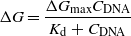
where ΔGmax and CDNA are the saturated net change in conductance and the concentration of complimentary DNA in solution, respectively. The term Kd represents the dissociation constant between target and probe DNA molecules. Note that the sensor response curve is fitted well to this theoretical fitting curve (red line). The fitting allowed us to estimate the dissociation constant Kd as 1.4 × 10⁻¹⁰ M, which is similar to the previous reported value measured by other methods [39, 40].
4. Conclusion
In conclusion, we developed a method to produce GNN patterns over a large surface area for biological applications. In our method, the networks of V2O5 NWs were patterned selectively in the desired regions on a graphene layer, and they were utilized as a shadow mask during the RIE process. Our fabrication processes allowed us to prepare large scale patterns of GNN structures which were comprised of continuous networks of GNRs with chemical functional groups on their edges. The chemical functional groups in the GNN could be functionalized with biological molecules such as DNA for biochip applications. Significantly, since GNNs were comprised of continuous networks of GNRs, FET devices based on GNN channels exhibited a low noise as well as a high mobility. Using the GNN devices, we could successfully perform the fluorescence imaging of a DNA on the GNN and the electrical detection of the DNA at 1 nM concentrations. Our method could be a powerful strategy to mass-produce GNR-based devices and should open up various practical applications.
Acknowledgments
This work was supported by the NRF grant (Nos 2013003416, NRF-2013R1A1A2012434, 2009-0083540) and the WCU program (R31-10032). SH acknowledges financial support from the Pioneer Research Center Program through the National Research Foundation (No. 2013007874) and the Conversing Research Center Program through the Ministry of Science, ICT and Future Planning, Korea (2013K000369). THK acknowledges financial support from Leaders Industry–University Cooperation Project, supported by the Ministry of Education, Science & Technology (MEST).