
Abstract
With the aim of preparing paper-based writing electronics, a kind of conductive pen was made with nano-silver ink as the conductive component and a rollerball pen as the writing implement. This was used to direct-write conductive patterns on Epson photo paper. In order to decrease the sintering temperature, pressure was introduced to enhance the driving forces for sintering. Compared with hot sintering without pressure, hot-pressure can effectively improve the conductivity of silver coatings, reduce the sintering time and thus improve productivity. Importantly, pressure can achieve a more uniform and denser microstructure, which increases the connection strength of the silver coating. At the optimum hot-pressure condition (sintering temperature 120 ° C/sintering pressure 25 MPa/sintering time 15 min), a typical measured resistivity value was 1.43 × 10⁻⁷ Ω m, nine greater than that of bulk silver. This heat treatment process is compatible with paper and does not cause any damage to the paper substrates. Even after several thousand bending cycles, the resistivity values of writing tracks by hot-pressure sintering stay almost the same (from 1.43 × 10⁻⁷ to 1.57 × 10⁻⁷ Ω m). The stability and flexibility of the writing circuits are good, which demonstrates the promising future of writing electronics.
Export citation and abstract BibTeX RIS
1. Introduction
With the development of lightweight and flexible electronic products, traditional rigid printed circuit boards cannot meet the requirements of current electronic components [1–3]. Recent efforts have focused on the design of conductive inks for integration on plastic [4], textile [5] and paper substrates [6] for flexible electronics. As a substrate for fabricating flexible electronics, paper could potentially cause a breakthrough in the electronics world. Paper-based electronics are lightweight, biodegradable and recyclable, and can also be rolled or folded into three-dimensional (3D) flexible configurations (see figure 1) [7]. To demonstrate the device fabrication capabilities, Lewis et al [7] produced electronic art, multi-color LED displays and 3D antennas on paper substrates for the first time: an electronic sketch of the famous painting 'Sae-Han-Do' was drawn using silver ink. Because the whole circuit is made of paper and silver ink it will naturally biodegrade after use and does not pose a threat to the environment. Hence, it has broad prospects for application in electronics. More importantly, a modified rollerball pen loaded with conductive ink or semiconductive and dielectric ink can directly write electronic text and patterns on paper to achieve paper-based writing electronics. Compared with other functional printing approaches, such as screen printing and inkjet printing, this direct-writing method is more portable for a paper substrate.
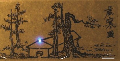
Figure 1. Optical image of conductive electronic art drawn with a silver-ink filled rollerball pen on Xerox paper.
Download figure:
Standard image High-resolution imageTo date, conductive polymer [8], carbon nanotube (CNT) [9] and graphene [10] inks have been demonstrated. However, organic inks typically exhibit low conductivity, poor chemical and thermal stability whereas carbon-based inks are generally not widely used for low resistivity material because of poor conductivity [11, 12]. Recent exploration into metallic nanoparticle inks has yielded promising results. Since silver is the best conductor (especially since the oxide is also conductive), silver nanoparticle inks have been the most popular conductive inks used in functional printing [13].
For silver nanoinks, an additional sintering processing step is necessary to form a conductive pattern. Simple application of heat is the most commonly used sintering process and usually requires temperatures above 200 ° C or requiring times exceeding 60 min [9, 14]. However, the high sintering temperatures limit the application of silver nanoinks on flexible paper substrates and the long sintering time limits the productivity. Thus, it would be useful to reduce both the temperature and time required for sintering, and this is the focus of research. To date, many studies have been conducted to reduce the sintering conditions to room temperature. Smith et al [15] reported that an inkjet printed or spincoated silver neodecanoate solution can be activated by light and subsequently treated with a chemical agent to produce conductive silver at room temperature. However, the process is time consuming and the resistivity (1.54 × 10⁻⁷ Ω m) is about 10 times that of bulk silver. Magdassi et al [16] reported that Cl ions cause detachment of the anchoring groups of the stabilizer from the nanoparticle surfaces, thus enabling their coalescence and sintering at room temperature. Finally, up to 2.44 times the resistivity (3.84 × 10⁻⁸ Ω m) of bulk silver was achieved. However, Cl ions in the wet solution (HCl) will contaminate the paper-based substrate.
Over the last few years more selective sintering techniques, including laser sintering [17], microwave sintering [18], UV radiation [19] and high temperature plasma sintering [20], have been used to sinter printed nanoparticle structures. These sintering methods are rapid and selective, and do not harm the thermo-sensitive substrates. However, most of them are costly and complex to operate. Thus, a fast, simple and cost-effective sintering technique is urgently needed.
Hot pressing sintering is widely used in powder metallurgy. Based on the science of sintering, pressure could speed up the sintering kinetics for densification of a particle compact. To realize low-temperature rapid sintering, mechanical pressing at lower temperature is an effective, proven method. The purpose of pressure is twofold. Firstly, the pressure increases the contact area/number of contact points between silver nanoparticles (Ag NPs). Secondly, the pressure helps to give a more uniform and denser microstructure. Meanwhile, pressure does not damage to the substrates because of the suppleness of paper. The results of a literature search indicate that no study has been conducted on the use of a mechanical pressing method to reduce the sintering temperature and time for printed electronics/writing electronics, in particular Ag NP conductive ink on a paper substrate.
Therefore, in the present study, Ag NPs covered by surfactant were synthesized in an aqueous solution by reducing silver nitrate (AgNO3) with sodium borohydride (NaBH4) in the presence of poly(vinyl pyrrolidone) (PVP) as a stabilizer. Then, a kind of conductive pen was designed, prepared with nano-silver ink as the conductive component and a rollerball pen as the writing implement, and used to direct-write conductive patterns on Epson photo paper. Hot-pressure was applied to convert the non-conductive direct patterns into their conductive counterparts. The conductivity, mechanical flexibility and adhesion characteristics of the hot-pressure sintering patterns were also studied.
2. Experimental details
2.1. Materials
Silver nitrate (AgNO3, 99%), PVP (MW 10 000 g mol−1), sodiumborohydride (NaBH4), glycerol, ethylene glycol and absolute ethyl alcohol were purchased from Tianjin Jiangtian Chemical Co. Ltd and used without additional purification.
2.2. Nano-silver ink preparation
Ag NPs were synthesized in an aqueous solution by reducing silver nitrate in the presence of a surface capping agent, PVP. In a previous published synthesis of Ag NPs [21], briefly, 1.5 g of AgNO3 and 1.0 g of PVP were dissolved in 200 ml of deionized water under vigorous stirring. Next, 20 ml of prepared NaBH4 solution (20 mg ml−1) was added dropwise to the stirring reaction mixture, the process continuing for 10 min. The color of the solution changed nearly instantly from transparent to dark yellow. The reaction was kept for another 10 min after dropping the NaBH4 and was then centrifuged at a speed of 8000 rpm for 20 min. The precipitate was then redispersed in 30 ml of glycerol by sonication. The resulting solution was centrifuged again at 8000 rpm for 20 min to remove excess PVP. The precipitate (Ag NPs) was collected and dried in air for further studies.
For the preparation of the nano-silver conductive ink, the obtained Ag NPs were dispersed in ethanol, and ethylene glycol and glycerol were added to adjust the writability of the ink. The solvent composition of compounded ink was ethanol:ethylene glycol:glycerol =50:45:5 vol.%. The solid loading of Ag NPs for hybrid ink was 20 wt%. Tracks can be easily drawn with this kind of conductive pen on Epson photo paper, just like writing on ordinary paper, with the same speed and force.
2.3. Conductive pen setup
M&G rollerball pens with ball diameters of 0.38, 0.5, 0.7, 1.0 mm were used in the present study. Firstly, the original ink was removed with running water. Secondly, the ink barrel and rollerball tip were cleaned thoroughly in ethanol in an ultrasonic bath. Finally, the prepared hybrid ink was injected into the cartridge by micro-syringe. With different ball diameters, we could achieve widths of written electrodes ranging from 300 μm to 1 mm or higher, as shown in figures 2(a) and (b).

Figure 2. (a) Optical image of rollerball pen refills; ball diameters are 0.38, 0.5, 0.7, 1.0 mm respectively from left to right respectively. (b) Optical image of written lines of different widths by different ball diameters.
Download figure:
Standard image High-resolution image2.4. Hot pressing sintering
The hot pressing sintering device used in this study is the Carver manual pressing machine, as shown in figure 3. The platen size is 38.1 cm × 38.1 cm. The upper and lower heating sides can work at the same time. The heating temperature is adjusted by the programmable table and the maximum heating temperature is 343 ° C. The maximum pressure is up to 75 kN. During the test, the lower plate is fixed and the upper plate is moved by four mobile screws, thus ensuring parallelism between the two plates. The pressure is applied by the manual hydraulic control and displayed via digital presses. During the test, the upper and lower surfaces of the circuit in the paper are covered by polyimide film to prevent the contamination of the sample by the heating plate.
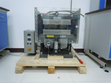
Figure 3. Device for hot pressing sintering.
Download figure:
Standard image High-resolution image2.5. Instrumentation
The surface morphology and structure of Ag NPs were characterized by transmission electron microscopy (TEM; Philips Tecnai G2 F20). The direct-writing tracks on paper were examined by field emission scanning electron microscopy (FE-SEM; Hitachi S-4800). A four-probe method was used to measure the resistance of the drawn electric circuits.
3. Results and discussions
3.1. The characters of the silver conductive ink
Central to the conductive pens is the design of a silver ink that readily flows through the pen tip during writing, and does not leak, dry out or coagulate within the pen. To create an ink with these attributes, we synthesized Ag NPs in an aqueous solution by reducing silver nitrate in the presence of a surface capping agent, PVP. As shown in figure 4, Ag NPs with an average size of 40 nm were obtained. The XRD results are in agreement with the literature values for face centered cubic (fcc) silver crystals, as shown in figure 5. The prominent peaks at respective 2θ values known for zero-valent fcc silver representing the (111), (200), (220) and (311) crystal planes due to Bragg reflections are present. The PVP stabilizer plays an important role in the preparation of aqueous Ag NP ink. The reaction without PVP resulted in formation of an insoluble powder. Importantly, PVP binds weakly to the Ag NP surfaces, compared with thiols and primary amines [22]. The weakly adsorbed PVP can desorb readily from the surfaces of the NPs and collapse after solvent evaporation.
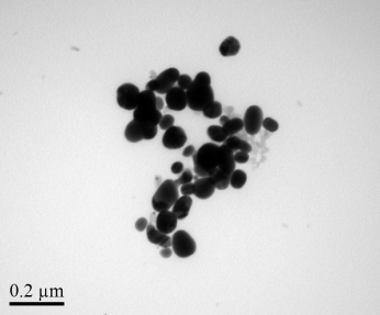
Figure 4. TEM image of synthesized Ag nanoparticles.
Download figure:
Standard image High-resolution image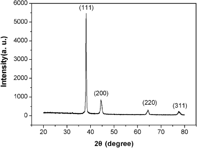
Figure 5. XRD patterns of synthesized Ag nanoparticles.
Download figure:
Standard image High-resolution imageEthylene glycol and glycerol are two common additional agents for commercial ink applied in rollerball pens which can effectively improve the viscosity, surface tension and wettability of the ink, thus increasing the writing quality. To create an ink with good writability, we use ethylene glycol and glycerol to improve the flow properties of the ink. The optimized ratio of the solvent is ethanol:ethylene glycol:glycerol =50:45:5 vol.%. Under this circumstance, ink could readily flow through the pen tip during writing, and didn't leak or clog.
3.2. The role of pressure
To lower the sintering temperature, we explored a strategy of using mechanical force to enhance the driving forces for sintering. To demonstrate the role of pressure, we produced a linear array of five silver tracks (width =∼ 0.8 mm,height =∼ 2.5 μm, and length= 60 mm) using a 1.0 mm roller ball pen filled with nano-silver ink (20 wt% silver) on Epson photo paper and dried at room temperature for 2 h in air. Then one set of silver tracks was sintered at 120 ° C for 60 min, and another set of silver tracks was sintered at 120 ° C and 25 MPa for 15 min.
Figure 6(a) shows the average electrical resistivity of the silver track array by direct writing after drying under ambient conditions (25 ° C) and as a function of hot sintering time. The electrical resistivity of the silver tracks decreases with increasing hot sintering time. After hot sintering at 120 ° C for 60 min, the resistivity of the nano-silver ink goes to nearly 9.2 × 10⁻⁷ Ω m. Figure 6(b) shows the average electrical resistivity of the silver track array by direct writing after drying under ambient conditions (25 ° C) and as a function of hot-pressure sintering time. After hot-pressure at 120 ° C and 25 MPa for 15 min, the resistivity reduces to 1.8 × 10⁻⁷ Ω m. The electrical resistivity of silver tracks for both hot-pressure sintering and hot sintering first decreased with increasing sintering time and then stayed the same after all the solvent had evaporated. After sintering, the electrical resistivity of silver tracks by hot sintering (∼9.2 × 10⁻⁷ Ω m) is nearly five times higher than that of silver tracks by hot-pressure sintering (∼1.8 × 10⁻⁷ Ω m). Meanwhile, the hot sintering time (∼60 min) is four times longer than the hot-pressure sintering time (∼15 min). Therefore, hot-pressure can effectively improve the electrical performance of written silver tracks and enhance productivity.
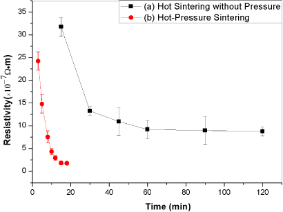
Figure 6. (a) Electrical resistivity as a function of hot sintering time (temperature 120 ° C, pressure 0). (b) Electrical resistivity as a function of hot-pressure sintering time (temperature 120 ° C, pressure 25 MPa).
Download figure:
Standard image High-resolution imageTo further demonstrate the role of pressure, we observe the difference in morphology of the written coating for different sintering conditions. Figure 7(a) shows the surface morphology of the written coating by drying at room temperature for 2 h in air. The NPs are point contact based and there is no obvious sintering phenomenon between NPs. Figure 7(b) shows the surface morphology of the written silver tracks after drying at room temperature for 2 h in air and sintering at 120 ° C for 1 h. With the action of driving forces for sintering, grain boundary diffusion allows for neck formation, the contacts between NPs change from point contacts to surface contacts. Figure 7(c) shows the surface morphology of the written coating by drying at room temperature for 2 h in air and sintering at 120 ° C and 25 MPa for 15 min. Compared with hot sintering, the neck radii between NPS by hot-pressure sintering increase, which demonstrates that pressure could enhance the sintering driving forces. Figures 8(a) and (b) show the cross-sectional morphology of the written coating by hot sintering and hot-pressure sintering. The sintering phenomenon between NPs by hot-pressure sintering is more obvious than that of hot sintering along the cross-section direction. The difference in the morphology of the written coating demonstrates that hot-pressure can effectively improve the conductivity of the written coating.

Figure 7. Surface SEM image of the silver tracks on Epson photo paper for different sintering conditions: (a) by drying at room temperature for 2 h in air, (b) by drying at room temperature for 2 h in air, then sintering at 120 ° C for 1 h, and (c) by drying at room temperature for 2 h in air, then sintering at 120 ° C and 25 MPa for 15 min.
Download figure:
Standard image High-resolution image
Figure 8. Cross-sectional SEM image of the silver tracks on Epson photo paper for different sintering conditions: (a) by hot sintering (temperature 120 ° C, sintering time 60 min) and (b) by hot-pressure sintering (temperature 120 ° C, pressure 25 MPa, sintering time 15 min).
Download figure:
Standard image High-resolution image3.3. The electrical properties of paper-based electronics
Paper, as a substrate for fabricating flexible electronics, offers a set of unique performance characteristics. However, different paper types have an important influence on the conductivity of written films. For common printing paper, it was observed that the written patterns have a poor conductivity. The reason may be the rough surface of common printing paper which prevents the continuity of the conductive films. For smooth photo paper there is a coating of silicon dioxide NPs, which forms tiny inorganic–organic hybrid fine particles. These micro-porous papers cannot only absorb solvent and residual PVP molecules rapidly, but also enhance the adhesion strength of the conductive film. Low adhesion strength always results in adhesion failure. In the present study, a tape test was employed to test the adhesion force of the coating. The test procedures is as follows: put tape on the surface of the printed width of a coating then remove the tape along a certain angle. How/if the coating peels off determines the effect of adhesion. The tape test demonstrates the good adhesion between paper substrates and written films.
The paper substrates used in flexible electronics are usually heat-sensitive. When the sintering temperature exceeds 150 ° C, we found that photo papers become crisp, which seriously affects their use in flexible electronics. Hence, we make the sintering temperature 120 ° C. There is no effect on the paper substrate when forcing because of the good malleability of paper. Figure 9 shows the electrical resistivity as a function of pressure under a sintering temperature 120 ° C and sintering time of 5 min. It can be observed that the optimal sintering pressure is 25 MPa.

Figure 9. Electrical resistivity as a function of sintering pressure (temperature 120 ° C and sintering time 5 min).
Download figure:
Standard image High-resolution imageAt the optimal hot-pressure condition (sintering temperature 120 ° C, sintering pressure 25 MPa and sintering time 15 min), the electrical resistivity ρ of the hybrid ink is calculated with the traditional method, that is

where R is the resistance, l is length and A is the cross-sectional area of the line. The thickness of conductive films can be measured accurately through the cross-section morphology of the written coating. The length and width of the silver tracks were measured using a spiral micro-distance measuring method. So

where R = 4.3 Ω,b = 0.8 mm,t = 2.5 μm,l = 60 mm. A typical resistivity value measured for this sample is 1.43 × 10⁻⁷ Ω m, which is nine times the value for bulk silver.
3.4. The mechanical properties of paper-based electronics
To demonstrate the mechanical flexibility of the silver tracks produced by direct writing and hot-pressure sintering, we measured the change in electrical resistivity before and after bending cycles. The silver tracks (width =∼ 800 μm,height =∼ 2.5 μm, and length= 6 cm) were drawn by rollerball pen (ball diameter= 1.0 mm) on Epson photo paper. The bending angle was kept around 90° (see figure 10) for 1000 bending cycles, and the resistivity values were recorded at 100, 200, 300, 400, 500, 600, 700, 800, 900 and 1000 cycles. Figure 11 shows the electrical resistivity of the silver tracks as a function of bending cycles and sintering conditions. Under hot sintering conditions (sintering temperature 120 ° C, sintering time 60 min), the resistivity of the silver tracks clearly increases after 1000 cycles. For hot-pressure sintering conditions (sintering temperature 120 ° C, sintering pressure 25 MPa, sintering time 15 min), the resistivity changes insignificantly over 1000 cycles, which indicates that pressure increases the connection strength of the written coating.

Figure 10. Photograph of a written pattern on a paper substrate bent outwards by nearly 90° hot sintering (120 ° C for 60 min) and hot-pressure sintering (120 ° C and 25 MPa for 15 min).
Download figure:
Standard image High-resolution image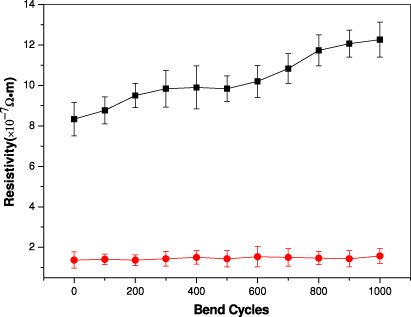
Figure 11. Electrical resistivity of the silver tracks as a function of bending cycles and sintering conditions: hot sintering (120 ° C for 60 min) or hot-pressure sintering (120 ° C and 25 MPa for 15 min).
Download figure:
Standard image High-resolution imageTo support this view, we observe the different morphologies of the written coating before and after bending. Figures 12(a) and (b) show the morphologies of the silver tracks by hot sintering without pressure. Before bending, the silver coatings are arranged loosely and a lot of pore spaces exist. After bending, the phenomenon of fracture tearing occurs. Figures 13(a) and (b) show the morphologies of the silver tracks by hot-pressure before and after bending. Before bending, the silver coatings are compact and uniform. The surface of the coatings is smooth. After bending, the silver coatings almost stay constant. The pressure helps in gaining a more uniform and denser microstructure, which increase the connection strength of written coating.

Figure 12. SEM image of the silver tracks by hot sintering (120 ° C for 60 min) before (a) and after (b) bending.
Download figure:
Standard image High-resolution image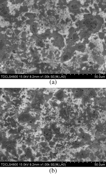
Figure 13. SEM image of the silver tracks by hot-pressure sintering (120 ° C and 25 MPa for 15 min) before (a) and after (b) bending.
Download figure:
Standard image High-resolution image3.5. Application
To demonstrate the application of nano-silver conductive ink for writing electronics, we fabricated a simple electronic circuit on paper, as shown in figure 14. The circuit is composed of a 3.0 V battery, a written pattern and a surface-mount LED with a rated voltage of 3.0 V. The conductive tracks were drawn by rollerball pens (ball diameter= 1.0 mm) on Epson photo paper and sintered at 120 ° C and 25 MPa for 15 min. The surface-mounted LED was placed in a gap between the written conductive tracks. When the circuit is on, the LED is illuminated, and works rather well. With the driving of a 3.0 V power supply, the 3.0 V LED can work normally and circuit loss is very low, which demonstrates that our conductive tracks prepared by direct writing using nano-silver ink have a fairly low resistivity. This indicates that Ag NP ink by direct writing and hot-pressure can be used to fabricate complicated conductive patterns with high conductivity and flexibility on paper substrates.

Figure 14. Optical image of an electrical circuit drawn by a rollerball pen (1.0 mm ball diameter) on Epson photo paper. The inset is the off state of the LED.
Download figure:
Standard image High-resolution image
4. Conclusions
In conclusion, the synthesized Ag NPs adsorbed by a small amount of PVP were dispersed in ethanol, and ethylene glycol and glycerol were added to adjust the writability of the ink. The solid loading of Ag NPs for ink was 20 wt%. A kind of conductive pen was designed, prepared with nano-silver ink as the conductive component and a rollerball pen as the writing implement, and used to direct-write conductive patterns on Epson photo paper. Hot sintering and hot-pressure sintering were adopted to make the direct-writing patterns conductive. Compared with hot sintering, hot-pressure sintering decreased the sintering time and reduced the resistivity of the direct-writing coating. A typical resistivity value measured was 1.43 × 10⁻⁷ Ω m, nine times greater than bulk silver. A series of test results showed that the paper-based circuit by direct-writing and hot-pressure sintering had good stability and mechanical flexibility. Based on these excellent properties, a simple paper-based electrical circuit has been fabricated to demonstrate the use of this ink for writing electronics.
Acknowledgments
The authors acknowledge the research funding by National Natural Science Foundation of China (grant no. 51205282), Research Fund for the Doctoral Program of Higher Education of China (grant no. 20120032120019), Program for New Century Excellent Talents in University (grant no. NCET-11-0375) and Key Project in the Science and Technology Pillar Program of Tianjin (grant no. 11ZCKFGX03000).