
Abstract
The development of simple gas sensing concepts is still of great interest for science and technology. The demands on an ideal device would be a single-step fabrication method providing a device which is sensitive, analyte-selective, quantitative, and reversible without special operating/reformation conditions such as high temperatures or special environments. In this study we demonstrate a new gas sensing concept based on a nanosized PtC metal-matrix system fabricated in a single step via focused electron beam induced deposition (FEBID). The sensors react selectively on polar H2O molecules quantitatively and reversibly without any special reformation conditions after detection events, whereas non-polar species (O2, CO2, N2) produce no response. The key elements are isolated Pt nanograins (2–3 nm) which are embedded in a dielectric carbon matrix. The electrical transport in such materials is based on tunneling effects in the correlated variable range hopping regime, where the dielectric carbon matrix screens the electric field between the particles, which governs the final conductivity. The specific change of these dielectric properties by the physisorption of polar gas molecules (H2O) can change the tunneling probability and thus the overall conductivity, allowing their application as a simple and straightforward sensing concept.
Export citation and abstract BibTeX RIS
1. Introduction
In the past few years selective gas detection with both a qualitative and quantitative character has attracted enormous attention due to its many possible applications (automotive sensors, environmental monitoring, industrial emission control, etc) [1–3]. Beside the demands for low detection limits, gas selectivity, reversibility, robustness, and long-term stability, particular importance is given to a simple fabrication method, compact dimensions and uncomplicated operation conditions, such as room temperature production or the absence of special conditioning steps for reformation after gas detection [1–3]. Many different material and device concepts have been demonstrated, ranging from thin-film polymers [4], metal nanoparticles and carbon nanotubes to semiconducting oxides [5], which still have considerable impact to date [6]. Humidity sensors represent a special class of devices, as they are used for a diverse range of applications, ranging from simple ambient monitoring over process control systems for industrial applications to highly sensitive reference systems for sensor arrays, for example, to eliminate cross-influences [7, 8]. Within this class, different concepts have been demonstrated, such as optical, mass sensitive, resistive or capacitive based detection [4]. The latter is the most commonly used principle which uses a polymer as a dielectric transducer material. Such polymer concepts are mostly based on material swelling or a change in the dielectric constant during water absorption [4, 9]. In both cases the capacitance changes with the environmental humidity, which can then be detected directly or, for example, be embedded as a variable gate dielectric. Despite their excellent performance, most of these concepts have drawbacks, such as time-consuming and cost-intensive fabrication methods (resist based multi-steps), partly complicated activation/reformation conditions (as necessary for metal oxides, metal nanoparticles, or carbon nanotubes) or harsh operation conditions such as very high temperatures (e.g. metal oxides, metal nanoparticles) [1–4]. Capacitive H2O sensors are easier to handle with respect to activation/reformation conditions and provide short response times in the sub-minute range [9, 10]. Although fast preparation concepts, such as ink-jet printing of the active polymer layer [11], have been demonstrated, many small size H2O sensors require time-consuming and cost-intensive preliminary steps due to their multilayer architectures [9]. As an alternative, we present a new sensor concept which uses direct write focused electron beam induced deposition [12–14] (FEBID) from a gaseous Pt based MeCpPt(IV)Me3 precursor [15], without requiring any pre- or post-treatment of the sample, that even allows fabrication on non-flat surfaces with spatial nanometer resolution [12, 13, 16]. Such Pt based devices have been successfully demonstrated to act as fully reversible stress–strain sensors as a result of variable conductivity based on the nanogranular structure of metal particles embedded in an insulating carbon matrix [14, 17–19]. The presented gas nanosensors reveal a quantitative selectivity to H2O in ambient conditions as well as reversibility without special reformation conditions and a negligible temperature influence, which is highly desirable for this type of application. The study is completed by a theoretical model and related calculations of the underlying effect, showing good agreement with the experimental results.
2. Results and discussion
After fabrication in a scanning electron microscope, the devices were exposed to ambient conditions (19 °C, 45% humidity) and subjected to a basic electrical characterization. Figure 1(a) shows the results of long-time current measurements at a fixed bias voltage for different layer thicknesses, normalized to the initial resistance. Generally, the devices revealed a decaying and saturating tendency, a behavior which is known for FEBID structures [20, 21]. Clearly, decreasing layer thicknesses result in a faster decay and saturation. For 5 and 10 nm devices, saturation current values of 2 (±0.5)% from the initial values have been found. The origin of this effect is not completely understood, but is attributed to chemical processes as a consequence of the dissociation process in FEBID and the formation of unsaturated/radical fragments such as cyclopentadiene deprotonation or the dimerization of two cyclopentadiene rings [12, 22, 23]. This might result in different properties of the insulating matrix between the Pt grains, thus changing the conductivity of the deposit [14, 24–26]. Transmission electron microscopy (TEM) investigations of such thin films revealed the typical appearance of Pt grains with diameters between 2 and 3 nm, embedded in a hydrocarbon matrix [6, 9, 12]. Cross sectional analyses of as-prepared films via STEM and complementary AFM measurements suggest a compact morphology as long as they are not exposed to post-growth e-beam curing where surface nanoporosity can occur [18, 27]. Self-driven grain growth has never been observed in such films and can therefore be excluded as the origin of the self-driven conductivity variations [17, 18]. The fact that thinner deposits (with the same deposit footprint) reach their saturation much faster permits the assumption that the surface is involved in this effect, for example, via outward diffusion of volatile products or inward diffusion of ambient components and subsequent chemical reactions within the layer. Complementary I/U curves of self-cured devices (figure 1(b)) revealed a fully linear behavior between ±1 V even for very thin devices (inset top left) and a resistivity range of 107–1010 μΩ cm (inset bottom right), which is typical for focused electron beam induced PtC deposits [12, 15, 17, 18]. The strong resistivity increase for very thin layers can be explained by the transition from a 3D bulk towards a quasi-2D granular monolayer in accordance with the Pt grain diameter of 2–3 nm.
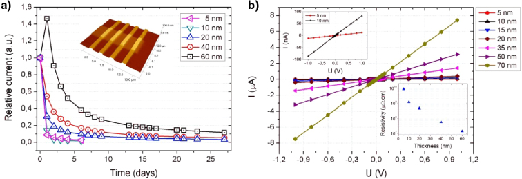
Figure 1. (a) Electrical current at a fixed bias voltage of 1 V as a function of time for PtC layers of different thickness under ambient conditions, normalized to the initial current values. The inset shows an AFM height image of a typical PtC device across a four-point structure (Au on SiO2); (b) I/U characterization of devices of different thickness, revealing a perfectly linear behavior even for very thin devices (top inset). The bottom inset shows the resistivities achieved after 28 days.
Download figure:
Standard image High-resolution imageAfter mounting the sample in a custom-made gas measurement chamber for high-definition characterization, it was evacuated to about 5 × 10⁻² mbar, followed by dynamic N2 flushing to establish inert conditions with ambient pressure and ambient temperatures. Electrical in situ measurements at a constant voltage of 1 V showed no significant variation of the device current during the change from vacuum to N2 conditions (ambient pressure). After establishing a low humidity level of 5%, we first performed isothermic measurements by a cyclic exposure to 78% humidity (to prevent condensation at higher levels) with a constant flow rate of 5 SLPM. Figure 2 shows the relative current response of a 5 nm Pt/C sensor upon humidity exposure. The relative current increased by more than 10% (a) upon a humidity increase to 78% (b) and revealed a reversible character after reducing the humidity to 5%. This is followed by identical response characteristics for repeated cycles (compare to the humidity curve in (b)). The corresponding substrate temperatures ((c), black curve) have been found to be 22.0 ± 0.5 °C, independent of the humidity level. The gas temperature increases only very slightly from 25.0 ± 0.1 °C to 25.3 ± 0.1 °C during the humidity cycles ((c), blue curve). Devices based on thicker layers exhibit the same qualitative behavior, however, with a reduced response (see figure S1 available at stacks.iop.org/Nano/24/305501/mmedia). To investigate the devices on current-induced phase separation effects due to electrical Pt particle drift [28], the devices have been kept operating for one week at ambient conditions. Afterwards, energy dispersive x-ray spectroscopy (EDS) measurements (see figure S2 available at stacks.iop.org/Nano/24/305501/mmedia) were conducted, revealing a homogeneous Pt distribution across the deposit. This indicates that no electromigration effects occur during operation, which is in agreement with the observed reversibility and long-term stability.
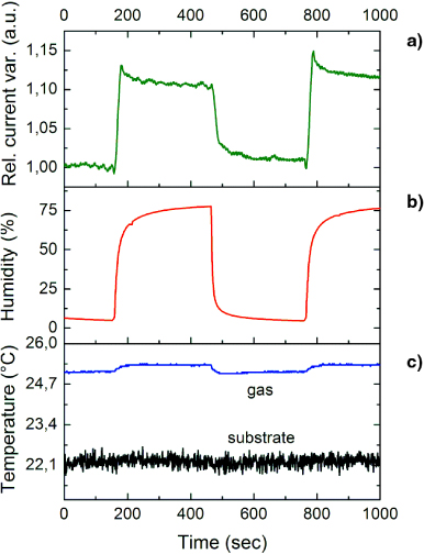
Figure 2. Relative current variation at a fixed bias voltage of 1 V of a 5 nm sensor device (a), during 75% humidity exposure (b), together with gas and substrate temperatures (c).
Download figure:
Standard image High-resolution imageTo evaluate the quantitative sensitivity of the devices, the humidity was increased in a stepwise fashion. Figure 3(a) summarizes the response behavior for sensor devices (referenced to 5% humidity) with different layer thicknesses, ranging from 5 to 60 nm. Clearly recognizable, the strongest response is found for the 10 and 5 nm devices. While devices above 20 nm layer thickness show a broadly linear dependency, the 10 nm and, in particular, the 5 nm device reveal higher sensitivities with a further saturating behavior, indicating that the entire quasi-2D volume is involved for very thin layers. Figure 3(b) summarizes the response factor for all thicknesses at a humidity level of 75% and reveals a strong increase for very thin devices. Figure 3(c) shows the isobaric substrate temperature dependency of the devices under N2 exposure with 2.5% humidity level at ambient pressures. The temperature dependency is clearly found to be stronger for thinner devices. Taking into account the substrate and gas temperatures, shown in figure 2(c), a relevant temperature window from 20 to 26 °C can be defined as the inaccuracy range, which is indicated by the vertical red bar in figure 3(c). The related maximum variation (horizontal green bar in figure 3(c)) is found to be less than 2% for the 5 nm device (compared to the 12% humidity response) and less than 0.5% for the 50 nm device (compared to the 2.5% response). Considering the real gas temperature variation of 0.3 °C during humidity variation (in contrast to the indicated 6 °C interval), it is obvious that the real temperature influence is virtually negligible. Hence, a temperature dependency as the main driving force can be excluded. Considering again the strongly increasing sensitivity for thinner devices (figure 3(b)), the sensing effect is more likely related to a thin surface layer (quasi-2D) than to the bulk volume (3D).
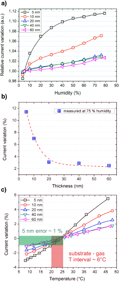
Figure 3. (a) Quantitative current variation as a function of the humidity for different layer thicknesses, normalized to 5% humidity; (b) current response at 75% humidity for different device thicknesses; (c) thermally induced contribution for different thicknesses. The red bar indicates the substrate–gas temperature interval (figure 2(c)) while the green bar reveals a maximum influence of 1% for thinnest devices, thus excluding temperature effects as the main driving force.
Download figure:
Standard image High-resolution imageBefore an interpretation of the response mechanism can be derived, the selectivity must be investigated as well. Figure 4 shows the response of a 20 nm device in the presence of O2 (blue) and CO2 (red) compared to the humidity response (green). In order to reveal whether there is any sensor response to O2 and CO2, both gases were used purely at ambient pressure. Please note that the ground level of the green curve represents the state under pure N2 conditions, which is found to be identical compared to vacuum conditions. From these observations we attribute the observed sensing effect mainly to the dipolar character of the H2O molecule, since O2, CO2, and N2 did not show any influence. In the next paragraph we want to substantiate this by a more quantitative treatment of the problem.
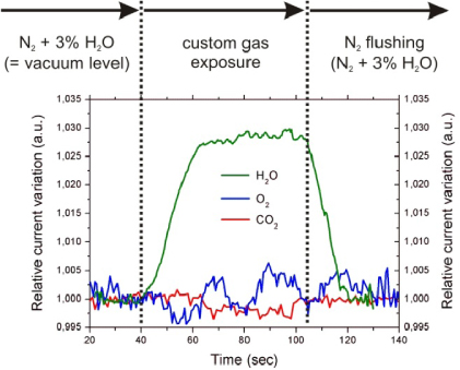
Figure 4. Response behavior of a 20 nm sensor device during exposure to humidity (green), O2 (blue), and CO2 (red). Please note that the initial base level is identical to the vacuum level.
Download figure:
Standard image High-resolution imageIt is known that focused electron beam induced deposition from a MePtCpMe3 precursor results in a nanogranular material consisting of metallic nanoparticles which are embedded in a non-conducting carbonaceous matrix. The transport mechanism is therefore not based on classical percolation of touching metallic particles but related to a tunneling effect in the correlated variable range hopping regime (c-VRH) [14, 25, 29]. In this regime charge transport is realized over a wide temperature range by inelastic co-tunneling. A decisive quantity for the charge transport is the energy associated with the charging that occurs if an excess electron hops onto a metallic grain whose capacitance is very small due to the small particle size of about 2–3 nm. The average or effective charging energy in a (disordered) granular metal depends furthermore on the average background charges stemming from trapped charges in the insulating matrix. This effect leads to an effective reduction of the charging energy. Finally, the electric polarizability or dielectric properties of the insulating matrix govern the screening capability of the granular metal. To explain the working principle that we suggest for the sensor function, a closer look at these dielectric properties of the carbon matrix in between the Pt particles is needed. In the presence of polar molecules reversibly adsorbed on the surface of the granular metal deposit, and also within the skin depth in the volume, the polarizability is enhanced. This leads to a reduction of the effective charging energy and facilitates charge transport via inelastic (co-) tunneling. This principle would explain the reversible character, the insensitivity to non-polar molecules, and, in particular, the strong dependency on the thickness, since only a very thin surface layer can contribute to such an effect. The sensitivity then depends on the ratio of the active skin volume to the unaffected volume. This ratio becomes determining when the layer thickness is in the range of the skin depth. Please note, reference experiments with carbon deposits in the range of 15 nm thickness showed neither a detectable current through the device nor a response to humidity exposure.
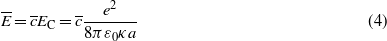
A quantitative estimate of the sensor effect can be obtained from the following derivation. The temperature-dependent conductivity in the c-VRH regime follows the relation (we follow the notation in [24])
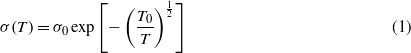
with T0 the activation temperature, given by
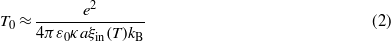
with κ as the effective dielectric constant, a being the grain diameter, ε0 the dielectric constant, kB the Boltzmann constant and the inelastic co-tunneling distance ξin(T) given by
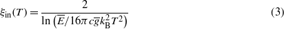
with  as geometrical average value of the electron–hole-excitation energies during charge transport through the nanogranular metal. The geometrical average of the dimensionless tunneling coupling strength between the particles (normalized to the quantum conductance) is denoted as
  . The constant c is equal to 1 as long as the tunneling coupling strength is in the weak coupling regime, i.e.
  , which is the case for our PtC deposits. For
  we set
with EC as the Coulomb charging energy for a spherical particle with diameter a. To account for a reduced Coulomb charging energy due to trapped charges in the insulating carbon matrix and the entailed potential fluctuation, we set  . Finally, we define the sensitivity factor λ as the relative conductivity variation Δσ/σ normalized by the relative dielectric constant variation Δκ/κ:
As can be seen, λ is high for small particle diameters a and low temperatures T. For a = 3 nm,T = 300 K,κ = 2, and  ranging from 10−3 to 10−2, it follows that a 1% dielectric constant variation causes a conductivity variation of more than 7% for a monolayer system. Please note that ξin actually depends on E and
  , which themselves depend on κ. However, the
  dependence is weak due to the logarithm, whose argument is always significantly larger than 1. An example for the overall dependence of the sensitivity factor on
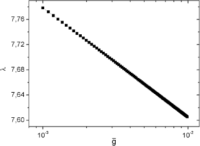
  is shown in figure 5. The dependence of
  on k is only implicit. Together with the experimental results, this theoretical analysis provides a first step in the understanding of the working principle of the nanogranular gas sensing devices introduced here. Further research is needed to verify the assumed polarization effect.
Figure 5. Sensitivity factor λ in dependency on the dimensionless tunneling coupling strength between particles  , revealing only a weak dependency, which is essential for the reliability of the correlated estimation for λ as a function of Δκ.
Download figure:
Standard image High-resolution image
3. Conclusions
We have demonstrated a new gas sensing concept based on a nanosized PtC metal-matrix system using focused electron beam induced deposition as a direct-write fabrication method. The active layer consists of homogeneously dispersed Pt nanocrystals (2–3 nm) embedded in a carbon matrix and responds in the presence of polar water molecules with an increasing current at constant device voltage. Furthermore, the response is of quantitative character and the sensitivity is enhanced with decreasing PtC layer thickness. Another advantage of this concept is the reversible character without any complex reformation procedures by means of temperatures, chemistry or special voltage/current profiles. Temperature effects as the main driving force could be excluded and the sensors did not show a response to non-polar N2, O2, CO2 or during a change from ambient pressure to vacuum conditions. The sole response to water molecules is attributed to its dipole moment and its interaction with the carbon matrix between the Pt nanocrystals. It is suggested that the polar H2O molecules increase the effective dielectric constant of the carbon matrix, which is relevant for the electrical transport (in-plane component). This leads to a reduction of the effective charging energy and facilitates charge transport via inelastic (co-) tunneling, leading to an increasing current. The model can explain the reversibility and the increasing response for very thin devices, since from a physical point of view only the topmost layers should contribute to such a variation. This hypothesis holds also from theoretical considerations and calculations both qualitatively and quantitatively. Expanding these considerations to a condensed gas on the sensor element, an even stronger effect would be expected. This behavior has already been observed in first experiments where condensed phases (humidity > 90%) yield responses of more than 2000% (see figure S3 available at stacks.iop.org/Nano/24/305501/mmedia), facilitating applications in liquid environments since no irreversible effects have been observed (e.g. wetting sensors). The practical advantage of the presented sensor concept is the fast direct-write fabrication in a single step (a 5 nm device can be prepared in 30 s), the possibility to deposit such devices even on non-flat surfaces where classical resist based techniques are complicated, the selective and quantitative character, as well as the reversibility without any special reformation procedures requiring temperature or special environments. In combination with multi-electron-beam sources, currently introduced in industry, this sensor concept can open interesting possibilities for special purposes.
4. Methodology
PtC deposition were performed with a FEI NOVA 200 dual beam system equipped with a Pt gas injection system (GIS) (FEI) using MeCpPt(IV)Me3 as precursor. The working distance during deposition was 4.9 mm, with a chamber base pressure of 2 × 10⁻⁵ mbar. The Pt precursor was heated to 45 °C at least 1 h prior to deposition and the GIS was placed 150 μm above the substrate. To provide a stable thermodynamic precursor/substrate situation, the GIS was opened at least 5 min prior to deposition, leading to a saturation pressure of about 3 × 10⁻⁵ mbar. The deposition was performed at 5 keV/1.6 nA, with in-focus conditions via the internal patterning generator. The pattern footprint was set to 20 μm × 5 μm and a serpentine scanning strategy was used with a point pitch of 13.5 nm and 10 μs pixel dwell time. To achieve different thicknesses, the loop number was varied and correlated with atomic force microscopy (AFM) and electrical measurements to derive calibration curves for further device fabrication. After deposition the GIS was withdrawn and a clearance period of at least 5 min was introduced before the first electrical control measurements were performed. The PtC sensors were deposited across two or four 40 nm thick gold electrodes (2 μm line/space width, 40 nm thick), which were pre-patterned on 500 nm SiO2 (Si substrate) via e-beam lithography (Raith E-Line). The lines were conducted via macroscopic pads to an in-house designed active in situ sample holder for the scanning electron microscope chamber. A Keithley 230 (Keithley, USA) was used as constant voltage source in combination with a Keithley 616 (Keithley, USA) as an ampere meter with a proportional voltage output, connected to a National Instruments—DAQCard-6036E card (National Instruments, USA) for electrical in situ pre-characterization. Data acquisition was performed via LabVIEW software (V10.0, National Instruments, USA). The devices were then exposed to ambient conditions and placed into another ex situ sample holder to perform long-time and I/U measurements. Gas exposure measurements were done in a custom-made gas measurement system, including a probe chamber with ∼0.14 dm3 total volume equipped with a Peltier element, a Pt-100 sensor (on Peltier Element) and a SHT 15 temperature/humidity sensor (Sensirion, evaluation kit EK-H2). Gas flow and relative humidity concentration were regulated via mass flow controllers (Teledyne Hastings HFC-302 with Schaefer Flow-Controller Power Supply PSCT 4; max. 1 and 5 SLPM (1.69 Pa m3 s−1 and 8.4 Pa m3 s−1) nitrogen, respectively). Humidified N2 was generated by bubbling through de-ionized water at room temperature with a flow of N2 through a wash flask. The desired humidity values were obtained by the ratio of humidified and dry N2, automatically adjusted by the two mass flow controllers specified above. O2 and CO2 exposure were performed without mixing with other gases (100% exposure) using gases with purity grades of 5.0 and 4.5, respectively. Humidity and temperature data were recorded via a custom LabView program and electrical characterization of the sensors during gas exposure was done using an Agilent B1500A Parameter Analyzer. Voltage-dependent preliminary experiments on deposit-free reference electrode structures were measured at very high humidity levels (>90%), revealing a H2O related influence for operating voltages above 1.5 V (see figure S4 available at stacks.iop.org/Nano/24/305501/mmedia). Therefore, all active measurements were performed at a maximum voltage of 1 V. Reference measurements included patterning without precursor gas for more than 40 min, resulting in a carbon deposit of about 15 nm thickness. Electrical measurements showed neither a detectable current through the deposits nor a response to humidity exposure including the condensed phases. AFM measurements were performed with a Dimension 3100 microscope (Digital Instruments, Bruker) operated with a Nanoscope IVa controller and a Hybrid XYZ Closed Loop scan-head. The entire system is placed in a glove box (MBraunUnilab) operated in a dry N2 atmosphere (H2O and O2 < 0.1 ppm). Energy dispersive x-ray spectroscopy (EDS) was performed in a NOVA 200 system using an Xflash silicon drift detector (4010, Bruker AXS) with short acquisition times of 60 s.
Acknowledgments
FK and HP gratefully acknowledge support from Professor Dr Ferdinand Hofer, Professor Dr Gerald Kothleitner, DI Roland Schmied, Martina Dienstleder and Manuel Jelinek. KS and AK acknowledge the financial support of the Styrian Government (projects BioOFET 2, GZ:A3-11.B-36/2010-5).