
Abstract
We present a methodology for preparing silicon nitride nanopores that provides in situ control of size with sub-nanometer precision while simultaneously reducing electrical noise by up to three orders of magnitude through the cyclic application of high electric fields in an aqueous environment. Over 90% of nanopores treated with this technique display desirable noise characteristics and readily exhibit translocation of double-stranded DNA molecules. Furthermore, previously used nanopores with degraded electrical properties can be rejuvenated and used for further single-molecule experiments.
Export citation and abstract BibTeX RIS
1. Introduction
Over the past two decades, nanopores have emerged as a versatile tool for the detection and characterization of single molecules. In a typical nanopore experiment, charged biomolecules are driven through the pore by an electric field and the resultant change in ionic current through the pore can be used to infer a molecule's size, composition and conformation [1]. Fueled by the goal of single base resolution for rapid, high-throughput DNA sequencing, both solid-state and organic nanopore sensing platforms are currently the targets of intense investigations [2]. While biological pores offer greater sensitivity and often lower noise properties, they are limited to very specific operational conditions due to the fragility of the supporting lipid bilayer, and by their fixed size to study very small molecules, such as single-stranded DNA. Solid-state nanopores, on the other hand, are a promising alternative as they offer increased durability, size and shape tuning ability, and are naturally suited for integration with wafer scale technologies [3, 4]. Typically drilled in thin (10–50 nm) insulating membranes using a tightly focused beam of electrons in a transmission electron microscope (TEM) [5], the resultant pore diameter and shape can be controlled by adjusting the beam parameters used in the fabrication process [6, 7] or by subsequent treatment with a scanning electron microscope (SEM) [8]. Such control over size and geometry is crucial for many nanopore applications, such as the study of DNA–protein interactions [9], force spectroscopy [10] and ultimately DNA sequencing [2].
Despite their advantages, the use of solid-state nanopores continues to face fundamental challenges that limit their effectiveness for single-molecule studies. For instance, size manipulation requires the use of elaborate equipment such as a TEM, which must often be performed off-site under non-biosensing conditions, increasing the overall time and expense associated with fabrication. Such techniques for fine-tuning nanopore size, however, are not optimal, as the actual size of the nanopore following the harsh chemical treatment, plasma cleaning or immersion in aqueous solutions required for molecular recognition experiments is often different from that determined from electron microscopy (EM) [11]. From a practical point of view, solid-state nanopore devices are often very noisy, resulting in a wide range of studies that focus on the treatment of noise in ionic current measurements. For instance, some groups focus on reducing dielectric noise arising from the properties of the nanopore chip through the addition of insulating layers such as polydimethylsiloxane (PDMS) [12] or polyimide layers defined by photolithography [13]. Also problematic is the variability in surface charge distribution [14] and non-uniform pore profile [15], which can influence the noise characteristics and I–V properties from pore to pore, often resulting in a tendency for pores to clog during the course of an experiment, after which they are no longer functional. Altogether, these effects can drastically reduce the yield of nanopores that can be used in experiment. Thus, reproducible fabrication of reliable nanopores remains a challenge not only for the academic research environments, but most importantly, for the commercialization of any nanopore-based technology.
In this article, we present a method of improving the noise performances of pre-drilled nanopores, while accurately fine tuning their size with sub-nanometer resolution in situ, i.e. directly in a buffered electrolyte solution. Our system, as shown in figure 1(a), consists of a custom-built Teflon cell with two 500 μl reservoirs (1 M KCl, pH 8.0) separated by a 30 nm thick silicon nitride (SiNx) membrane, containing a nanopore drilled by TEM. While typical experiments are run at relatively low voltages (0.1–0.5 V), we find that by applying a larger potential difference (6–10 V) across a nanopore using Ag/AgCl electrodes, we are able to precisely modify the size and noise characteristics of the nanopore. Nanopore size is controlled via the removal of pore surface atoms in a strong electric field (0.20–0.33 V nm−1). By applying short, high electric field pulses, we are able to precisely increase the effective diameter of a nanopore in small steps depending on the strength and duration of each pulse and the original size of the nanopore. In addition to providing sub-nanometer size control, treatment with high electric field pulses yields reproducible low-noise behavior and optimized I–V characteristics. As a result, nanopores that would have otherwise been discarded due to high 1/f noise are made functional for molecular translocation studies. Moreover, the approach enables the recycling of previously used and seemingly clogged nanopores, as the process removes parasitic debris and/or physisorbed molecules and allows, in most cases, the previously used nanopores to regain low-noise characteristics. A significant advantage to using this technique for controlling and assessing nanopore diameter is that it is performed in situ in an aqueous environment under typical experimental conditions using standard laboratory equipment. While TEM is used to initiate nanopore formation, the final pore size and geometry is controlled under the same experimental conditions used for interrogating biomolecules without requiring further use of specialized electron microscopes or harsh chemical treatment. Thus the cost, time and complexity associated with fine tuning the nanopore size using standard EM approaches are significantly reduced, and fabrication yield is increased to over 90%.
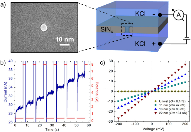
Figure 1. (a) A cross-sectional schematic of our nanopore device. A 30 nm thick silicon nitride window contains a representative TEM-drilled nanopore (zoom). An external power supply and current amplifier are used to control high voltage pulses for nanopore enlarging and cleaning (see methods section 4.2). (b) Increasing ionic current (blue) upon treatment with high voltage pulses. Voltage (red) is alternated between 2 s pulses of 8 V and measurement periods 7 s at 400 mV. Current is sampled at 1 kHz and averaged every hundred points for display. (c) I–V characteristics of various enlarged pores 30 min after enlarging. The yellow circles are data from an untreated pore that did not wet, and thus had almost no conductance. Upon the application of high field pulses, the pore wetted and was enlarged to 22 nm (red inverted triangles). Green squares and blue triangles were pores enlarged to 11 nm and 16 nm, respectively. In the voltage range of ±200 mV, the pores have a constant conductance which was used to calculate pore diameter.
Download figure:
Standard image2. Results and discussion
2.1. Control of nanopore size
The process for preparing a nanopore for a molecular recognition experiment involves the automated cyclic application of high electric field pulses produced by stepping the potential up to 6–10 V. As the conductance G of nanopores subjected to a potential bias greater than 4 V is no longer Ohmic and would yield unrealistic nanopore diameters (supplementary information figure S1 available at stacks.iop.org/Nano/23/405301/mmedia), a low voltage bias (400 mV) is applied after each high field pulse. This allows us to accurately measure the increase in nanopore conductance during growth. As nanopore conductance has been shown to directly depend on the nanopore size, a measure of the conductance can be used to infer nanopore diameter [16–19]. Here, we assume cylindrical pore geometry with an effective length of leff = 15 nm (half of the membrane thickness) using the relationship discussed by Kowalczyk et al (equation (1)) [16] describing the conductance of a nanopore of diameter d in a KCl solution of conductivity σ = 11.3 S m−1. We note that this choice of leff is in good agreement with experimental data of DNA translocation, as discussed in section 2.3 of the text.

Figure 1(b) shows that by applying 8 V pulses of 2 s duration, the ionic current through the nanopore increases in steps of approximately 1.3 nA after each pulse, corresponding to a increase in conductance of ΔG = 3.3 nS. The resultant increase in nanopore diameter per cycle under these conditions is ∼0.4 nm. While variability in membrane thickness, surface chemistry and initial nanopore geometry yields different growth rates from pore to pore, the magnitude and duration of each high field pulse can be adjusted to precisely control the amount of growth per cycle. Due to the relatively high capacitance of the nanopore device, measurement periods at 400 mV were extended to 7 s to allow for the capacitive current to dissipate and the faradaic current to stabilize after each voltage pulse. While an external power supply and current amplifier are used to provide the necessary high voltage and measure the resultant ionic current during enlarging, we can easily revert back to a low-noise experimental setup (see methods section 4.2). In the sub-1 V voltage range, enlarged pores act as ideal Ohmic resistors with linear I–V curves, as shown in figure 1(c). This trend is consistent over multiple enlarged nanopores (N = 20) and we find that the conductance of nanopores treated with high field pulses is stable up to several days after treatment (supplementary information figure S2 available at stacks.iop.org/Nano/23/405301/mmedia). We note that conductance values are constant even after unmounting a nanopore and flushing the system with fresh electrolyte solution, indicating that the observed increase in conductance is not a transient effect caused by local heating of the electrolyte in the nanopore.
In order to further understand the enlargement process, the dependence of nanopore growth on the electric field strength was investigated. From figure 2(a), varying the pulse strength from 6 to 10 V (0.20–0.33 V nm−1) produces quite different growth profiles. In each case, nanopores were immersed in 1 M KCl solution and the pulse duration was kept constant at 2 s. When subjected to a 6 V potential bias, nanopore growth is relatively slow with conductance increasing by ∼25 nS over 1000 s of exposure time (0.03 nS s−1). In comparison, pores subjected to 8 V and 10 V increase in conductance at an average rate of ∼0.10 nS s−1 and 0.63 nS s−1, respectively. We note, however, that several different growth regimes are observed depending on the stage of enlargement and the applied bias. While nanopore growth at 6 V is approximately linear throughout most of the time window shown, the growth rate increases over time at 8 V and more drastically at 10 V. Additionally, nanopore growth appears to initially slow for the first 200 s of exposure to 6 V and 8 V, as highlighted in figure 2(b). For the 10 V case, this initial growth is characterized by a sharp increase in conductance from 10 to 14 nS after ∼85 s. From noise characteristics of the nanopore before and after enlarging, this jump in conductance is attributed to complete wetting of the nanopore, as discussed later in this paper.
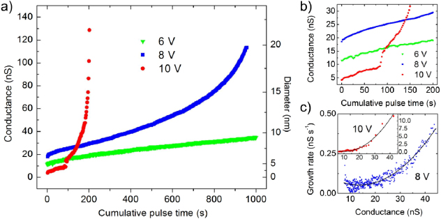
Figure 2. (a) Enlargement of nanopores upon 2 s pulses of 6 V (green triangles), 8 V (blue squares) and 10 V (red circles) in 1 M KCl. After each pulse, current measurements were acquired at 400 mV at 1 kHz for 7 s. After 2 s of measurement, current values over the next 5 s were averaged and used to calculate the conductance of the nanopore, shown as a function of the cumulative pulse time of the experiment. (b) An enlarged view of the first 200 s of nanopore growth showing a decrease in growth rate with time. At 10 V, complete wetting of the nanopore is seen as a sharp increase in conductance after 85 s. (c) Growth rate of as a function of nanopore conductance following each 8 V (blue squares) and 10 V (red circles) pulse appears approximately parabolic (fits to second degree polynomials shown as solid black lines). In (c), while the entire growth profile using 8 V pulses is shown, only growth rate values after 85 s of enlargement using 10 V pulses are displayed.
Download figure:
Standard imageWhen subjected to pulses larger than 6 V, nanopore growth rate increases throughout the enlarging process; that is, larger pores grow faster than smaller ones. This is illustrated in figure 2(c), where the growth rate of the nanopores subjected to 8 and 10 V increases as a function of the conductance measured before each high electric field pulse. For the 10 V case, growth rate is plotted from data acquired after the initial 100 s of enlarging, following complete wetting of the nanopore. We find that in the conductance window shown, nanopore growth rate is approximately parabolic, ranging between 0.01–0.40 nS s−1 and 0.01–11 nS s−1 for 8 V and 10 V applied biases, respectively. Interestingly, this increase in conductance corresponds to a growth rate of less than 0.1 nm per second, assuming a cylindrical nanopore with an effective length of 15 nm. This method is thus very powerful for obtaining precise control over final nanopore size. It should also be noted that for nanopores of conductance greater than 150 nS, growth is less predictable for biases of 8–10 V, although pulse strength can be tuned to offer better control.
While it is clear from the different growth rates of the nanopores shown in figure 2 that the strength of the electric field plays a significant role in the enlarging of nanopores, a complete understanding of the growth process is not yet clear. In fact, several mechanisms are likely involved in the growth process. The initial slowdown in the increase of the growth rate (figure 2(b)), which seems common to many nanopores we investigated, could be related to the initial modification of the nanopore profile or to the removal of weakly bound residual carbonaceous contamination that may be left over from the TEM drilling and imaging process [20]. But as the nanopore is enlarged, the increasing growth rate for large conductance values in figure 2(c) seems to indicate a relationship between growth rate and the amount of current passing through the nanopore, as the applied bias and pulse duration are kept constant throughout the experiment. However, pore to pore variability in growth rate under identical experimental conditions (supplemental information figure S3 available at stacks.iop.org/Nano/23/405301/mmedia) as well as with varying ionic strength of electrolyte solution (supplemental information figure S4 available at stacks.iop.org/Nano/23/405301/mmedia) makes an elucidation of a complete mechanism difficult. Ascertaining the exact roles of power dissipation, electro-osmotic flow, resistive heating and electrochemistry occurring at the nanopore surface is beyond the scope of this article and is the subject of ongoing investigation. From a practical point of view, however, cyclic application of high field pulses provides a means of controlling nanopore size with exceptional precision, as the nanopore diameter can be increased in sub-nanometer steps in an automated fashion simply by varying the pulse strength and level of ionic current in situ under experimental conditions.
2.2. Noise reduction
In addition to providing control over pore size, application of short high electric field pulses significantly reduces low frequency noise in nanopore current measurements. This so-called 1/f noise is thought to arise from fluctuations in the number of charge carriers occupying the nanopore in accordance with Hooge's phenomenological relation [12, 21, 25]. In solid-state nanopores studies, excessive 1/f noise is typically observed when nanopores fail to completely wet [22], or when, over the course of an experiment, translocating molecules adsorb to the nanopore wall [23, 24], often resulting in a partial clog. As these sources of noise can significantly complicate signal analysis, nanopores initially exhibiting high 1/f noise are typically discarded when standard procedures such as piranha cleaning and oxygen plasma treatment fail to mitigate these effects and produce clean signals [25]. While functionalization of the nanopore walls [26–28] is a potential option for preventing non-specific adsorption, the addition of organic molecules may not be desirable for some applications and involves additional preparation steps. Thus, due to the difficulty and expense associated with nanopore fabrication and preparation, a simple method for systematically and reproducibly reducing 1/f noise and rejuvenating clogged nanopores is of great practical importance for improving the yield of those usable for experiment.
By applying short high field pulses, we find that such pores are readily and rapidly cleaned in situ, without risking accidental damage to the membrane or requiring lengthy procedures associated with manipulating the nanopore chip. By maintaining a short pulse time ( < 500 ms), we are able to reduce low frequency noise while avoiding enlarging the nanopore. Figure 3(a) shows the power spectral density (PSD) plots of two nanopores for an applied bias of 200 mV both before and after the application 8–10 V pulses of 200 ms duration. As the dielectric properties of the SiNx membranes and the amplifier headstage are the predominant sources of noise above 10 kHz, these portions of the PSD remain relatively unchanged from pore to pore. Below ∼1 kHz, however, low frequency noise varies as 1/fα with 0.94 < α < 1.5 and can be significantly lowered upon treatment with high electric fields. For instance, the orange curve in figure 3(a) is a typical PSD of a pore that had become irreversibly clogged during a DNA translocation experiment and two separate washes in piranha solution at 75 °C for 30 min were unable to regenerate a low-noise current trace. The red curve, however, shows the PSD of an 11 nm (G = 47.0 nS) clogged pore that has been cleaned using 200 ms pulses of 10 V. In this example, 2 pulses were enough to remove the source of noise and leave a clean nanopore surface with a very stable conductance, illustrated by a three orders of magnitude decrease in low frequency noise in the below 500 Hz.
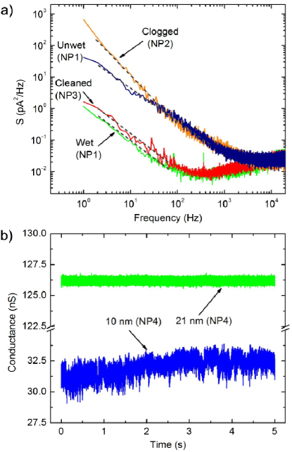
Figure 3. (a) PSD versus frequency at 200 mV low-pass filtered at 100 kHz, using a 4-pole Bessel filter, for three pores before and after treatment with high electric field pulses. Blue and green curves correspond to the same 7 nm pore (NP1) before and after complete wetting using 8 V pulses of 200 ms, respectively. The orange curve shows a typical PSD of a clogged, high-noise nanopore (NP2) that would typically be deemed unusable for experiment. The red curve shows the PSD of a previously clogged pore (NP3) that was cleaned using two 10 V pulses of 200 ms and regained low-noise characteristics. Dashed gray lines illustrate the 1/fα dependence of noise at low frequencies, where 0.94 < α < 1.5. (b) Current traces at 200 mV for an incompletely wetted 10 nm pore (blue, NP4) that was enlarged to 21 nm (green) using 8 V pulses of 2 s duration. Data was acquired at 250 kHz, low-pass filtered at 100 kHz using a 4-pole Bessel filter and averaged every 5 data points for ease of viewing.
Download figure:
Standard imageTo illustrate the effectiveness of this method for reducing 1/f noise in incompletely wetted nanopores, an unused ∼7 nm pore (as determined after TEM drilling) that failed to completely wet despite cleaning with piranha solution (blue curve in figure 3(a)) was treated using 8 V pulses of 200 ms duration. While a total of 7 pulses were applied, nanopore conductance did not significantly change after the first one, indicating that a single pulse was sufficient to completely wet the pore. The PSD of the nanopore upon treatment (green curve) exhibits nearly two orders of magnitude reduction in low frequency noise, which varies as 1/fα with α = 0.94, consistent with previously characterized low-noise SiNx nanopores [12]. Moreover, the nanopore exhibited a conductance of 19.6 nS, appropriate for a 15 nm long cylindrical nanopore of 7 nm diameter. Interestingly, we find that once a nanopore has completely wetted, low-noise characteristics are maintained through subsequent enlarging. figure 3(b) shows current traces of a 10 nm pore (as determined after TEM drilling) before and after complete wetting and enlargement to 27 nm (G = 126 nS) using 8 V pulses of 2 s duration as described above. Clearly, analysis of DNA translocation before treatment with high electric fields would be extremely challenging if not impossible, while the enlarged, treated pore exhibits substantial improvement in stability.
The complete wetting of a nanopore using a strong electric field has been previously observed and is understood as a lowering of the potential energy barrier for complete wetting of the pore via the alignment of the dipole moment of water vapor molecules [29, 30]. However, the nanopores investigated in those studies were hydrophobically modified for the application of nanopore gating and were either fabricated with conical geometry in polymer films or were too large to be suitable for single molecule detection. Moreover, the electric field strengths reached in these studies were over an order of magnitude less than those discussed here, a thorough investigation of the noise characteristics of treated nanopores was not performed and there was no indication of nanopore enlargement. While high electric fields have also been previously used to facilitate wetting of SiNx nanopores capable of detecting and characterizing DNA molecules [31], to the best of our knowledge our study is the first to present data characterizing the process and experimental evidence revealing that low frequency noise can be effectively reduced. Furthermore, we find that treating nanopores with high electric field pulses produces low-noise current signals with a yield of over 90% (supplementary information figure S4 available at stacks.iop.org/Nano/23/405301/mmedia). Currently, it is common to reject a large portion of nanopores due to high noise, current rectification and incomplete wetting. This method shows great promise as a means for reproducibly preparing functional nanopores for molecular recognition experiments.
2.3. Detection of DNA translocation
We further characterized these high electric field treated pores by performing DNA translocation experiments to evaluate their performances as single-molecule sensors. Pores enlarged to diameters ranging from 10 to 35 nm (40–490 nS in 2 M KCl) were used to detect λ DNA (48.5 kbp, New England BioLabs). Upon enlarging each pore, both electrolyte reservoirs were flushed with 2 M KCl (σ = 21.5 S m−1) buffered at pH 8.0 (higher salt concentration was used to increase signal to noise of translocating molecules) and double-stranded (ds) λ DNA was introduced into the cis chamber at a working concentration of 1 μg ml−1. Figure 4(a) shows that at a bias of 150 mV, conductance spikes become clearly visible upon the addition of DNA as molecules are electrophoretically driven through the 11 nm and 32 nm pores (87 nS and 432 nS in 2 M KCl, respectively). As expected for nanopores of these diameters, multiple quantized blockage depths are observed corresponding to the translocation of folded and unfolded DNA molecules [32]. In figure 4(b), the equidistant separation of peaks in histograms of the nanopore conductance during translocation events confirms the presence of multiple discrete blockage states during translocation. We note that the reduction of 1/f noise in the open pore current signal, a result of the enlarging process, produces histograms with easily resolvable peaks. Furthermore, while nanopores would eventually clog throughout the course of a translocation experiment, low-noise open pore conductance values were often regained with short (100–200 ms) pulses of 6–10 V. Nanopore rejuvenation for further experimentation through treatment with high electric fields is thus of great benefit for improving the efficiency and lifespan of nanopores.
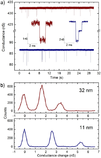
Figure 4. (a) Detection of dsDNA using pores enlarged to 11 nm (87 nS, blue) and 32 nm (432 nS, red). Upon introduction of λ DNA and applying a 150 mV bias, current blockades appear in discrete quantized amplitudes corresponding to the translocation of zero, one and two dsDNA strands through the pore (inset). Current data was filtered using a 10 kHz low-pass Bessel filter for display. (b) Histograms of the event conductance levels for DNA translocation events through the nanopores shown in (a). Peaks corresponding to the quantization of conductance during translocation are clearly resolved.
Download figure:
Standard imageInterestingly, the change in conductance of ΔG = 1.7 nS produced by dsDNA translocating through the 32 nm pore is smaller than that of ΔG = 2.6 nS for the 11 nm pore. This is consistent with models described elsewhere [16] describing the increased role of access resistance in determining the change in nanopore conductance upon the translocation of dsDNA through large pores. This result confirms that the original nanopore has in fact been enlarged and that the rest of the membrane retained its integrity and did not conduct current, as otherwise DNA translocations would have exhibited a similar drop in conductance as the 11 nm pore. By fitting the ΔG values for enlarged pores with the model proposed by Kowalczyk et al [16] given by equation (2), we find that the effective pore length of treated nanopores can range from 11 to 16 nm, showing that the assumed pore length of 15 nm provides a good fit for dsDNA translocation through enlarged nanopores.

Here, G is given by equation (1) and dwith DNA, given by (3) is the effective diameter of the pore containing dsDNA of diameter dDNA = 2.2 nm.

3. Conclusion
We have presented a novel method for both fine-tuning nanopore size with sub-nanometer precision and reducing low frequency noise in current measurements using short high electric field pulses. Treatment of pores in this fashion significantly improves the yield of nanopores that can be successfully used in DNA translocation experiments and demonstrates that size control is possible in situ under experimental conditions without requiring the use of an elaborate apparatus. The fact that size control is so accessible facilitates a wide range of potential micro- and nanopore studies, from the investigation of DNA–protein interactions to the translocation of viruses and small cells.
4. Materials and methods
4.1. Nanopore fabrication
Nanopores used were fabricated in 50 μm × 50 μm, 30 nm thick free standing silicon nitride membranes supported on a 200 μm thick silicon frame purchased from Norcada (NT005X). In each membrane, we drilled a sub-10 nm pore using a tightly focused beam of electrons in a JEOL-2100 TEM operated at 200 kV accelerating voltage. Nanopores were drilled at 600k magnification using the condenser aperture of spot size=2 and α = 3.
4.2. Protocols and instrumentation
Prior to mounting the nanopore chips in solution, nanopore chips were prepared for experiment by cleaning them for 30 min in piranha solution (3:1 H2SO4:H2O2) at 75 °C. The chips are then thoroughly rinsed in filtered, degassed deionized water and immediately mounted in the liquid cell containing filtered, degassed 1 M KCl 10 mM HEPES buffered at pH 8.0 at room temperature or the salt concentration indicated in the text. We used a polytetrafluoroethylene cell to mount the nanopore chip between two liquid reservoirs, as described in [12]. Custom-made silicone gaskets sandwich the chip to ensure a gigaohm seal. The cell is placed in a Faraday enclosure to reduce electrical noise. Ag/AgCl electrodes immersed on both sides of the pore were used to measure ionic current when connected to a current amplifier. A patch-clamp amplifier (Axopatch 200B, Molecular Devices) was used to record ionic current for power spectrum density calculations, I–V characterization and DNA translocations. Data acquisition was performed using custom-designed LabVIEW software controlling a National Instruments PCIe-6351 DAQ card. Data were low-pass filtered at 100 kHz using the Axopatch 200B 4-pole Bessel filter and sampled at 250 kHz. For applying voltage pulses up to 10 V between each electrode, the PCIe-6351 DAQ card was used, while a Keithley 428 current amplifier was used to measure the resultant current at a sampling frequency of 1 kHz. Alternating voltage pulses and conductance measurements were controlled using custom-written LabVIEW software.
Acknowledgments
This work was supported by the Natural Sciences and Engineering Research Council of Canada, the Canada Foundation for Innovation and the Ontario Research Fund. The authors would like to thank Y Liu of the Centre for Catalysis Research and Innovation for aid in nanopore fabrication and characterization and L Andrzejewski of the University of Ottawa Physics department for valuable discussions and technical support.