
Abstract
Imprinted silver nanovoid arrays are investigated via angle-resolved reflectometry to demonstrate their suitability for plasmonic light trapping. Both wavelength- and subwavelength-scale nanovoids are imprinted into standard solar cell architectures to achieve nanostructured metallic electrodes which provide enhanced absorption for improving solar cell performance. The technique is versatile, low-cost and scalable and can be applied to a wide range of organic semiconductors. Absorption features which are independent of incident polarization and weakly dependent on incident angle reveal localized plasmonic modes at the structured interface. Metallic nanostructure–PCPDTBT:PCBM samples demonstrate absorption enhancements of up to 40%. The structured interface provides light trapping, which boosts absorption at wavelengths where the semiconductors absorb poorly.
Export citation and abstract BibTeX RIS
1. Introduction
The field of plasmonics has advanced tremendously in recent years [1, 2], largely enabled by significant advances in nanofabrication technology. Total light absorption has been theoretically as well as experimentally investigated for periodic nanostructured metal surfaces [3, 4]. Teperik et al [5] shows omnidirectional absorption of light for close-packed metallic nanovoids. Solar cells stand to benefit greatly from plasmonic light trapping, where plasmonic excitation leads to an increased absorption of light in the adjacent semiconductor film and a consequent enhancement in charge-carrier generation (or, in the case of organic semiconductors, exciton generation) [6–10]. Previous reports have demonstrated that metallic nanovoid arrays are capable of hosting localized as well as propagating plasmonic excitations and are therefore extremely interesting for incorporation into solar cells in the form of nanostructured electrodes [11–13]. Here we investigate metallic nanovoid arrays fabricated using a simple, scalable, low-cost nanoimprint technique and assess their potential for trapping incident light in adjacent films. We first address plasmonic excitation on imprinted transparent dielectric–silver nanovoid interfaces. These excitations can decay radiatively via out-coupling to photons or non-radiatively via absorption in the silver film. In order to address the suitability of this method for manufacturing highly absorbing solar cells, we then fabricate samples with organic semiconductor (OSC)–silver nanovoid interfaces. We thereby gain an insight into the effect of absorption in the OSC on plasmonic modes at the interface. In samples with absorbing dielectric–silver interfaces, plasmonic excitations have two non-radiative decay channels: absorption in the silver and in the OSC film. Decay via absorption in the OSC film is desirable for solar cells, as this absorbed energy can be converted into electrical current. In contrast, absorption in the silver is a loss mechanism. An efficient transfer of trapped mode energy to absorption in the adjacent OSC film is a requirement for obtaining a significant absorption and hence efficiency enhancement in organic solar cells with structured metallic electrodes. Previous reports of organic–silver systems indicate that energy stored in pure SPP modes [6], localized nanovoid modes [14], and near-field/far-field modes at metallic nanoparticles [15] is indeed efficiently transferred to an adjacent organic film (with an efficiency as high as 95% [6]).
2. Materials and methods
To elucidate the nature of the plasmonic excitation on imprinted nanovoids we first imprint silver nanovoid arrays adjacent to an optically transparent dielectric, PMMA (polymethylmethacrylate). The real part of the refractive index varies between 1.2 and 1.5 in the investigated photon energy range and the imaginary part is negligible [16]. PMMA films of thickness around 300 nm are obtained by spin-coating from a toluene solution (96.9 mg ml−1) for 1 min at 3000 rpm onto 2 cm2 substrates. Quartz substrates are used for spectroscopy measurements and quartz substrates coated with indium tin oxide are used for SEM imaging to minimize charging during imaging. Nanoimprint lithography [14, 17–19] (450 bar, 100 °C, 5 min) is then used to structure the surface of the polymer film. The periodicity of the structured film is equal to that of the stamps, and the feature diameter and height are determined by the imprinting temperature, pressure and duration. Chips of anodized aluminum oxide (AAO) [20, 21] that feature large-area hexagonal lattices of pores are used as stamps. The nanostructured polymer films obtained (figures 1(a)–(d), where (a) and (c) show PMMA films and (b) and (d) show OSC films) are then covered with a layer of silver (nominally 150 nm thick) via evaporation. This silver layer conforms to the topography of the underlying polymer film to produce samples with a metallic nanovoid array interface (figure 1(e)) [14]. Flat reference samples are fabricated in parallel under identical conditions without the imprinting step.
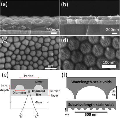
Figure 1. (a)–(d) SEM images of imprinted nanostructures. A layer of indium tin oxide is visible between the structured polymer and the glass substrate in cross-section images ((a), (b)). (a) Transparent dielectric and (b) organic semiconductor wavelength-scale structures (490 nm period) and (c) top view of (a). (d) Top view of organic semiconductor subwavelength-scale structure (95 nm period). (e) Sample and measurement geometry. (f) Scale diagram of wavelength-scale and subwavelength-scale voids (transparent dielectric). Additional SEM pictures are shown in the supplementary information (available at stacks.iop.org/Nano/23/385202/mmedia).
Download figure:
Standard imageTo investigate imprinted nanovoid light trapping in solar cell geometries, we fabricate additional samples with organic semiconductor (OSC)–silver nanovoid interfaces. Here we use an OSC film of poly[2,6-(4,4-bis-(2-ethylhexyl)-4H-cyclopenta[2,1-b;3,4-b']dithiophene)-alt-4,7-(2,1,3-benzothiadiazole)]:phenyl-C61-butyric acid methyl ester (PCPDTBT:PCBM), two components commonly used in organic photovoltaics [22]. Precursor concentrations of 22.2 (PCPDTBT) and 24 mg ml−1 (PCBM) in chlorobenzene (mixed 1:2), and spin-coating conditions (1500 rpm for 1 min) are chosen to obtain films of 100 nm thickness, consistent with optimized solar cells of this type [22].
Stamps with two pore periodicities (490 and 95 nm) are used to fabricate nanovoid arrays of different pitches, which we refer to as wavelength-scale and subwavelength-scale voids respectively. The voids for the dielectric sample (figures 1(a) and (c)) can be well approximated by an array of hemispheres with characteristic void diameters of 470 and 60 nm respectively. The pore depths are 195 and 25 nm respectively (figure 1(f)).
Nanoimprint lithography is performed under identical conditions with the same stamps for the semiconducting composite to fabricate samples that are directly comparable with the transparent dielectric samples. Due to the reduced thickness of the OSC layer (necessary for efficient charge-carrier extraction in solar cells), the voids imprinted with the wavelength-scale stamp have a truncated hemispherical shape (figure 1(b)) and hence a smaller depth (115 nm) than the voids in the dielectric sample (195 nm). Otherwise, the dielectric and OSC samples have equal void period, diameter and depth (see also figure SI.1 available at stacks.iop.org/Nano/23/385202/mmedia).
Specular reflectance spectra (figure 1(e)) are measured from 1.4 to 2.9 eV with a supercontinuum white-light laser source (Fianium SC-450-6) for incidence angles 0°–45°. The incident beam is passed through a polarizer to obtain either TM- or TE-polarized light. The reflected beam is fiber-collected, separated into visible and IR wavelengths via beam-splitters and detected using Ocean Optics QE65000 and NIRQuest spectrometers respectively [11]. Reflectance R is normalized to a flat silver mirror and absorption A is obtained via A = 1 − R. Non-specular reflection is measured to be negligible—indicating that light which would otherwise be out-coupled from the sample as non-specular reflection is preferentially trapped within the sample via coupling to surface modes [11] and or multiple internal reflections. Similar reflectance spectra are measured over the entire area of each sample.
3. Results and discussion
Absorption in the structured dielectric–Ag samples (figures 2(a)–(d)) occurs exclusively in the silver layer as the adjacent dielectric layer absorbs negligibly in this photon energy region. For the wavelength-scale voids, a number of broad absorption features can be seen between 1.9 and 2.9 eV (indicated by the black dashed line in figures 2(a) and (b)), consistent with plasmonic excitation at the nanostructured dielectric–Ag interface. The excitation of these absorption features is strongest for incident angles between 10° and 45°; however, other than this, no strong angle dependence is observed. The similarity between the absorption spectra for TE and TM polarizations indicates that these modes are localized surface plasmons (LSPs), which unlike surface plasmon polaritons (SPPs) are polarization independent for hemispherical nanovoids [2, 11]. This is in qualitative agreement with measured and simulated spectra obtained for similar nanovoid arrays reported elsewhere [11, 13, 23]. Dispersive energy minibands (most prominent in figure 2(b)) indicate coupling between localized plasmons in neighboring voids [24]. The absence of well defined, strongly dispersive TM absorption features, a signature of SPP excitation, indicates that SPP excitation is inhibited by the limited larger-scale order of the nanovoid array (figures 1(a) and (c)).
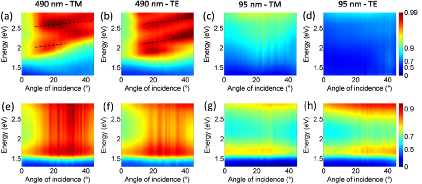
Figure 2. First row, transparent dielectric (PMMA)–Ag, and second row, organic semiconductor (PCPDTBT:PCBM)–Ag nanovoid interfaces. Absorption spectra are plotted with a logarithmic (base 10) color scale for incidence angles 0°–45°. The incident polarization and sample geometries are indicated for each column. Flat references are shown in the supplementary information (figure S1.2 available at stacks.iop.org/Nano/23/385202/mmedia). Prominent absorption features in (a) and (b) are marked with dashed lines.
Download figure:
Standard imageAn absorption feature for the transparent dielectric subwavelength-scale void sample appears at the upper energy limit of the measurement range (2.9 eV) (figures 2(c) and (d)). This feature is present for both TM and TE incident light, indicating that, like the wavelength-scale void sample, it is due to an LSP mode. This resonance is at the high-energy edge of the visible light region; no evidence of mode excitation is observed for the majority of the visible light and infra-red regions. The higher absorption of the transparent dielectric wavelength-scale sample (figures 2(a) and (b)) highlights the promise of LSPs with resonances within the visible photon energy range for optoelectronic applications.
We then compare these results with our imprinted nanovoid light trapping geometries, using a PCPDTBT:PCBM matrix with silver nanovoid interfaces (figures 2(e)–(h)). The real part of the composite refractive index of the PCPDTBT:PCBM material varies between 1.8 and 2 in the measured optical range and the absorption coefficient features a prominent dip between 2 and 2.5 eV (figure 3(a)) [25].

Figure 3. Organic semiconductor (PCPDTBT:PCBM)–Ag nanovoid interfaces. (a) Absorption of TM-polarized incident light for each of the sample geometries at 0° incidence (full lines) and the absorption coefficient of PCPDTBT:PCBM (dotted line). (b), (c) Relative enhancement in absorption (Astruc − Aflat)/Aflat for structured samples compared to the flat sample. The value of the enhancement is indicated by the (linear-scale) color bar.
Download figure:
Standard imageThe limited semiconductor absorption in the range 2–2.5 eV and below 1.5 eV is evident in the absorption spectra for the flat architecture (figures 3(a) and SI.2(c), (d) available at stacks.iop.org/Nano/23/385202/mmedia). We see that the absorption of the structured electrodes is significantly larger (figures 3(a) and 2(e)–(h)), especially in the 2–2.5 eV region. Similar to the transparent dielectric subwavelength-scale structure, an absorption enhancement feature is measured at the upper energy limit of the measurement range around 2.9 eV (figures 3(a), 2(g) and (h)). No strong dependence on incident polarization is observed.
Wavelength-scale voids exhibit stronger light trapping than their subwavelength counterparts (figures 2((e)–(h)) and 3), consistent with the transparent dielectric samples (figures 2(a)–(d)). At 0° incidence we observe total absorption enhancements (integrated over the energy range between 2.9 and 1.4 eV (430 and 880 nm)) of 40% and 20% for the wavelength- and subwavelength-scale voids respectively (figure 3(a)). Spectra of relative absorption enhancement ((Astruc − Aflat)/Aflat) do not display a strong angle dependence (figures 3(b) and (c))—the enhancement primarily occurs at energies where the OSC absorbs poorly (compare the absorption coefficient, figure 3(a)). In other words, the dispersive nature of the organic semiconductor, and not of the LSPs, dominates the spectra; the nanostructured electrode primarily boosts absorption of light at wavelengths where absorption is low. An important question is whether or not the absorption enhancement arises due to increased absorption in the organic film as desired. As mentioned earlier in this paper, all non-radiative dissipation of plasmonic modes must occur in the metal if the adjacent dielectric is non-absorbing. If the adjacent dielectric is an OSC, non-radiative dissipation of plasmon modes can occur via absorption in both the metal and the organic film. However, as a number of studies show, absorption in the OSC is strongly favored. The efficient dissipation of surface plasmon polariton mode energy into an organic film adjacent to a silver surface is known [6]. This is a direct consequence of the semiconductor's high absorption coefficient (see figure 3(a)) and low dielectric constant, which leads to a small overlap of the surface mode with the metal, thereby favoring absorption in the organic film. Efficient dissipation of localized mode energy into an OSC has also been calculated for organic films adjacent to silver void arrays similar to the ones used here, leading to large enhancements in the absorption of the organic film [14]. These studies are strong indications that the absorption enhancements observed here (figures 3(b) and (c)) arise primarily due to enhanced absorption in the organic film. Further evidence can be found from the newly emerging reports of solar cell efficiency enhancements obtained using metal nanostructures in organic solar cells [13, 26, 27].
An absorption feature is observed for the wavelength-scale structure at 2.5 eV at large angles (black arrow in figure 3(b)), which compares well with the wavelength-scale structure for the transparent dielectric film (figure 2(a) and (b)), although the feature is less pronounced and miniband dispersions are not resolved. This difference is attributed to absorption in the polymer (which has the effect of broadening the absorption features) and the truncated shape of the voids in the OSC sample. Previous studies have shown that the structure height of nanostructured metallic gratings has a strong influence on plasmonic resonances (both LSP and SPP) of the structure [22, 28]. Absorption of TE-polarized light (figure 2(e)) is similar to that of TM light (figure 2(f)), demonstrating the polarization-independent plasmonic enhancement. Simple finite element simulations [14, 15] of absorption in a planar architecture (figures SI.6, SI.7 available at stacks.iop.org/Nano/23/385202/mmedia) are used to demonstrate that the enhancement at 2.5 eV cannot be attributed to a Fabry–Pérot resonance for the modified OSC film thickness (125 nm for the truncated voids, figure 1(b) compared to 100 nm for the flat film) after imprinting.
A second absorption feature at around 1.45 eV (figure 3(b)) is also correlated with a dip in the absorption coefficient of the OSC. The subwavelength-scale structure (figure 3(c)) exhibits a somewhat smaller absorption enhancement—the enhanced absorption at 2–2.5 eV dominates the spectra.
4. Conclusion
In this work we have measured the angle-resolved specular reflectance spectra of imprinted nanovoid arrays. For samples featuring transparent dielectric–metal nanovoid interfaces we observe strong excitation of LSPs and evidence of plasmon–plasmon coupling for large structures (490 nm period) at visible wavelengths. We observe corresponding absorption enhancements in companion samples featuring OSC–metal nanovoid interfaces with evidence for LSP excitation in large structures (490 nm period). The absorption enhancement is found to be greatest at wavelengths where PCPDTBT:PCBM absorbs weakly. Nanostructured electrodes therefore have the potential to enhance solar cell performance by boosting absorption at wavelengths where it is most needed.
Acknowledgments
We gratefully acknowledge the IDK (Elite Network of Bavaria), the German research foundation DFG (SPP1355), the Nanosystems Initiative Munich (NIM) and UK EPSRC grants EP/G060649/1 and EP/F059396/1. We thank W Töllner and S Heiderich in the group of Professor Nielsch (University of Hamburg, Germany) for their support with AAO production.