
Abstract
The fabrication process and the operation characteristics of a fully roll-to-roll printed resistive write-once-read-many memory on a flexible substrate are presented. The low-voltage (<10 V) write operation of the memories from a high resistivity '0' state to a low resistivity '1' state is based on the rapid electrical sintering of bits containing silver nanoparticles. The bit ink is formulated by mixing two commercially available silver nanoparticle inks in order to tune the initial square resistance of the bits and to create a self-organized network of percolating paths. The electrical performance of the memories, including read and write characteristics, is described and the long-term stability of the less stable '0' state is studied in different environmental conditions. The memories can find use in low-cost mass printing applications.
Export citation and abstract BibTeX RIS
1. Introduction
The key drivers for printing as a fabrication method for flexible electronic components include: (1) the ability to cover large areas; (2) the ability to produce large quantities of products at low cost; and (3) as an additive fabrication method allowing lower material consumption with less waste when compared to subtractive fabrication methods [1]. Examples of devices and systems explored to be realized via printing of large active areas include solar cells [2], lighting panels based on organic light emitting diodes (OLEDs) [3], flexible active matrix displays [4], and electronic artificial skin [5]. Systems where large unit volumes are targeted with printing-enabled low manufacturing cost include radio frequency identification (RFID) tags [6], chemical sensors [7] and flexible power sources [8].
One key component required in most printed smart systems is the memory element [1]. To reach the markets, the printed memories should: (1) be printable in large volumes with high throughput methods and low cost; (2) be non-volatile with retention times exceeding months; (3) require low writing power, preferably within the range of printed power sources; (4) be at least write-once-read-many (WORM) type; (5) enable a straightforward read operation; and (6) enable integration for different processing methods and substrates to minimize the number of separately assembled components in the system.
Printable non-volatile memory elements whose active layers have been fabricated by solution processing can be divided into two main categories: (1) two-terminal resistance-change memories based on organic [9, 10], inorganic [11] or hybrid organic–inorganic [12] active layers; and (2) ferroelectric memory devices based on the ferroelectric polarization in capacitors [13–15], ferroelectric field-effect transistors (FeFETs) [15–17], and diodes [15]. In addition to FeFETs, also other types of three-terminal memory devices based on the controlled threshold-voltage shift in the gate transfer characteristics of printed thin film transistors (TFTs) have been reported [17]. Lately, also the overoxidation of poly(3,4-ethylene dioxythiophene):poly(styrene sulfonate) (PEDOT/PSS) in organic electrochemical transistors (ECTs) has been reported to induce a WORM effect [18]. However, the amount of reports on memories fabricated on flexible substrates solely by printing methods remains scarce thus far [13, 19, 20].
We have previously demonstrated [20–22] an ink-jet printed two-terminal resistive WORM memory on paper substrate that utilizes rapid electrical sintering (RES) of silver nanoparticles (NPs) for the low-voltage bit write process. In this paper, we show a fully roll-to-roll (R2R) printed resistive write-once-read-many (WORM) memory on a flexible low-cost plastic substrate. Also, we present a method for tuning the initial conductivity of the bits by mixing two commercial Ag NPs of different properties. When the mixed bit ink is gravure printed on a plastic substrate, a self-organized network is formed where the two ink components with differing encapsulants and average particle sizes remain in separated phases. The formed network enables percolation paths of low resistivity (larger particles) through the areas of higher resistivity (smaller particles with higher thermal stability due to more stable encapsulation)3. The WORM memories were printed both via sheet-fed and rotary direct gravure printing and rotary flexographic printing [23]. The memories are writable with low voltage (<10 V) and low power, they provide simple read and write operations and they show retention times exceeding months when stored in the dark with a desiccant. A simple electrical questionnaire card is presented as an example of memory integration.
2. Experimental methods
For the preparation of the NP bit ink, two commercially available high-viscosity Ag NP paste formulations were used: silver nanopaste DGP (denoted DGP from hereon) and silver nanopaste DGH (denoted DGH from hereon) by Advanced Nano Products Co. Ltd, Korea [24]. DGP is a low-temperature curing ink (120–150 °C, 30 min by manufacturer specification) with 60–80 wt% of Ag dispersed in α-Terpineol solvent and DGH is a high-temperature curing ink (230–300 °C, 30 min by manufacturer specification) with 65–80 wt% of Ag also dispersed in α-Terpineol solvent. The DGP/DGH mixture ink for tuning the bit ink properties was prepared by mixing the inks in different weight ratios while keeping the total mass fixed at 5 g. A small amount of toluene (0.2 g) was added to the mixture to lower the viscosity and to enhance the printability of the inks. Mixing of the inks was performed on a stirrer table followed by mixing in an ultrasonic bath.
The test structures for studying the properties of pure DGP and DGH pastes, DGP/DGH mixture ink and the bit writing with RES were printed using a table-top sheet-fed gravure Labratester printer (Norbert Schläfli Maschinen, Switzerland) on a 125 μm thick PET substrate (Melinex ST506). Dedicated printing plates were designed where the first plate contained laser engraved cups for printing of different sizes of WORM bits with nominal bit widths ranging between 15 and 100 μm and lengths between 0.1 and 0.5 mm. The bits were printed parallel to the printing direction. Resulting dried bits on the substrate were at maximum less than 30% wider than their nominal width. The second printing plate contained 'Xtreme' engraved cups for printing the contact electrodes aligned perpendicular to the bits. Printing parameters such as printing speed and nip pressure were optimized to obtain continuous printed structures and to avoid holes. The bits were printed as the first layer and the top contact electrodes were printed second with an ink containing micrometre sized Ag-flakes provided by Evonik GmbH. The layers were aligned manually by using printed alignment marks on both layers. After each layer, the samples were dried at 150 °C for 10 min. The contact electrodes showed a square resistance of approximately 1Ω/□ after drying.
The R2R printing of the WORM memories was performed using VTT's pilot R2R printing line 'ROKO'. The DGP/DGH mixture bit ink used in the R2R gravure printing run consisted of 54% of DGP (350 g) and 46% DGH (300 g) by weight. The viscosity of the ink was tuned with the addition of toluene (60 g) before mixing performed on a stirrer table and in an ultrasonic bath. The memories were fabricated on 125 μm thick heat stabilized PET substrate (Melinex ST506) using R2R direct gravure printing and specially designed printing rolls with laser engraved cups for the bit ink. The memory structure was printed using a continuous 5 m min−1 web flow from the input roll to the output roll with the following phases: (1) the bit layer was gravure printed using the developed DGP/DGH mixture ink; (2) drying inline in an oven at 140 °C for 25 s; (3) printing of the electrodes using Ag-microparticle ink (supplied by Evonik GmbH); (4) drying inline in an oven at 140 °C for 25 s. The registration between the adjacent layers was done with an inline camera system recording the alignment marks that were printed on the web alongside the first layer. A roll length of 150 m was printed containing more than 10 000 printed WORM memory banks. The printed output roll was transformed from the printing line to a R2R die cutter system for automatic separation of the individual memory banks from the roll. Some of the banks were manually hot laminated using a sheet-fed office laminator. The lamination was used to cover the bit area and approximately half of the contact electrodes, thus leaving an open contact electrode surface for physically contacting the bits.
The printing results were inspected using a standard optical microscope and the profiles of the printed structures were measured using a stylus profilometer (Dektak 150, Veeco Instruments). A typical bit height after printing and drying was approximately 600 nm. All scanning electron microscope images were obtained with a high resolution field emission SEM (LEO Supra 35 field emission SEM) with acceleration voltages below 10 kV to avoid charging of the insulating substrates.
Bit writing was performed with a circuit composed of a standard computer-controlled DC voltage supply and a rheostat connected in series with the bit. Gold-plated tungsten probes were used with manual micropositioners to contact the common electrode and the contact electrodes. The fast transition phase of bit writing was recorded using a standard digital oscilloscope. Details of the bit writing set-up can be found in [21].
The long-term retention measurements for the '0' state resistance of the table-top gravure printed memories were performed by measuring the resistance of the bits at the shown intervals. The bits were stored in the dark and were exposed to light and ambient humidity for a maximum of 5 min for each measurement point. The long-term retention time measurements for the '0' state resistance of the R2R produced memories were performed in the dark inside a climate chamber with separate temperature and humidity controls (Weiss WKL 34). The resistance was recorded at 30 s intervals with a standard computer-controlled multichannel digital multimeter using a low ( < μA) test current.
3. Results
3.1. Bit writing and readout methods
In printable metal-NP inks used for conductor fabrication, the NPs are typically encapsulated with ligands such as organic polymers or thiols to prevent agglomeration in the dispersion phase. After the deposition of the ink on a substrate, the ink solvents require evaporation which is typically achieved via mild thermal drying. After the printing and drying steps, the metallic NPs remain encapsulated and separated from each other with nanometre-range gaps. Depending on the NP packing density and encapsulation layer properties, only a limited conductivity occurs between the NPs due to inter-particle quantum-mechanical tunnelling and/or as leakage current e.g. via charge hopping through the encapsulation layer. The removal of the encapsulation layer is required to reach metallic conductance of the printed structures. Conventionally, the onset of metallic conductance can be achieved by heating the NPs over their curing temperature Tc [25], where Tc typically ranges from 150 °C up to several hundreds of degrees and is dependent on the properties of the encapsulation of the NPs [26]. A further increase in the conductance can be achieved via the sintering of the NPs, leading to coalescence and neck formation between the NPs. Alternatively to the thermal treatment, the NP structures can be sintered by applying a sufficient amount of energy in other forms via laser [27], intense pulsed light [28], electrical means (RF or DC) [21, 29–31], Ar-plasma [32] or by chemically removing the encapsulation of the particles [33]. These alternative curing methods target the lowered substrate thermal load as well as improved curing speed (critical in high-volume R2R processing).
The write operation of the WORM memory is in this paper based on RES of silver NPs. The principle of the RES process, described in more detail in [21, 30], is briefly as follows. By applying a voltage, a DC voltage in the case of the WORM memory in this paper, over a printed un-sintered structure, a non-vanishing tunnelling current and/or a leakage current through the encapsulation layers starts to flow between the separated particles. This causes Joule heating of the structure. When the heating power is large enough, the encapsulation melts/softens and the ligand is evaporated, removed or redistributed in the structure. This allows the reduction of the inter-particle distance and coalescence of particles driven by various mechanisms such as heat expansion, diffusion, inter-particle-force- or capillary-force-induced motion of the particles, and surface energy reduction [30, 35]. Consequently, as the electrical resistance decreases, more current will flow and more power will be absorbed, if a constant source voltage is applied over the WORM. Thus, the RES process has a strong positive feedback which results in fast sintering. By connecting a resistor in series with the sintered structure, both the peak power during the rapid (μs-range) transition and the current following the transition phase can be limited [21]. This allows in situ control of the final resistance after sintering.
The possibility to selectively and irreversibly modify the resistance of printed structures at a given time enables a memory write function which is utilized in this work. The printed WORM bits are initially at the high-resistance un-sintered '0' state and can be written to the low-resistance sintered '1' state with RES. The initial resistivity of the un-sintered bit ink determines the level of power absorption in the NP structure at a certain writing voltage. In other words, higher initial resistivity requires higher writing voltages to write the bits in a selected maximum writing time. The simplicity of the RES-based WORM memories consisting of printed metallic NPs distinguishes them from other printable resistance-change memories where the underlying reason for the resistance switching, in particular in re-writable resistance-change memories, is still not fully understood [9, 11, 12].
The readout of the presented resistive WORM memory can be performed both in contact and non-contact fashion. In contact readout, the bits are physically contacted and their resistance is measured e.g. with a reader device utilizing a low reading voltage [36]. Non-contact readout is based on a capacitive near-field measurement of the bit resistance with a sweep-over reader device [22]. The required ratio between the resistances of '0' and '1' states is specified by the accuracy of the reader device. The low-voltage writable WORM memories have been integrated in a number of printed electronics applications to provide small-scale memory operations [37].
3.2. Bit ink resistivity tuning with table-top gravure printed samples
The electrical properties of the bit ink were tuned by mixing two commercial Ag NP inks (by Advanced Nano Products Co. Ltd, Korea [24]) listed in table 1: DGP and DGH. According to the manufacturer's specification, the DGP ink has a low curing temperature of Tc,DGP = 120–150 °C, while the DGH ink has a high curing temperature of Tc,DGH > 230 °C. The average Ag particle sizes are 40–50 nm and 8–12 nm for the DGP and DGH inks, respectively. Previously, square resistances of ∼ 10 kΩ/□ and > 10 MΩ/□ were measured after printing and drying for the ink-jet printed formulations of DGP [21] and DGH inks [20], respectively. Both DGP and DGH inks have been successfully used as bit inks for WORM memories in their ink-jet printable formulations on photopaper substrates [20]. Preliminary tests were made with a table-top sheet-fed direct gravure printer for both pure DGP and DGH pastes diluted with toluene. The pure DGP ink was found to be writable with moderate electrical power, but exhibited insufficient environmental long-term stability manifested in the un-sintered '0' state resistance decrease, i.e. self-sintering, which can be due to the influence of temperature and moisture on the encapsulation of the particles. The pure DGH ink showed enhanced long-term stability, but required a high electrical power for sintering due to the high initial sheet resistance. Moreover, the DGH paste exhibited un-wanted spreading on plastic PET substrates, arising from both too low ink viscosity and the small nanoparticles slipping under the doctor blade of the gravure printer, as further discussed in section 3.3. Thus, neither the DGP or DGH ink was optimal for the memory bit realization as such.
Table 1. Bit ink component inks and their properties.
| Ag nanoparticle paste | Average particle diameter (nm)a | Curing temperature (°C)b | Un-sintered square resistance (Ω/□)c |
|---|---|---|---|
| Silver nanopaste DGP | 40–50 | 120–150 | ∼10 k |
| Silver nanopaste DGH | 8–12 | > 230 | >10 M |
aEstimated with a high resolution field emission SEM. bBy manufacturer specifications. cMeasured resistance of dry un-sintered films ink-jet printed on a photopaper substrate for DGP and DGH in [21] and [20], respectively.
In order to tune the initial resistance levels of printed bits, DGP and DGH pastes were mixed in various DGP/DGH compositions. Test samples were printed using a table-top sheet-fed gravure printer to study the initial resistance of the bits fabricated with different ink compositions. Figure 1 shows the initial sheet resistance of samples on PET substrate after printing and drying (at 150 °C for 10 min) as a function of the DGP percentage of the composition. Note that the drying temperature is high enough to induce sintering of the DGP ink. Four samples of each composition were measured and the error bars in figure 1 indicate the range of the measured values. The square resistance R□ drops monotonously from 10 MΩ/□ down to 100 kΩ/□ when the DGP content is increased from 50% to 75%. A further increase in the DGP content results in a rapid drop in R□ below 100 Ω/□. We associate this drop with the percolation onset, i.e. the formation of continuous low-resistance DGP paths through the sample. SEM images taken from the samples (figures 2(a)–(c)) reveal that the mixing of the component inks in the printed and dried samples is non-homogeneous. The larger DGP particles (bright areas of clearly resolved particles in figures 2(a) and (b)) and the smaller DGH particles (dark areas beyond SEM resolution at the used magnification in figures 2(a) and (b)) remain in separate phases and create a self-organized network structure on the substrate. This is highlighted in a lower magnification image (figure 2(d)). Figure 2(a) shows the ink with a 60% DGP percentage where the DGP content is too low to create continuous DGP paths, whereas in figure 2(b) the ink with a 70% DGP percentage shows already continuous DGP paths with an average network mesh size of ∼1 μm. However, a greater magnification image (figure 2(e)) taken from the same sample reveals that even in the DGP-rich areas, the larger DGP particles are surrounded by a halo of the smaller DGH particles. In contrast, in figure 2(c) where the DGP percentage is 80%, the DGP-rich areas are more abundant and the typical mesh size is significantly reduced. A greater magnification image (figure 2(f)) further shows that now only a few smaller DGH particles are gathered around the larger DGP particles in these areas.
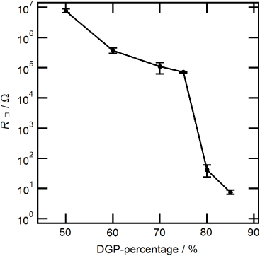
Figure 1. Square resistance R□ of table-top gravure printed and dried bits on a plastic substrate as a function of DGP percentage.
Download figure:
Standard image
Figure 2. SEM images of mixed inks with varied DGP percentage of (a) 60%, (b) 70% and (c) 80%. (d) Zoomed out view of ink with a DGP percentage of 70%. Close-up high resolution SEM images of the DGP-rich areas for mixed inks with a DGP ratio of (e) 70% and (f) 80%.
Download figure:
Standard image3.2.1. Bit writing tests with RES.
Bit writing tests with RES were made for samples printed with a mixed DGP/DGH ink having a 70% DGP percentage. This DGP content was selected as it produced a suitable combination of continuous DGP paths and still sufficiently high initial sheet resistance R□ > 1 kΩ for good long-term stability. The details of the bit writing set-up are described in section 2. Bit writing was performed, for example, using a low writing voltage of Uwrite = 10 V for bits of length L = 290 μm and width W = 120 μm. A series resistor Rs = 340 Ω was used to limit the maximum current to comply with a typical maximum output current of printed batteries (tens of milliamps). Figure 3(a) shows the characteristics of the bit writing process with the bit resistance and the dissipated power as a function of time. The bit resistance drops from R'0' = 4.7 kΩ below R'1' < 100Ω in writing time twrite = 11 ms, which is denoted as the time between switching on the writing voltage and the point where the fast transition from the '0' state to '1' has occurred. The writing time twrite is shown in figure 3(a) as a dashed blue arrow.

Figure 3. Characteristics of table-top gravure printed WORM bits. (a) Bit writing from the high-resistance '0' state to the low-resistance '1' state: bit resistance Rbit (red curve, left axis) and dissipated power Pbit (black curve, right axis) as a function of time t. The writing time twrite of the bits is shown. (b) Long-term retention measurement for three samples stored in the dark at ambient conditions (20 °C < T < 25 °C and 10% < RH < 30%) inside a plastic sleeve with a desiccant. The '0' state bit resistance Rbit is shown as a function of storage time t.
Download figure:
Standard image3.2.2. Long-term stability.
The long-term stability of the '0' state resistance was previously found to be affected by moisture and temperature with ink-jet printed WORM bits compromising both DGP and DGH inks [20]. As the written '1' state of the bits was found to be stable in ambient conditions, it was of interest to monitor the stability of the '0' state resistance of the bits gravure printed with the mixed DGP/DGH ink. Figure 3(b) shows the '0' state resistance as a function of time for three samples stored in the dark at ambient room conditions (20 °C < T < 25 °C and 10% < RH < 30%) inside a plastic sleeve accompanied by a piece of cleanroom paper sheet as a desiccant. An onset of slow decline in the resistance can be observed after storage of approximately four months. Overall, the bits show good '0' state stability during 19 months of monitoring time.
3.3. Roll-to-roll produced WORM memories
After the successful tuning of the initial '0' state resistance with table-top gravure printed devices, R2R direct gravure printing was used to demonstrate the mass-production feasibility of the memories. Figure 4(a) depicts schematically the R2R printing process. The DGP/DGH composition was adjusted based on R2R test runs to 54% DGP content which was found to yield the desired initial resistance levels in the R2R conditions. The different optimum composition as compared to table-top experiments discussed above can be due to differences in (1) the ink transfer (table-top plate gravure versus R2R gravure cylinders); (2) control of the drying process; or (3) ink chemistry in larger volumes at the R2R line.
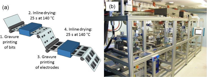
Figure 4. (a) Schematic image of the R2R gravure printing process steps. After the R2R printing line, the printed roll containing the WORM memory banks is fed into a separate R2R die cutter. Some of the cut WORM memory banks are laminated with a sheet-fed laminator. (b) VTT's R2R printing line 'ROKO' was used in this work.
Download figure:
Standard imageThe layout of the R2R multi-bit WORM banks is shown in figure 5. The comb-shaped device consists of the common electrode, the separate electrodes for each bit, and the actual bits spanning the electrode gap. Several different bit sizes were fabricated in order to study and to optimize the electrical properties of the bits: length L = 100, 200, 300 and 400 μm and width W = 100,200,400 and 800 μm. Also, memory banks of different bit densities (pitch 1, 2, and 4 mm) were fabricated. After printing and drying, the average sheet resistance of the contact electrodes and the common electrode printed with Ag-flake ink was sufficiently low (less than 1 Ω/□). The resistance of the pristine bits after printing and drying ranged from several MΩ to less than 1 kΩ depending on the bit size.
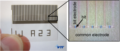
Figure 5. Photograph of a printed WORM memory bank with 26 bits (1 mm pitch) with contact electrodes and a common electrode. Right: an optical microscope image of the bit layout. The bit size is approximately W = 200 μm and L = 300 μm.
Download figure:
Standard image3.3.1. Bit writing characteristics.
Figure 6(a) shows an optical microscope image a WORM bit of size L = 200 μm and W = 200 μm before (at the left) and after (at the right) bit writing. The bit writing process causes a rapid filamentary path formation through the percolating DGP network in the bit which is seen in detail from the SEM images shown in figure 6(b). The path width was observed to be constantly approximately 10 μm with different sintering peak powers Pmax. The insets in figure 6(b) show the particle size outside the path (top inset) and inside the path (lower inset), indicating a significant grain growth in the low-resistance percolation path due to RES and highlighting the irreversibility of the write process. Similar initial filamentary path formation has been previously recorded with fast IR-camera reflectivity measurements for ink-jet printed homogeneous DGP ink structures contacted with sharp tungsten probe needles [34].
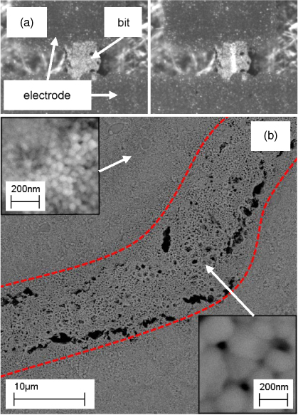
Figure 6. (a) Optical microscope image of a single WORM bit before (left) and after (right) writing. After bit writing, a sintered path is visible. (b) SEM image of a written bit with the sintered path marked with red dashed lines. Top inset: high magnification image from outside the path with un-sintered particles. Bottom inset: high magnification image from inside the path showing significantly increased grain size.
Download figure:
Standard imageThe writing characteristics of a bit of size L = 200 μm and W = 200 μm are shown in figure 7(a). The writing voltage was Uwrite = 8 V and the current limiting series resistor was set to Rs = 250 Ω. The resistance of the bit drops over a decade during the bit writing process from R'0' ≈ 1.4 kΩ to R'1' < 100 Ω in twrite ≈ 5 ms. A collection of the writing characteristics for a batch of similar sized bits is shown in figure 7(b). The writing time twrite is shown as a function of the initial '0' state resistance R'0' for four bit writing voltages ranging from 3 to 15 V. Qualitatively, as Uwrite was increased, twrite was reduced for bits of similar R'0'. Similarly, for a fixed twrite, Uwrite could be lowered by using bits with lower R'0'. To limit the current through the bits after writing, the series resistance Rs was selected such that Rs < 2R'0'. Figure 7(b) is divided in three areas on the basis of the resistance ratio R'0'/R'1' between the '0' and '1' states for written bits. The resistance ratio corresponds to R'0'/R'1' < 50 in area I, to 50 < R'0'/R'1' < 100 in area II, and to R'0'/R'1' > 100 in area III. The readout method determines the required resistance ratio. For example, if R'0'/R'1' > 100 is required, based on figure 7(b), it takes several seconds to write the bit using a 5 V voltage, while using a 15 V voltage the writing can be done in a few milliseconds.
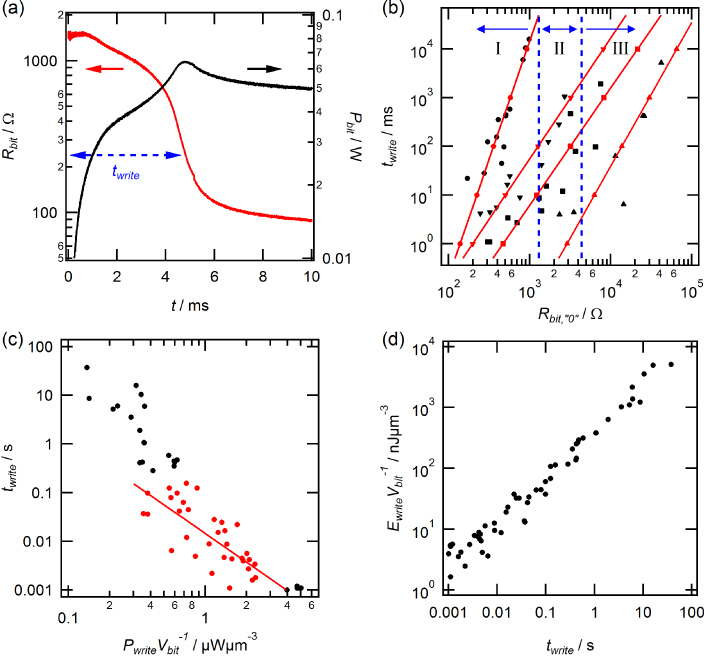
Figure 7. Bit writing characteristics for R2R produced WORM bits of 200 μm × 200 μm size. (a) Bit writing from the high-resistance '0' state to the low-resistance '1' state: bit resistance Rbit (red curve, left axis) and dissipated power Pbit (black curve, right axis) as a function of time t. The writing time twrite of the bits is shown. (b) Writing time as a function of the initial '0' state resistance for samples written with (•) 3 V, (▾) 5 V, (▪) 8 V, and (▴) 15 V. The red lines show curve fits. On the basis of the resistance R'0'/R'1'-ratio for written bits, the graph is divided into three regions: R'0'/R'1' < 50 in I, 50 < R'0'/R'1' < 100 in II, and R'0'/R'1' > 100 in III. (c) Writing time twrite as a function of applied power density  . The red points (1 ms < twrite < 100 ms) were included in a linear fit which corresponds approximately to the temperature rise to Tc ≈ 180 °C before the fast transition phase calculated using the one-dimensional heat-conduction model presented in [30]. (d) Energy density
  as a function of writing time twrite.
Download figure:
Standard imageFigure 7(c) shows the bit writing time twrite as a function of the applied power density  , where Vbit denotes the bit volume. The used voltage supply had a finite rise time for reaching the set voltage and, therefore, the minimum writing time was limited to approximately 1 ms. As the writing power density was increased, the bits were written faster and the relation followed approximately a linear dependence on a logarithmic scale as quantitatively predicted based on the heat transfer dynamics in the electrical sintering process for writing times below 100 ms [30]. A linear fit is shown for the data points with 1 ms < twrite < 100 ms (shown as red points). By using a one-dimensional heat-conduction model, as presented in [30], for estimating the bit temperature prior to the fast transition phase, the fitted line corresponds to a transition temperature of Tc ≈ 180 °C (see supporting information S1 available at stacks.iop.org/Nano/23/305204/mmedia). The estimated Tc for the bits containing the mixed DGP/DGH ink is higher than the curing temperature for pure DGP particles (Tc,DGP = 120–150 °C), but significantly lower than for pure DGH particles (Tc,DGH > 230 °C). Figure 7(d) shows the calculated energy density
  as a function of the bit writing time twrite. The minimum energy density of ∼2 nJ μm−3 was calculated for the measured writing time of ∼1 ms. Similar minimum writing energy density values were reported earlier for ink-jet printed WORM memories [20].
As already seen in figure 7(b), the initial '0' state resistance R'0' has a very high variation among the bits of similar size. This leads to a variation in the writing characteristics, since twrite is determined by both Uwrite and R'0'. Figure 8(a) shows that the large variation is observed both in the average initial resistance between the memory banks of similar bit size and also between the bits of the same memory bank. A likely reason behind the high variation is the open ink vessel used in the printing equipment: the ink composition did not remain constant due to solvent evaporation. To exclude geometrical reasons behind the variations, the bit geometries were measured with an optical microscope and a stylus profilometer. No clear correlation between the resistance and the cross-sectional area of the bits was found. Furthermore, in a SEM investigation, no difference in the microstructure of the bits was visible. It should also be noted that although the memory bits are several orders of magnitude larger than the nanoparticle dimensions, averaging out of the randomness of the particle structure can be limited along the narrow DGP particle percolating paths.
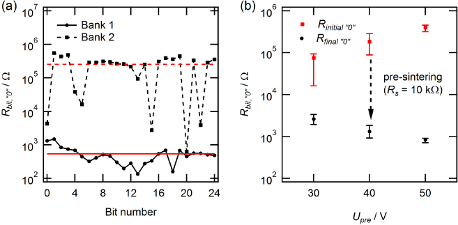
Figure 8. (a) The initial bit '0' state resistance Rbit,'0' of two WORM memory banks of equally sized bits. The red lines show the average resistance of bits for each bank. (b) Bit resistance Rbit as a function of pre-sintering voltage Upre. Pre-sintering with high voltage can be utilized to equalize the initial '0' state resistance to a constant low level of ∼1 kΩ. The red dots denote the initial bit '0' state resistance Rinitial'0' and the black the final bit '0' state resistance Rfinal'0' after pre-sintering. A high limiting series resistance of Rs = 10 kΩ was used.
Download figure:
Standard imageIn order to deal with the resistance scatter, electrical pre-sintering of the bits can be utilized. By tuning the series resistor of the bit writing set-up, the maximum current and power can be limited and the end resistance of the structures can be controlled reliably [21, 36]. By using a high series resistance of Rs = 10 kΩ, one can electrically pre-sinter the bits to have nearly uniform resistance in the order of 1 kΩ. This is shown in figure 8(b) for samples with a high initial resistance treated with different pre-sintering voltages. Electrically pre-sintered samples were further written into the '1' state with a low writing voltage (Uwrite < 10 V).
3.3.2. Long-term stability of the bits.
Long-term stability measurements of the unwritten '0' state resistance R'0' were performed on R2R printed WORM memory banks that were manually hot laminated. Instead of storage at room conditions, the retention tests for the R2R produced memories were performed as accelerated lifetime tests either with elevated temperature T and/or with elevated relative humidity (RH). All stability tests were performed in a darkened climate chamber. Figure 9(a) shows the relative bit resistance Rbit(t)/Rbit(t = 0) as a function of the exposure time t for samples kept in different conditions: (1) T = 20 °C, RH = 50%; (2) T = 50 °C, RH = 20%; (3) T = 50 °C, RH = 50%; and (4) T = 85 °C, RH = 85%. The solid lines denote the average of n > 20 bits for each sample set and the dashed lines denote the standard deviation. The measurements show a clear dependence on both moisture and temperature. The bits exposed to elevated humidity levels of RH = 50% but kept at a low temperature of T = 20 °C (black curve) show only a slight (<10%) or no decrease of R'0' during one week of monitoring. When the temperature is increased to T = 50 °C while the humidity is kept at RH = 50% (blue curve), a fast degradation is observed with the majority of the bits exceeding ∼80% drop in R'0' in one week. However, an elevated temperature of T = 50 °C combined with a low humidity RH = 20% (red curve) causes only a drop of ∼30% in R'0' during the same time. Extreme conditions such as a high temperature of T = 85 °C combined with a high humidity of RH = 85% (red curve) cause a rapid drop below 10% of the initial R'0' in less than 3 h.
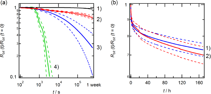
Figure 9. Long-term stability measurement for R2R produced and manually laminated WORM banks stored at different atmospheric conditions. (a) Relative bit resistance Rbit(t)/Rbit(t = 0) as a function of exposure time t for samples stored at: (1) T = 20 °C, RH = 50% black curve; (2) T = 50 °C, RH = 20% red curve; (3) T = 50 °C, RH = 50% blue curve; and (4) T = 85 °C, RH = 85% green curve. (b) Relative bit resistance as a function of exposure time for (1) pre-sintered (blue) and (2) unmodified (red) samples.
Download figure:
Standard imagePreviously described electrical pre-sintering could affect the stability of the pre-sintered '0' state resistance R'0' by removing the encapsulation of a fraction of the particles of the bit. Therefore, some bits were pre-sintered with Upre = 18 V and Rs = 10 kΩ in the WORM bank which was exposed to an elevated temperature of T = 50 °C and a low humidity of RH = 20%. Figure 9(b), however, shows no clear difference in the decay of the relative bit resistance between the pre-sintered (blue) and the unmodified (red) bits.
3.3.3. Flexographic printing of WORM memories.
In gravure printing, the doctor blading was found to be problematic with the nanoparticle inks. Nanoparticles (d < 50 nm) can slip under the doctor blade due to the deliberate finite roughness of the printing plate (in table-top gravure) or cylinder (in R2R gravure) used to lubricate the doctor blade and sharpen the printing result. This gives rise to parasitic ink residual in the non-image areas as can be seen from a SEM image taken outside the bit area (see figure 1S(a) in the supporting information available at stacks.iop.org/Nano/23/305204/mmedia). Both the sheet-fed and R2R gravure printed samples exhibited debris on the substrate that was visible to the naked eye as a transparent reddish colour and further identified under SEM as separated DGP and DGH particles. However, the debris was non-conducting and did not affect the electronic properties of the printed memory devices.
To avoid the particle slipping problem, R2R flexographic printing was investigated [23]. No ink debris was seen on the substrate with flexographic printed bits (see figure 1S(b) in the supporting information available at stacks.iop.org/Nano/23/305204/mmedia). The bit writing performance was similar to that with R2R gravure printed bits.
3.4. Roll-to-roll produced WORM memory applications
Currently, the research of printed memories is directed towards re-writable memories as they enable devices of higher complexity and logic (e.g. book-keeping capability) when compared to WORM memories. However, the resistive WORM memory enables simple read and write operations when compared to destructive readout of ferroelectric capacitor memories [15]. The low-voltage writable WORM memories presented in this paper can provide simple memory functions for several types of printed electronics applications ranging from programmable RFID tags to data-logging applications where sensor or user input data are stored for later readout. Both fully printed and hybrid Si-chip-integrated application demonstrators have been previously presented [37, 38].
Figure 10(a) shows an example of a printed system demonstrator utilizing the developed WORM memory. The electrical enquiry card contained a 12-bit WORM bank and a thin battery by Enfucell Ltd; the WORM memory was used to store the user push button presses. A batch of 1000 cards was manufactured and used at the Printed Electronics Europe 2011 conference (vote for the best booth at the conference) [39]. The WORM memory banks compromising electrically writable Ag nanoparticle bits were printed with R2R flexographic printing as shown in figure 10(b). The write voltage for the WORM memories was supplied by flexible printed batteries [40]. A Si-based light-emitting-diode (LED) was embedded in the system to indicate a successful push button action. Automatic computer-controlled pre-sintering of the memory bits to a suitable initial resistance level of < 1 kΩ and the readout of the memory banks were performed using the device shown in figure 10(c). The device consisted of an array of spring-loaded probes to contact the electrodes at the top of the card shown in figure 10(a).
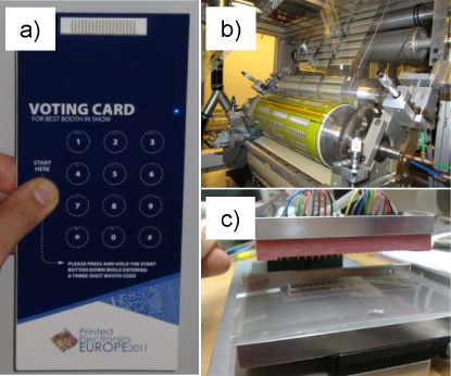
Figure 10. (a) A printed questionnaire card with a R2R printed 12-bit WORM memory bank, flexible battery and a Si-based light-emitting-diode assembled together as a system. The graphical printing, screen printing of electrical wiring with a conductive silver ink and the card assembly were performed at Stora Enso Oyj. (b) R2R flexographic printing of WORM memory banks for the questionnaire card with VTT's 'ROKO' printing line. (c) WORM memory bank pre-sintering and the readout device. The electrical contacts were realized using an array of spring-loaded probes.
Download figure:
Standard image4. Discussion
In this paper, we demonstrated a method to tune the initial un-sintered state resistance of printed structures on plastic PET substrate via the mixing of two metallic NP inks. Previously, it has been shown that by mixing ligand-capped small diameter (d < 5 nm) Au NPs and conducting polymers, such as PEDOT/PSS, the final sintered resistance of homogeneous composite films can be controlled via changing the Au NP and polymer weight ratio [41].
The printed mixed bit ink created a self-organized network on the substrate surface where the two particle size distributions were kept mainly in separate phases. The DGP and DGH particles of the mixed ink show clearly a size-induced segregation. The spontaneous ordering of the dried NP dispersions with bimodal or polymodal size distributions has been previously studied e.g. for thiol-stabilized gold NPs [42]. However, the observed size segregation of dried films can also arise from non-homogeneous mixing of the polar and non-polar components of the bit ink already in the dispersed phase. Ultimately, the exact mechanism leading to the observed self-aligned network is outside the scope of this study.
The advantages of the observed non-homogeneous ink mixing are: (1) tuning the initial conductivity of dried films by simply changing the weight ratio of the two NP ink components; (2) the mixing provides a well-controllable (nearly linear) conductivity tuning, whereas changing the thickness of the encapsulation of the metallic NPs results in an exponential change in the resistance (the tunnelling resistance between the particles); (3) the percolation network via the threads of the larger particle material promotes a filamentary path (10 μm wide seen in the tests) formation. The filament formation reduces the required writing power as the entire bit volume is not required to be sintered. Furthermore, as the electrical writing properties are then not determined only by the size of the bits, the filament formation also enables the use of a coarse printing resolution with large-volume printing methods; and (4) the method provides a desired compromise in bit performance (increased the long-term stability combined with the ease of write performance) when compared to bits printed with either of the component inks. The presented mixing method to tune the initial resistivity of printed NP structures via the creation of percolating low-resistance networks can be generalized to govern also semiconducting or insulating materials that mix in a similar non-homogeneous way.
With the separate galvanic readout contact for each bit, the memories consume a single physical contact for each bit, which limits the total memory capacity. On the other hand, the electrical write process provides the possibility to easily control the programmed resistance; this can be done, for example, by changing the series resistor Rs. Thus, a multi-level (stair-case-type resistance pattern) operation of the WORM memories is enabled and the overall memory capacity can be significantly increased (more storage for each physical bit) [10]. Also, the multi-level programming could be used as an analogue memory to store data obtained e.g. from a printed sensor. Ultimately, the total amount of available levels is determined by: (1) the accuracy of distinguishing between adjacent levels; (2) the programming accuracy (the variation in the resistance between devices written to the same state); and (3) the long-term drift in the resistance levels.
Reducing the amount of physical contacts and higher memory capacities could also be obtained by implementing a memory addressing logic by combining WORM bits either in series with rectifying diodes (1D-1R) [43] or with bits addressing transistors (1T-1R) [44] in a memory cell matrix. However, for the write operation, this would require either a very high on-state current carrying ability (tens of milliamps) coupled with low operating voltages ( < 10 V) for the transistors or a high rectifying ratio coupled with a high forward current density for the diodes to prevent sneak current paths. Both are still high demands for the current state of the art printed semiconductor components.
The long-term environmental stability of the '0' state resistance of the bits could be increased with a more advanced device encapsulation. The performed hot lamination did not form a full hermetic barrier as the moisture was allowed to be absorbed in the open area of the microporous Ag electrodes and further diffuse to the NP bits. Further device encapsulation tests are thus required in order to estimate the shelf time of the memories. Possible solutions to improve the stability of the '0' state resistance include: (1) a full device encapsulation with lamination; (2) printed lamination layers over the bits; or (3) encapsulated desiccant in the bit vicinity.
5. Conclusions
We have demonstrated fully R2R gravure and R2R flexographic printed resistive WORM memory devices based on Ag NPs on a flexible substrate. The low-voltage write operation utilizes the RES process and the read operation can be performed both via capacitive (non-contact) or resistive (contact) measurement. The bit ink properties, including the initial '0' state resistance, were tailored by mixing two different commercial Ag NP pastes in different weight ratios. The resulting printed and dried layers exhibited size segregation of the two ink component NPs, leading to a self-aligned network of low-resistance percolation paths. The observed high variation in the '0' state resistance of the bits can be controlled by pre-sintering the bits to a constant level. The memories show excellent '0' state retention of over 19 months when stored in the dark with a desiccant. However, both elevated temperature and moisture were found to rapidly decrease the '0' state resistance of laminated devices. The WORM memories can find usage in various printed low-cost applications. A simple electrical questionnaire card was presented as an example.
Acknowledgments
The authors gratefully acknowledge the valuable discussions with Dr Changwoo Park of Advanced Nano Products Co. Ltd. Mr Simo Siitonen of Stora Enso Oyj is gratefully acknowledged for the questionnaire card work. Enfucell Ltd is acknowledged for the flexible batteries. Mr Janne Raappana, Mr Pekka Ontero and Mr Arto Ranta-Panula are acknowledged for the printing work at VTT. This work was supported by the European Community's Seventh Framework Program FP7/2007-2013 under Grant 215132 (project PriMeBits).
Footnotes
- 3
Particles with a smaller diameter d have a larger amount of tunnelling contacts per unit length in tandem with smaller capacitance when compared to particles with a larger d.