Abstract
We report a systematic study of Si|ZnO and Si|ZnO| metal photocathodes for effective photoelectrochemical cells and hydrogen generation. Both ZnO nanocrystalline thin films and vertical nanowire arrays were studied. Si|ZnO electrodes showed increased cathodic photocurrents due to improved charge separation by the formation of a p/n junction, and Si|ZnO:Al (n+-ZnO) and Si|ZnO(N2) (thin films prepared in N2/Ar gas) lead to a further increase in cathodic photocurrents. Si|ZnONW (nanowire array) photocathodes dramatically increased the photocurrents and thus photoelectrochemical conversion efficiency due to the enhanced light absorption and enlarged surface area. The ZnO film thickness and ZnO nanowire length were important to the enhancements. A thin metal coating on ZnO showed increased photocurrent due to a catalyzed hydrogen evolution reaction and Ni metal showed comparable catalytic activities to those of Pt and Pd. Moreover, photoelectrochemical instability of Si|ZnO electrodes was minimized by metal co-catalysts. Our results indicate that the metal and ZnO on p-type Si serve as co-catalysts for photoelectrochemical water splitting, which can provide a possible low-cost and scalable method to fabricate high efficiency photocathodes for practical applications in clean solar energy harvesting.
Export citation and abstract BibTeX RIS
1. Introduction
After the idea of photoelectrolysis (solar-energy-assisted water splitting process) using a semiconductor electrode was introduced by Fujishima in 1972 [1], lots of research has been done, particularly in the past two decades, to search for a sustainable electrode material for photoelectrolysis (the device used for photoelectrolysis is well known as a photoelectrochemical cell or PEC cell), which is believed to be the essential approach to the clean H2 economy. A photocathode is one of the electrodes for photoelectrolysis supplying photogenerated electrons to react with protons from the electrolyte and directly generate H2 gas. An appropriate photocathode material should have band bending favorable for transfer of photogenerated electrons to the solid/solution interface, which requires the conduction band edge to be more negative than the H2/H+ redox potential, the Fermi level to be more positive than the H2/H+ redox potential, and for electrons to be the minority carriers. P-type Si meets these requirements and is one candidate photocathode material. Moreover, Si is abundant and cheap, and has a small bandgap (1.12 eV), which is good in terms of having a broad absorption coverage of the solar spectrum.
Surface kinetics is a very important parameter determining device performance, particularly for Si. Si shows extremely low surface kinetics leading to a competing process of recombination at an interface to an aqueous solution where band bending is minimal [2–6]. This is the result of a large number of surface states which cause 'Fermi level pinning' at the surface of the electrode, forcing band bending independent of the redox level of the solution.
However, studies of p-Si photoelectrodes also showed some problems, such as (i) the band alignment between Si and water redox levels does not allow spontaneous water splitting without an external bias and (ii) more seriously, Si is not chemically stable and photodecomposes (Si is particularly unstable under anodic bias). There is no single material that can meet all the criteria for photocathode selection and nature tends to be lacking in other choices of low-cost and stable p-type materials for photocathodes [7]. One possible approach is to integrate different materials to form a heterogeneous system with more desirable properties. Recent studies on coating an n+-layer onto a p-type Si surface has shown to reduce the external bias due to the additional photovoltage generated at the n+/p junction [8, 9]. Various metals in the form of particles or thin films deposited on the semiconductor photoelectrode surface are used to improve the catalytic activity. However, this metal|semiconductor structure is recognized to contribute to a large decrease in photovoltage because the metal coating promotes carrier recombination at the surface and decreases surface band bending [10].
In this paper, we report metal and metal oxide co-catalyzed p-type Si-based photocathodes, where an n-type wide bandgap metal oxide layer is sandwiched between the metal layer and p-Si. This structure allows enhanced charge separation and transport of photo-induced electrons from p-type Si to n-type metal oxide due to the internal p/n junction and band bending, as well as improved carrier travel across the metal oxide (electrons are majority carriers) to the electrolyte/electrode interface. Furthermore, a nanostructured metal oxide layer can improve the overall effective surface area for the chemical reaction, thus improving the cathodic photocurrent density. The metal thin film coating on metal oxide nanowire surfaces offer catalysis and protection to the heterostructure photocathodes.
2. Experimental procedures
2.1. Si wafer cleaning
Boron-doped prime grade p-type (100) Si wafers (1–10 Ω cm, University Wafer) were initially cleaned with a standard solvent cleaning process. Wafers were then dried with a stream of N2 gas and immediately transferred to the sputtering deposition chamber avoiding further oxidation.
2.2. ZnO seeding layer coating and ZnO nanowire growth
A thin layer of different seeding materials was then deposited on the polished side of the wafer through magnetron RF sputtering. Normally argon gas was used to ignite the plasma. A mixed Ar with 10% N2 was also used during ZnO sputtering. Deposition was conducted without substrate heating or RF bias. Different seeding materials used for investigation include 99.99% ZnO sputtered in Ar, labeled as ZnO(Ar), in mixed Ar/10% N2, labeled as ZnO(N2), and 2% Al2O3-doped ZnO sputtered in Ar, labeled as ZnO:Al. The deposition rate was kept at a constant value of 3 nm min−1 and thickness of the seeding layer was varied from 25 to 170 nm. During deposition, sputtering power was fixed at 200 W with a constant gas flow rate of 30 sccm. Working pressure was kept at no higher than 1.9 mTorr at room temperature.
Seeded Si wafers were then diced into 6.35 × 6.35 cm2 and stored under vacuum for further processing. To grow ZnO nanowires using a solution-based method, a solution of 0.25 M hexamethylenetetramine (HMTA, sigma) and the same concentration of zinc acetate (Zn(AC)2, Sigma) was made in the reaction container (three-necked flask). Diced samples were then fixed on supporting glass slides face down and carefully transferred to the flask. The flask was purged with N2 and immersed in the oil bath during growth. Growth was carried out at 90 °C. The growth timer was started once the solution temperature reached 60 °C. Samples were grown for various times from 10 min to 2 h. The samples were rinsed with DI water (17.6 M Ω cm) immediately after being taken out of the reaction solution. Gentle sonication was then used to remove surface particle residuals and the samples were then blown dry with a stream of N2.
2.3. Metal catalyst deposition
Gas phase deposition of metal catalysts was realized using electron-beam evaporation at a base pressure of 8 × 10⁻⁷ Torr. The metal coating thickness was monitored by the quartz resonator. 5 nm of Pt, Pd and Ni was evaporated onto the various samples (plain Si, ZnO thin-film-coated Si and ZnO nanowire-coated Si).
2.4. Surface morphology analysis
A scanning electron microscope (SEM, Philips XL30 ESEM) equipped with a field emission gun and an energy dispersive spectroscopy (EDX) detector was used to investigate the surface morphology and chemical composition. A tapping-mode atomic force microscope (AFM, Veeco scanning probe microscope) equipped with a standard silicon probe (Umasch NSC15/no Al) was also used to evaluate the surface nanoscale topological differences between the thin film coatings. Raw data collected by AFM were processed using NanoScope software; surface roughness and grain size were obtained using NanoScope Analysis software.
2.5. Hall measurement
The resistivity and carrier concentration of the sputtered ZnO thin films were tested using a home-built Hall measurement set-up.
2.6. Electrode and electrolyte solution preparation
The backsides of the Si samples were gently scratched and Ga/In eutectic alloy was applied to produce an ohmic contact between an insulated copper wire and the Si sample. The edges and backside of the samples were protected by epoxy to isolate them from contacting the electrolyte (figure 1(a)). Areas of epoxy-protected samples in contact with the electrolyte were calculated using image processing. All the electrochemical experiments were carried out in a PBS buffered 0.25 M sodium sulfate (Na2SO4 pH = 7.2) at room temperature. The pH was measured and monitored using a pH5 pH meter (Acorn, Oakton).

Figure 1. (a) Schematics (left) and optical image (right) of prepared sample electrodes and (b) schematics of PEC measurement set-up.
Download figure:
Standard image2.7. Photoelectrochemical measurement
In all the electrochemical measurements, a single cell and three-electrode set-up was used. The three electrodes consisted of a Pt mesh counter electrode (CE), Ag/AgCl reference electrode in 1 M KCl (RE) and the sample as a working electrode (WE). The measurement set-up is shown in figure 1(b). All of the electrodes were kept as close as possible and their position kept constant for every sample. A xenon lamp solar simulator (UV-enhanced, Newport) with 1.5AM filter was used as a light source. Distance from sample to the solar simulator was 22 cm which provided a constant power density of 100 mW cm−2 at the sample position. Power intensity and spectrum at this particular position was initially calibrated for a more accurate estimation of the efficiency and spectrum response. Irradiation was applied perpendicularly to the sample surface through a quartz window to minimize spectrum loss. A magnetic stir bar was employed to agitate the electrolyte, to remove bubbles at the sample surface and to further minimize the thickness of the diffusion layer on the electrode surface, which could introduce error into the measured current density. An inert gas purge using N2 was applied prior to each measurement for at least 5 min to remove dissolved O2 and mainly CO2 in the electrolyte. This served to minimize the effect of these dissolved gases. Samples were stabilized in the electrolyte after each scan by monitoring the open circuit voltage for at least 10 min. During measurement the N2 purge was kept running to maintain a N2 saturation environment at the electrolyte/air interface. A potentiostat (DY2322, Digi-Ivy) was employed for the data collection.
3. Results and discussions
Figure 2 summarizes the structures of the photoelectrodes studied in this paper, where figures 2(a)–(c) show the schematic of the photoelectrodes of planar p-Si, n- or n+-doped metal oxide thin-film-coated p-Si (n/p junction) and ZnO nanowire-coated n/n+-ZnO/Si, respectively. Figures 2(d)–(f) show the energy band diagrams. Metal thin films were also coated on the three kinds of photoelectrodes, particularly as co-catalysts with the oxide or oxide nanowires, which were not shown in figure 2.

Figure 2. Schematics of photocathode structure: (a) bare planar p-Si, (b) p-Si|n/n+-ZnO and (c) p-Si|n/n+-ZnO|ZnO nanowires. Energy band diagram at equilibrium: (d) bare p-Si with Fermi level pinning, (e) p-Si|n-ZnO|ZnO nanowires and (f) p-Si|n+-ZnO|ZnO nanowires.
Download figure:
Standard imageFrom the theoretical design point of view, a single-material electrode using Si alone offers limited photocurrent and low H2 evolution kinetics, which is due to the competitive carrier recombination process (figure 2(a)) particularly when the band bending at the interface is small (figure 2(d)). Generally, this is true for Si where the Fermi level is pinned at the surface, without considering the energy distribution of the surface states or the large density of surface states [11, 12]. The pinned Fermi level results in the change of applied potential in the Helmholtz layer instead of the space charge region [3]. Unlike the single-material system, a binary system using n-type ZnO on p-type Si (figures 2(b) and (c)) forms a p/n junction between the materials, which can provide an effective electric field to separate the photogenerated carriers, minimizing carrier recombination in Si (figures 2(e) and (f)). In addition, the heterojunction between Si and ZnO maximizes the light absorption by allowing separate absorption in the UV and visible spectra and reduces the hot electron effect. Moreover, the growth of ZnO nanowires in figure 2(c) further increases light absorption due to light trapping effects and, more importantly, increases the surface area for photoelectrochemical reaction and photocurrent density. Note that figure 2(f) shows the extreme case that the seeding layer is heavily doped, which offers high electrical conductivity, but the double-sided barrier does not favor the carrier transport when compared to an unintentionally/intrinsically doped ZnO film.
Figure 3 shows SEM and AFM images of the deposited thin films on polished p-Si, which shows the effect of deposition conditions through the addition of nitrogen during sputter, with flow rate and deposition rate held constant. The SEM images of the ZnO film prepared using pure Ar gas in figure 3(a) show similar morphology compared to those prepared in Ar:N2 = 9:1 in figure 3(b), although the latter shows larger variation in grain size. However, AFM studies reveal that ZnO(Ar) films have average grain sizes of about 14.34 nm and a surface roughness of Ra = 0.59 nm (figure 3(d)), while ZnO(N2) films have an average grain size of 13.64 nm and a surface roughness of Ra = 0.48 nm (figure 3(e)). Under normal conditions, sputtered ZnO films showed primarily c-plane orientation [13]. Although we are not quite clear what effect N2 has on sputtered ZnO, by comparing figures 3(a)/(d) and (b)/(e), it seems that ZnO(N2) thin films have a larger portion of smaller size crystallites or amorphous phase that is below the AFM resolution using a 10 nm Si tip. Both films are too resistive for Hall measurements. Figure 3(c) shows an SEM image of ZnO doped with 2% Al sputtered using pure Ar gas, which shows an even larger particle size distribution compared to figure 3(a). AFM images show ZnO:Al films have rougher surfaces (Ra = 0.86 nm) but larger average grain size of 16.75 nm compared to that of the undoped ZnO films sputtered using Ar. Note that the ZnO:Al films sputtered at the identical conditions have a slightly higher deposition rate, which might contribute to the large variation in crystallinity and orientation. The ZnO:Al thin films are reported to have mixed orientation of crystallinity, because Al dopants could migrate to the grain boundaries and surfaces to form Al2O3 via reaction with oxygen [14]. Hall measurements shows very conducting ZnO:Al films with 2% Al dopants before thermal annealing with average resistivity 0.1 Ω cm and average carrier concentration of 5.5 × 1019 cm−3 from three samples. Note that the AFM images show larger grain sizes compared to the corresponding SEM images, presumably due to the limitation of the Si AFM tip size (10 nm).
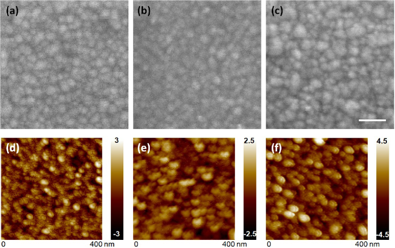
Figure 3. SEM and AFM images of different ZnO-coated Si photocathodes: (a) ZnO(Ar), (b) ZnO(N2) and (c) ZnO:Al. Scale bar in SEM images is 50 nm and the scan range in AFM images was 400 nm.
Download figure:
Standard imageThe I–V behavior of heterojunction photocathodes was tested (figure 4). For comparison, a single-material electrode using Si (figures 2(a)/(d)) alone was studied, which showed limited cathodic current at negative potential and an exponentially increasing anodic current density at positive potentials (figure 4(a) black curve and the inset). Under light illumination, a decrease in the exponentially behaving current density region was noticed under positive potential and a significant photoresponse was noticed in the limited current density region at negative bias. Photo-reduction of water directly at the p-Si electrode surface is slow and inefficient, due to the high overpotential (high kinetic loss) [3], which indicates a large external potential is needed to drive the water reduction reaction. Adding an n/n+ layer on p-Si and formation of the heterojunction photocathode between ZnO and Si improves the interfacial charge transfer kinetics by minimizing electron–hole recombination and assisting in the injection of photogenerated electrons across the ZnO layer to the electrolyte. First of all, with a ZnO coating, the onset potential is effectively reduced, while the current density was enhanced about 20 times at biases above − 1 V (versus Ag/AgCl 1 M KCl) (red curve). Second, ZnO:Al/Si electrodes (dark cyan) showed improved photocurrent level compared to ZnO(Ar) This can be attributed to the conductive nature of the ZnO:Al film (average resistivity 0.1 Ω cm with average carrier concentration of 5.5 × 1019 cm−3, and even as high as 4 × 1020 cm−3 after thermal treatment). The highly doped n-ZnO can potentially increase light absorption due to the larger depletion range in p-Si and also provides a more efficient electron extraction from p-Si as well as transport in ZnO to the electrolyte. Finally, and interestingly, the ZnO(N2) film on p-type Si (50 nm ZnO thickness after 10 min sputtering with a similar deposition rate and under the same sputtering conditions by adding 10% N2 in Ar gas) showed dramatically enhanced photocathodic current, about 80 times at − 1.5 V (versus Ag/AgCl 1 M KCl, blue curve) and a sharper current increase after onset potential, which is even higher than that of Si|ZnO:Al photoelectrodes. The mechanism behind this observation is unclear at this point and further investigation is needed to clarify the enhanced photocurrent effect in ZnO(N2). Note that (i) ZnO films sputtered with and without adding N2 were measured using a four-point Hall measurement, but reasonable readings on resistivity and doping type were not able to be obtained due to the limitation of the Hall measurement set-up, indicating the highly resistive nature of the ZnO film. (ii) Nitrogen's effect on the ZnO impurity energy band shallow/deep or donor/acceptor has been proposed [15–18], which might contribute to the visible light absorption, similar to that in TiO2 [19]. (iii) The ZnO(N2) films showed smaller grain sizes but rougher surfaces, which might lead to a larger effective surface area for catalytic reaction (figures 3(b)/(d)). (iv) ZnO|Si photoelectrodes show large hysteresis in the cathodic I–V scan and waves around − 0.5 V (versus Ag/AgCl 1 M KCl), indicating photochemical instability under PEC operational conditions. Finally, also note in figure 4(a) the anodic photocurrents showed the opposite trend with photocurrent decreasing in the order of ZnO(Ar) > ZnO:Al > ZnO(N2). This trend was fairly consistent with our study on the ITO|ZnO photoanode, where ZnO(Ar) gave the best photoanodic response.

Figure 4. Cyclic voltammetry study of photocathodes with different structure: (a) seeded p-type Si substrate with three different ZnO seeding layers (50 nm). Inset shows planar p-Si photocurrent and dark current. (b) ZnO(N2) seeded p-Si substrate with different seeding layer thickness, under 100 mW cm−2 light illumination. Inset shows the current enhancement factor as the ratio between the net photocurrent from heterostructure (25 nm ZnO(N2) on Si) and bare Si. (c) Dark current of p-Si|ZnO(N2) with different ZnO thickness.
Download figure:
Standard imageThe p-Si photocathode is effectively catalyzed by large bandgap n-type semiconductor material in this case, which can be actually quantified by introducing the definition of the current enhancement factor as the ratio between the net photocurrent from the heterostructure and bare Si (inset of figure 4(b)). Figure 4(b) shows the cathodic photocurrent dependence to oxide film thickness for p-Si|ZnO(N2) samples, where photocurrent at a cathodic bias above − 1 V (versus Ag/AgCl 1 M KCl) decreases with increasing thickness. ZnO has a smaller refractive index than Si over the same wavelength range and thus with ZnO coating it smooths out the refractive index transition from media (aqueous solution) to the Si substrate and minimizes light loss due to reflection. However, a thicker ZnO(N2) film results in a reduced transmittance and increased number of photogenerated holes from ZnO at the ZnO/electrolyte interface (figure 2(b)/(e)), which can significantly degrade the overall cathodic current. Also note that the diminished waves around − 0.5 V (versus Ag/AgCl 1 M KCl) with the increased ZnO(N2) film thickness is presumably due to the improved stability of thicker films. Figure 4(c) shows the dark currents of p-Si|ZnO(N2) with different ZnO thickness. In general and within experimental fluctuation, thicker oxide films produce larger dark current and are more stable.
Figure 5 shows typical SEM images of samples with different lengths of ZnO nanowires from different times of hydrothermal growth (10, 20, 30 min and 2.5 h) on ZnO(Ar) seeded p-Si (figures 5(a)–(d)). The first ever reported ZnO crystal growth based on a hydrothermal method using seed crystals was documented by Laudise in 1960 [20]. Hydrothermal growth of compound materials is a low-cost and low-temperature technique which does not require high-profile equipment. This method has been extensively studied during the last few decades [21–24] and provides an approach to growing micro/nanocrystalline structures on various substrates for flexible and transparent optoelectronics devices. Significant progress on understanding the mechanism to achieve a controllable growth (e.g. crystal size [25], face of growth [26, 27], doping [28] and more) were developed. In our experiment, a thin seeding layer was used providing nucleation sites for nanowire growth, which can differentiate from seedless growth [29]. Preparation of ZnO nanowires on a polished bare Si substrate was done individually from separate processes due to the limited size of the reactor. However, it is confirmed that five samples fabricated separately showed a similar trend within acceptable errors. The cross section of a single ZnO nanowire is a hexagonal wurtzite structure with growth direction along the c axis (figures 5(a)–(d) bottom). As growth time increases, average size and length of ZnO nanowires generally become larger and longer [30], as shown in figure 5(e) (top and bottom). Growth in both length and diameter directions were saturated in the growth versus time curve (figure 5(e)) due to the limited reaction solution (100 ml). Growth rates in the linear fit region (10–30 min) were direction-dependent, with an average growth rate of 28 nm min−1 in the length (axial) direction and about 4 nm min−1 in the diameter (radial) direction. This statistical study showed high yield of device fabrication and repeatability from substrate cleaning, seeding layer sputtering and nanowire syntheses.
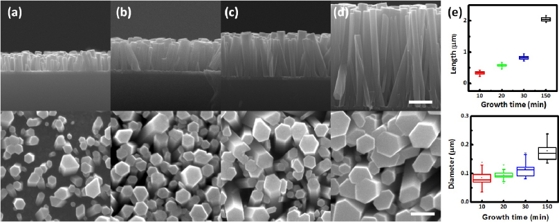
Figure 5. SEM images of ZnO nanowires on polished p-type Si from different growth times of (a) 10 min, (b) 20 min, (c) 30 min and (d) 2.5 h. First row (top): cross-sectional view (scale bar = 500 nm) and second row (bottom): top view (scale bar = 200 nm). Seeding layer here is 60 nm ZnO(Ar). (e) Statistics of nanowire length (top) and diameter (bottom) with sampling size of 20.
Download figure:
Standard imageFigure 6 shows the I–V characteristics of the photocathodes of ZnO nanowires with different growth times on 50 nm ZnO(N2) seeding layer on p-Si. All the data reported here were measured from at least three samples. With the increasing nanowire growth time, photocurrent density and catalytic effect initially increase from 0 min (seeding layer only, black curve) to 10 min (red curve) and 20 min (blue curve) growth, and decrease with growth time for longer nanowires, e.g. 30 and 60 min growth (dark cyan and magenta curves in figure 6, respectively). The peak photocurrent densities were summarized in figure 6, inset, with a peak photocurrent of 4.2 mA cm−2 for 20 min growth of ZnO nanowires at − 1.5 V (versus Ag/AgCl 1 M KCl). These data suggest that the dependence of photocurrent to nanowire growth time is an overall effect of surface area (increase with nanowire length and thus growth time), ratio of accessible effective surface area (decrease with nanowire radius and thus growth time), light absorption (increase with nanowire length and thus growth time), charge separation and transport efficiency (decrease with nanowire length and thus growth time), surface trap states (decrease with nanowire radius and thus growth time), etc. Cathodic waves around − 0.5 V (versus Ag/AgCl 1 M KCl) also showed length-dependent behavior, where longer nanowires showed minimum cathodic wave. This is believed to be due to the longer growth time which leads to an increase in nanowire array density and results in a reduced overall exposed area to the electrolyte.
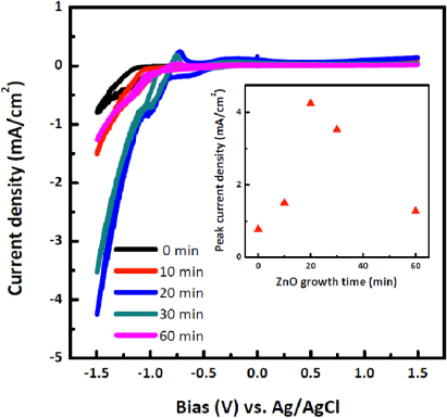
Figure 6. Cyclic voltammetry on p-Si|ZnO(N2, 50 nm)|ZnO nanowire with various nanowire growth times.
Download figure:
Standard imageThe hydrogen evolution reaction (HER) catalyst remains an important part of the hydrogen economy for the conversion processes of H+ to H2 in artificial photosynthesis, as well as the reverse reaction of H2 to H+ in fuel cells. Platinum is the well-accepted and most-efficient HER catalyst. However, Pt metal is not able to meet large-scale production applications due to its limited availability and high cost. In order to address this problem, researchers are actively seeking non-noble alternatives. These alternatives containing metals from the transition metals in the form of heterogeneous metal alloy (Mo–Ni [31], Al–Ti [32]), metal oxides/sulfides (MoSx [33]) or enzyme hydrogenases-like complexes (Pt-complex [34], Ni–Ru complex [35], Co-complex [36]) are the three major categories of catalysts attracting research interest. In this work, Ni, Pt and Pd metal were deposited on ZnO thin-film-coated p-Si, as well as ZnO nanowire-coated p-Si in order to reduce the overpotential. 5 nm of metal was coated on ZnO using e-beam evaporation. This thickness was chosen to produce a non-continuous film to minimize the loss of incident light. Compared to Pt, Ni and Pd showed higher activity on sputtered ZnO(N2) film, as shown in figure 7(a). Direct metal coating on planar p-Si showed electrocatalysis in dark and minimized the photoresponse under cathodic bias. Metal catalyst deposited on the semiconductor surface dramatically decreases the photovoltage since it effectively lowers the energy barrier at the semiconductor/electrolyte interface, resulting in an enhancement in carrier recombination [10]. Using ZnO as an intermediate layer helps to maintain the photovoltage at ZnO/Si junction, which effectively separates the photogenerated carriers from Si and enhance the transport in ZnO and to the ZnO/electrolyte interface.
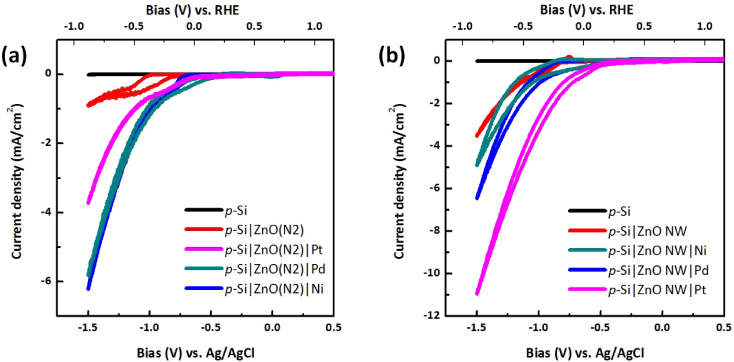
Figure 7. Cyclic voltammetry (CV) graphs of various metal co-catalyst-coated Si substrates without ZnO nanowires (a) and with ZnO nanowires (b). Seeding layer used was ZnO(N2, 50 nm).
Download figure:
Standard imageFigure 7(b) shows the photoelectrochemical activity increase of samples with metal coatings on ZnO nanowires in the order of Ni < Pd < Pt. The reason for this difference in catalytic activity of metals on ZnO thin film versus those on nanowires is not clear. One possibility is the difference in light scattering/absorption from the metal coating: light scattering from the metal coating on ZnO nanowires is minimal due to the vertical nanowire geometry and the light trapping effect. Pt showed higher activity on nanowire samples than on thin films, presumably due to improved catalytic behavior from the rough metal coating on nanowires. Moreover, it has been pointed out that electroless-deposited metals showed better performance than gas-phase-deposited metal film in terms of the catalytic effect due to the smaller particle sizes and larger surface area. However, we were not able to apply the metal nanoparticles to ZnO by electrochemical methods due to its fairly weak chemical stability in various pH environments. The bias scale versus Ag/AgCl 1 M KCl is converted to reversible hydrogen electrode values (top x axis in figure 7), which is independent of pH can be converted using the equation [37]

where  is the potential difference to the standard hydrogen potential, which is 0.236 V. One can see that metal coating effectively moves the onset potential, defined as when the photocurrent density exceeds 0.1 mA cm−2, below the zero RHE level.
As mentioned earlier, the hysteresis of I–V scan indicated chemical instability of the photoelectrodes. Actually, ZnO is an amphoteric metal oxide which reacts with both acids and bases. An acidic environment has a much faster etching rate than a basic solution. Under bias, ZnO cathodic decomposition in acidic conditions and photodecomposition of ZnO is normally a concern when used as a photoanode.
Cathodic decomposition [38]:

Photoanodic decomposition [39]:

To better understand the photoelectrochemical stability of Si|ZnO photocathodes, samples after a typical I–V scan in dark and under illumination in an electrolyte with pH of 7.2 were investigated under SEM. As shown in figure 8, oxide particles (via SEM-EDX) were noticed on both ZnO thin-film and nanowire-coated p-Si after I–V scans. Figures 8(a) and (b) show the cross-sectional images of the ZnO thin films and changing into oxide particles, while figure 8(c) shows the top view of the re-deposited oxide particles. Figures 8(d)–(f) show the cross-sectional images of a p-Si|ZnO nanowire photoelectrode in pristine condition, after one typical I–V scan, and tested under illumination and biased at − 1.5 V (versus Ag/AgCl 1 M KCl) for 1 h, respectively. Even more severe damage of ZnO and even complete removal was noticed in acidic and basic solutions. Metal co-catalyzed photoelectrodes showed improved stability and minimized the cathodic decomposition, in addition to the strong effect of improving the electrochemical hydrogen reduction kinetics. For example, figure 8(h), compared to (g), shows platinum-metal-coated p-Si|ZnO nanowires with minimized damage after I–V scans, which is also shown by the cross-sectional SEM of photoelectrodes tested under illumination and biased at − 1.5 V (versus Ag/AgCl 1 M KCl) for 1 h in figure 8(i) compared to figure 8(f).

Figure 8. SEM images of photoelectrochemical stability: (a) cross-sectional view of p-Si|ZnO(N2, 50 nm) photoelectrode at pristine condition, (b) cross-sectional view and (c) top view after one typical dark/photo I–V scan; cross-sectional view of p-Si|ZnO(N2, 50 nm)|ZnO NW(20 min) photoelectrode at (d) pristine condition, (e) after one typical dark/photo CV scan and (f) tested under illumination and biased at − 1.5 V (versus Ag/AgCl 1 M KCl) for 1 h; 45° view of p-Si|ZnO(Ar)|ZnO NW (30 min)|Pt photoelectrode at (g) pristine condition, (h) 45° view and (i) cross-sectional view of the tested sample under illumination and biased at − 1.5 V (versus Ag/AgCl 1 M KCl) for 1 h.
Download figure:
Standard image4. Conclusions
We report the systematic study of Si|ZnO and Si|ZnO| metal photocathodes for effective photoelectrochemical cells and hydrogen generation, where ZnO was in the form of nanocrystalline thin films and vertical nanowire arrays. ZnO thin films were deposited on p-Si under Ar or Ar/N2 mixture atmosphere and 2% Al2O3-doped ZnO thin films were studied. ZnO coatings increase the photocathodic current due to the formation of a p/n junction, thus improving charge separation. The doped ZnO:Al (n+-ZnO) thin films further increase the cathodic photocurrent because of higher conductivity. Interestingly ZnO thin films prepared in N2/Ar gas demonstrated the highest enhancement in photocurrent, which is probably due to increased light absorption in the visible range (due to N levels in ZnO) and to increased surface area due to smaller nanocrystal sizes. An optimal oxide thickness of around 25 nm was found for the best photocurrent enhancement. Growth of vertical ZnO nanowires, with optimal growth time on Si|ZnO was found to dramatically increase the photoelectrochemical efficiency due to the enhanced light absorption and enlarged surface area. Metal co-catalysts on ZnO to further catalyze the hydrogen evolution reaction were studied and Ni was demonstrated to have comparable catalytic activities to that of expensive Pt and Pd. Finally, the photoelectrochemical instability of Si|ZnO photoelectrodes was demonstrated in pH neutral electrolytes, which can be minimized by metal co-catalysts. Co-catalysts using metal and metal oxides on p-type Si provide a low-cost and scalable solution for improved performance of photocathodes for practical applications in clean solar energy harvesting and conversion to clean H2 fuel.
Acknowledgments
DW would like to thank the Department of Energy (DOE DE-FG36-08G018016) and the National Science Foundation (NSF ARRA ECCS0901113) for financial support. KS would like to thank Professor S Jin for stimulating discussion. KM would like to thank the UCSD Cal-IT2 undergraduate student summer research program. WB would like to thank the UCSD international summer program. The authors would like to thank W Chen and Professor P Yu for help in Hall measurement.