
Abstract
We simultaneously measured the force and tunneling current in three-dimensional (3D) space on the Si(111)-(7 × 7) surface using scanning force/tunneling microscopy at room temperature. The observables, the frequency shift and the time-averaged tunneling current were converted to the physical quantities of interest, i.e. the interaction force and the instantaneous tunneling current. Using the same tip, the local density of states (LDOS) was mapped on the same surface area at constant height by measuring the time-averaged tunneling current as a function of the bias voltage at every lateral position. LDOS images at negative sample voltages indicate that the tip apex is covered with Si atoms, which is consistent with the Si–Si covalent bonding mechanism for AFM imaging. A measurement technique for 3D force/current mapping and LDOS imaging on the equivalent surface area using the same tip was thus demonstrated.
Export citation and abstract BibTeX RIS
For more information on this article, see LabTalk.
1. Introduction
Atomic force microscopy (AFM) as well as scanning tunneling microscopy (STM) allow for the imaging of individual atoms on various surfaces and for the measurement of a variety of local physical quantities [1, 2]. The frequency modulation technique [3] is usually used for AFM imaging with atomic resolution in an ultra-high vacuum. In this method, the main observable quantity is the frequency shift (Δf) of an oscillated cantilever caused by the interaction force between the tip apex atoms and surface atoms (F). The interaction force with the tip at specific sites on the surface can be quantified by the tip–surface distance dependence of the Δf data [Δf(z)], which is termed force spectroscopy. Since the landmark demonstration of the detection of a single chemical bond between a tip apex Si atom and an Si atom on the Si(111)-(7 × 7) surface [4], the capability of site-specific force spectroscopy has been demonstrated, including chemical identification through the maximum attractive chemical bonding force on semiconductors [5], quantification of the force related to mechanical atom manipulation [6–9], and direct measurement of magnetic exchange interaction [10]. Point force spectroscopy has been developed into a 2D/3D force mapping technique, where Δf data are acquired in the plane/volume on surfaces and converted to an F map. Various force mapping results have been reported on metal surfaces [7, 11], semiconductor surfaces [12, 13], insulator surfaces [14–19], and molecules [20–25]. AFM, which was previously a surface imaging tool through the indirect quantity Δf, is now a direct visualization tool of the force field on surfaces.
STM is generally used to measure the tunneling current (It) between the tip and a sample. Crucially, using STM, we can access an important quantity, the local density of state (LDOS), on surfaces by scanning tunneling spectroscopy (STS), where the tip–sample bias voltage (Vs) dependence of It [It(Vs)] is measured [1, 26]. Current imaging tunneling spectroscopy (CITS) is a well established technique to visualize the LDOS with high resolution [27]. dIt/dVs is mapped by a lock-in technique or numerical calculation of the It(Vs) spectra at each lateral point during an STM topographic scan. This method has been used for various purposes, such as chemical identification [28] and investigation of the local electronic state on nanostructures created by manipulation of atoms [29–31].
Using conductive tips and samples, combined AFM/STM measurements on the same surface area become possible. Since AFM and STM yield complementary quantities, combined measurements offer a powerful method to investigate mechanical and electronic properties on surfaces with atomic scale resolution. In particular, simultaneous AFM/STM operation is preferred since we can check whether the tip apex atom for AFM is coincident with that for STM [32]. Constant height scanning is important for reliable simultaneous AFM/STM imaging without crosstalk through the topographic effect [7, 32–35]. A few combined AFM/STM spectroscopic experiments have been demonstrated, such as multiple measurements of the work function [36], comparison of the imaging distance between AFM and STM [32], investigation of the current drop phenomenon due to chemical bonds [35, 37, 38], and investigation of the fundamental relation between force and tunneling current [39–41]. Point force spectroscopy and STS measurements above the same atom with the same tip have been demonstrated [35]. Nevertheless, combined 3D force mapping and CITS measurements, i.e. force field imaging and LDOS imaging on the same surface area, offer great promise to visualize the spatial distribution of the localized electronic states associated with force and the electronic states located near the Fermi level on various surfaces and nanostructures.
In this paper we present a method for 3D force/current mapping and CITS measurements on the same surface area with the same tip at room temperature to yield a complete combined AFM/STM spectroscopic technique. The main difficulty in such a mapping technique is thermal drift of the tip position relative to the surface during time-consuming data acquisition. In particular, a drift in the tip–surface distance during mapping disrupts the data, and in the worst case scenario causes a tip–surface crash. In the past, 3D force mapping has been carried out under cryogenic temperatures where the thermal drift is negligibly small and/or using a drift compensation mechanism at specified time intervals during mapping. In the present study, the long-range force was used to maintain the tip–surface distance during mapping acquisition [10]. This also allowed us to obtain CITS data at a constant height, which can remove topographic artifacts in traditional LDOS images using STM.
The remainder of the present paper is organized as follows. The conversion formulae between observables in AFM/STM and physical quantities of interest are described in section 2. We present the experimental method used in section 3. Results and discussion are presented in section 4. Finally, our concluding remarks are presented in section 5.
2. Conversion formulae
In the operation of dynamic AFM/STM, the observables depend on measurement parameters and are not the direct physical quantities of interest. Here, we describe formulae for the conversion to parameter-independent physical quantities. In dynamic STM, the tunneling current flows instantaneously at a close tip–surface distance during cantilever oscillation. A time-averaged tunneling current (〈It〉) is then detected since the bandwidth of the current-to-voltage converter is usually much smaller than the resonance frequency of the cantilever. On the other hand, Δf results from the mechanical response of the cantilever to F. 〈It〉 and Δf are thus the observables in AFM/STM. In view of cantilever dynamics, the relation between the observables and physical quantities of interest, i.e. F and instantaneous It, can be written as follows:

and

where f0, k, A, and z are the resonance frequency, the spring constant, the oscillation amplitude of the cantilever, and the distance of closest approach between the tip and sample, respectively [42–46]. Δf (〈It〉) is calculated by the weighted average of F (It) over the tip oscillation from the closest point to the surface (u =− 1) to the farthest point from the surface (u = 1).
In equations (1) and (2), Δf(z) and 〈It(z)〉 are expressed as a function of F(z) and It(z), respectively. To convert the observables in distance spectroscopy, i.e. Δf(z) and 〈It(z)〉, into F(z) and It(z), these formulae need to be inversely solved. Since there are no exact solutions, methods for solving these inverted problems have been proposed. In figure 1, practical and useful analytical formulae for AFM (upper) and dynamic STM (lower) are summarized in the form of a flow chart. If the observed Δf(z) [〈It(z)〉] has exponential distance dependence as a special case, equation (1) (equation (2)) can be analytically solved and simple solutions using the Kummer function are obtained as equation (3) (equation (7)) [45]. It can then be seen that F(z) [It(z)] also has exponential distance dependence. The exponential distance dependence of F(z), however, is not probable in reality, except for the chemical bonding force that can be ideally described by a Morse type force. F(z) is usually very different from a simple exponential and is not even monotonic due to the transition from an attractive to a repulsive force. On the other hand, exponential distance dependence of It(z) is probable, as is well known in STM [1]. Nevertheless, at close tip–surface distances, where the atomic force is significant, It(z) deviates from the exponential dependence due to relaxation of the tip and surface atoms [41] and LDOS modification [37]. In general, equations (3) and (7) and the corresponding large amplitude formulae (equations (4) and (8)) do not hold.
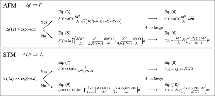
Figure 1. A summary of useful analytical conversion formulae from Δf to F (upper panel) and from 〈It〉 to It (lower panel) in flow chart form. If Δf(z) [〈It(z)〉] has an exponential distance dependence, F(z) [It(z)] can be simply described using the Kummer function,  , as equation (3) (equation (7)). In general, we cannot expect such a simple form for Δf(z) and 〈It〉 at close tip–surface distances. In such cases, an approximation formula with high accuracy, equations (5) and (9), is available, which holds for any distance law. Equations (3), (5), (7), and (9) that hold at any cantilever oscillation amplitude can be simplified as equations (4), (6), (8), and (10) at large amplitudes.
Download figure:
Standard imageFor practical simultaneous AFM/STM spectroscopy, the inversion formulae that hold for general distance dependence are necessary. Fortunately, an approximate formula with high accuracy has been implemented for both Δf [47] and 〈It〉 [48], as shown by equations (5) and (9), respectively. These formulae include integration that requires numerical calculation, but they are still useful. In both equations (5) and (9), the first term corresponds to a small cantilever oscillation amplitude solution, the second term is the large amplitude solution, and the third term offers a correction for the intermediate amplitude. The second terms are exactly the same as the large amplitude formulae analytically derived by Durig [43, 44]. These are written as equations (6) and (10) in figure 1. Here, a large amplitude means that the cantilever oscillation amplitude is so large that F (It) becomes zero at the farthest point of the tip from the surface during the cantilever swing. It is to be noted that the required values of A are different in equations (6) and (10). Equation (10) holds even at much smaller A than for equation (6), because It only has a short-range origin whereas F includes a long-range part, such as the van der Waals force and the electrostatic force.
3. Experimental details
3D force/tunneling spectroscopic measurements were carried out using a custom-built room temperature AFM/STM. Commercial PtIr-coated Si cantilevers (NCLPt, NanoWorld AG, Switzerland) were cleaned by Ar ion sputtering prior to use. The sputtering conditions used are crucial for high conductivity of the tip for STM and sharpness of the tip apex for AFM. The cantilever, the deflection of which was detected by a home-built optical interferometer, was oscillated with constant amplitude by a commercial AFM controller (easy PLL plus, Nanosurf, Liestal, Switzerland). AFM/STM imaging and 3D force/tunneling spectroscopy were carried out using a commercial scan controller (Dulcinea, Nanotec, S.L., Madrid, Spain) [49]. We used Sb-doped Si(111) substrates as samples, which had a resistivity of 0.01 Ω cm. The Si(111)-(7 × 7) reconstructed surfaces were prepared by the standard method of flashing and annealing the samples. 〈It〉 was detected from the tip by a home-built current-to-voltage converter, while Vs was applied to the sample with respect to the tip that was virtually grounded. Since the AFM channel is optically detected, the AFM signal could be safely separated from the STM channel.
In this study, Δf and 〈It〉 were simultaneously measured in 3D space on the Si(111)-(7 × 7) surface at room temperature. The Δf(x,y,z) and 〈It(x,y,z)〉 data were acquired with 64 pixels × 64 pixels × 256 pixels. Successive distance spectroscopy, i.e. measurement of Δf(z) and 〈It(z)〉, was carried out at each pixel in the grid. One 3D mapping datum required about 500 s. A key idea for reliable measurement with reasonable acquisition time is the use of site-independent long-range interaction force to adjust the tip–surface distance at each pixel before the distance dependence is measured. The tip approaches the sample from the Δf-constant surface with AFM feedback, which is almost flat in the long-range force region. The tip–surface distance fluctuation in the maps is less than 10 pm, which was estimated by the AFM topographic image that was simultaneously obtained. We used the feedforward technique to compensate for the lateral thermal drift [12]. Using the same tip at the same location, the Vs dependence of Δf and 〈It〉 was subsequently measured in the plane parallel to the surface while AFM feedback was again used. The Δf(Vs) and 〈It(Vs)〉 data were acquired at Vs =− 2–2 V with 44 points on each pixel of 64 × 64. This required about 570 s. The present CITS measurements at a constant height mode could remove topographic crosstalk. In traditional CITS, the It(Vs) curve is recorded at each pixel in the STM topography, where the tip height is strongly affected by the electronic states corresponding to the Vs used [50].
The experimental procedure used is as follows. The tip is scanned on the surface by AFM topographic feedback. Vs is fixed to the value of the contact potential difference (VCPD) to minimize the long-range capacitive electrostatic force. The location to be investigated by the 3D force/tunneling spectroscopy is chosen at the center of a terrace. The tip–surface distance is adjusted to the position in the long-range force region, where no atomic contrast appears in either AFM or STM, by changing the Δf setpoint for feedback. 3D force mapping acquisition then starts. The tip–surface distance is stabilized by Δf, z feedback is temporarily opened, and the tip approaches the surface from the feedback distance with Δf(z) and 〈It(z)〉 being recorded. After the tip is retracted back to the original height, the distance feedback is reactivated to adjust the tip–surface distance. The tip is laterally moved to the next point in the x–y grid with AFM feedback and the acquisition of Δf(z) and 〈It(z)〉 are repeated at each pixel. After 3D force/current mapping acquisition, the tip–surface distance is adjusted to the height for CITS measurement where atomic contrast appears in STM, but the site-independent long-range force is still dominant (poor atomic contrast in AFM). We can find this distance because the optimal tip–surface distance for imaging is different between AFM and STM [32]. CITS measurement is then carried out. After the tip–surface distance is stabilized, the AFM feedback is temporarily opened, and Vs is swept recording Δf and 〈It〉. Then, the feedback is reactivated to adjust the distance and the tip moves to the next grid. The acquisition of Δf(Vs) and 〈It(Vs)〉 data is repeated until the tip visits all the pre-determined grid points. The LDOS spectra were obtained by differentiating the 〈It(Vs)〉 curves numerically.
4. Results and discussion
One of our data sets of simultaneous 3D force/current mapping is shown in figure 2(a) for Δf(x,y,z) and (b) for 〈It(x,y,z)〉. We defined the origin of the tip–surface distance (z = 0) as being the z such that the conductivity (G = It/VS) extrapolated from the exponential distance dependence of G at far distances becomes 2e2/h = (12 906 Ω)−1. The top sides of the 3D maps correspond to the farthest plane from the surface in data acquisition, where the long-range force is dominant and atomic contrast does not appear in the Δf image as well as 〈It〉. At closer distances, the site-specific force offers atomic resolution in Δf. 〈It〉 also shows atomic contrast in the tunneling regime. The images cut from these maps in the x–y plane well reproduce our simultaneous AFM/STM images at constant height [32]. The atomic contrasts are clearly different between Δf and 〈It〉, reflecting the different imaging mechanisms. In the present study, 256 frames of constant height images with different tip–surface distances were acquired. These dense data in the z direction allow for conversion of the observed maps to the physical quantities of interest.
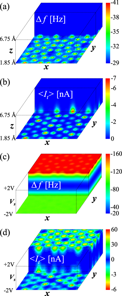
Figure 2. 3D force/current maps and bias spectroscopic data using the same tip. The 3D maps, for (a) Δf(x,y,z) and (b) 〈It(x,y,z)〉, were acquired in the volume of 5.16 nm × 5.16 nm × 0.49 nm with 64 pixels × 64 pixels × 256 pixels at Vs = VCPD =− 300 mV. (c) Bias force spectroscopy [Δf(x,y,Vs)] and (d) CITS [〈It(x,y,Vs)〉] were performed at Vs =− 2–2 V with 44 points on the same surface area as (a) and (b) at constant height corresponding to z = 3.37 Å. The other acquisition parameters are f0 = 151 969 Hz, k = 23.0 N m−1, A = 150 Å, respectively.
Download figure:
Standard imageThe Δf and 〈It〉 maps were converted to the short-range force map [FSR(x,y,z)] and It(x,y,z). To estimate the long-range force contribution in Δf, a Δf(z) curve above the corner hole is fitted into the inverse-power function of z−s. For the best fit, s = 1.09 was obtained, which corresponds to z−1.59 of the distance dependence of the long-range force [45]. The short-range Δf (ΔfSR) map was then obtained by subtraction of the fitting curve from each Δf(z) curve at every lateral point. The ΔfSR map was converted into the FSR map using the inversion formula (equation (5)). Since there is no atomic contrast in the simultaneously obtained dissipation channel, the potential energy and the lateral force can also be calculated (not shown) [12, 13, 51]. The 〈It〉 map was directly converted into the It map using the formula in equation (9). FSR and It images cut from the maps in the x–y plane are shown in figure 3. The tip–surface distance in figures 3(a) and (b) corresponds to the bottom plane in figures 2(a) and (b). Both FSR and It show clear atomic contrast. Since the atom positions in AFM perfectly coincide with those in STM, the same tip apex atom contributes to both chemical bond and current [32]. AFM detects the attractive force pulling the tip down toward adatom sites, while in STM, the tunneling electrons from the adatoms to the tip apex atom are detected (Vs =− 300 mV). Note that if AFM and STM data are sequentially acquired instead of simultaneous measurement, it is hard to confirm whether an atom on the tip apex as the force probe coincides with an atom as the current probe [32].

Figure 3. FSR and It images cut from the corresponding 3D maps converted from figures 2(a) and (b): (a), (b) z = 1.85 Å and (c), (d) z = 4.30 Å. (e) FSR(z) and It(z) curves above the corner adatom in the faulted half unit cell marked by the symbols in the images.
Download figure:
Standard imageImportantly, It on the adatom sites in figure 3(b) is huge; a few hundred nA was obtained in the chemical bonding regime. On the other hand, in figures 3(c) and (d), obtained at the retracted distance from the bottom of 2.45 Å, FSR does not show atomic contrast while the value of It is a few nA, similar to the typical values in conventional STM. These results reproduce our previous conclusion that the traditional STM imaging distance is larger than the chemical bonding distance by a few Å [32].
This is also clearly seen in the distance curves. FSR(z) and It(z) curves above the corner adatom in the faulted half unit cell are shown in figure 3(e); these were extracted from another map obtained by the same tip. FSR(z) becomes more attractive with decreasing tip–surface distance and reaches a maximum attractive force of −1.5 nN. The tendency of the FSR(z) curve is the same as that of previous force curves obtained on the same surface [4, 6, 13, 52–54]. At z > 3 Å, It exponentially increases with decreasing tip–surface distance with a decay constant of κ = 20.1 ± 0.2 nm−1, where I(z) ∝ exp(−κz). It reaches 43 nA at z = 3 Å. At z < 3 Å, the distance dependence deviates from the exponential, with a peak of 340 nA around z = 1.45 Å. This current drop around the chemical bonding regime was found by static STM [37] and reproduced by our simultaneous force/tunneling spectroscopy [35, 38]. This remarkable phenomenon was explained as LDOS modification by chemical bond formation between the tip and surface atoms [37].
Vs was fixed at VCPD during the 3D mapping described above, while the Vs dependence of It provides the energy for the specific surface states. Figure 2(d) shows the CITS data, i.e. 〈It(x,y,Vs)〉, obtained on the same surface area with the same tip as the 3D maps. The top side in the 〈It(x,y,Vs)〉 map is the 〈It〉 image at Vs = 2 V while the bottom plane corresponds to Vs =− 2 V. The tip–surface distance was maintained at z = 3.37 Å where the effect of the chemical bonding force on LDOS is negligible [37]. 〈It〉 images are clearly different between Vs = 2 V and Vs =− 2 V, reflecting empty and filled electronic states, respectively. The rest atoms are resolved in the filled states. Using CITS measurements, the 〈It(Vs)〉 curve can be derived at any specific site on the surface. Figure 4(e) shows the LDOS curves above the corner adatom and the rest atom in the faulted half unit cell marked in the images. Since the 〈It(z)〉 curves have exponential distance dependence at z > 3 Å, the normalized conductance [(dIt/dVs)/(It/Vs)] can be calculated from the 〈It(Vs)〉 curves; the coefficients of the Kummer function in the numerator and denominator of the normalized conductance cancel each other (see equation (7)). Our LDOS spectra are in good agreement with previous STS results [26, 55, 56]. In the filled state, the peak is observed around −330 mV on the adatom, while a prominent peak on the rest atom state is clearly observed around −700 mV. In the empty state, at the edge of the conduction band, a shoulder is observed around 400 mV, which corresponds to an adatom state.
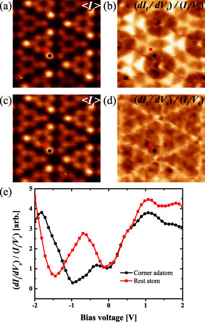
Figure 4. 〈It〉 and LDOS images at (a), (b) Vs =− 700 mV and (c), (d) Vs =− 1350 mV. The images are obtained from figure 2(d). (e) LDOS curves above the corner adatom and the rest atom in the faulted half unit cell marked by the symbols in the images.
Download figure:
Standard imageThe CITS measurement produces the spatial distribution of LDOS at a specific energy. In figure 4, 〈It〉 and (dIt/dVs)/(It/Vs) images at (a), (b) Vs =− 700 mV and (c), (d) Vs =− 1350 mV are shown. The 〈It〉 images are similar for Vs =− 700 and −1350 mV. In contrast, LDOS images are clearly different. At Vs =− 700 mV, the triangle feature appear at rest atom sites in the LDOS image, consistent with previous CITS measurements [27, 56–58]. At Vs =− 1350 mV, the LDOS image shows a different pattern. In the negative Vs, electrons tunnel from the sample with the energy mainly near the Fermi level to the tip [1]. Therefore, the contribution of the electronic structure of the sample to LDOS contrast is relatively small. The observed variety in the LDOS contrast at negative Vs indicates that the DOS of the tip is not flat but has an energy structure [57]. We usually change the tip apex state by an intentional controlled tip crash to the surface until atomic contrasts are obtained in both AFM and STM. It is probable that the tip apex is covered with Si atoms extracted from the Si surface. Actually, the LDOS contrasts in both figures 4(b) and (d) are in good agreement with the pattern obtained by theoretical calculation using the Si tip model [57, 59]. They also simulate the LDOS image using the W tip model, by which the LDOS contrast does not depend on Vs very well at negative polarity due to the structureless DOS as the metallic character of the tip. Our conclusion that the tip apex is covered with Si atoms is also consistent with the Si–Si covalent bonding model proposed as an AFM imaging mechanism [60].
During CITS measurement, Δf(x,y,Vs) was simultaneously recorded as shown in figure 2(c). The local contact potential difference (LCPD) can be derived from Vs for the minimum of the parabolic Δf(Vs) curve [61]. In the observed Δf(x,y,Vs), LCPD does not show atomic contrast since the tip–surface distance is not small enough to induce charge polarization on the surface [62].
The Vs dependence of Δf is parabolic at small Vs, whereas it deviates from the parabola in the large Vs region, where 〈It〉 becomes prominent. Δf images at large Vs show atomic contrast, as shown in figure 2(c), although the tip–surface distance is in the region dominated by long-range force. This contrast is formed by suppression of |Δf| on the sites where 〈It〉 is huge. Therefore, the contrast pattern in Δf looks the same as in 〈It〉. This phenomenon has been reported recently on the Si(111)-(7 × 7) surface using a self-detection type of AFM/STM [63]. They attributed this |Δf| reduction by the tunneling current to the suppression of Vs due to the finite electrical resistivity of the charge accumulation area below the tip. This Vs reduction in turn lowers the electrostatic force, which results in apparent atomic resolution in AFM. This phenomenon may affect our STS spectra at large Vs. In our study, however, since the cantilever oscillation amplitude is large, a comparison with the proposed model is not straightforward. Further experiments will be performed in future work.
5. Summary
We have demonstrated simultaneous force/current mapping in 3D space and CITS measurements on the same area of a Si(111)-(7 × 7) surface using the same tip state. In the proposed method, reliable data sets can be obtained even at room temperature. This combined experiment allows for the investigation of mechanical properties of the force field and electronic properties of LDOS on the same target. Using this method, we can evaluate the properties of self-assembled nanostructures or artificial nanostructures created by atomic manipulation [64]. In addition, the interaction force and LDOS can also provide useful information to identify the tip apex structure and composition with help from theoretical calculations.
Acknowledgments
This work was supported by a Grant-in-Aid for Scientific Research (22221006, 19053006, 21246010, 21656013, and 22760028) from the Ministry of Education, Culture, Sports, Science and Technology of Japan (MEXT), the Funding Program for Next Generation World-Leading Researchers, the Japan Science and Technology Agency (JST), Handai FRC, the project Atomic Technology funded by MEXT, and Global COE programs.