

Abstract
We investigated the transport properties of a curved iron-based superconducting whisker, a geometry which is considered to be interesting for electronic applications. The current–voltage characteristics (IVCs) are bi-stable at low temperatures, exhibit multiple branches at intermediate temperatures and are continuous but nonlinear at temperatures close to the superconducting transition temperature Tc. Low temperature scanning laser microscopy revealed that the multiple branches arise from a localized hot spot which for the different branches appears at different positions along the whisker. By contrast, at low temperatures Joule heating completely overheats the sample to temperatures above Tc in the resistive state. Close to Tc, the hot spot disappears and the IVCs are continuous. In the multiple-branch region, the whisker can be switched between different states by laser irradiation, provided that the laser is positioned at the location of the hot spot. The effect could be interesting for using the whisker as a photon detector or as a position-sensitive opto-electronic switch.
Export citation and abstract BibTeX RIS
1. Introduction
High critical temperature (high- ) cuprate superconducting whiskers, having cross sections of only a few μm but a length on the millimeter scale, have attracted a lot of interest both for fundamental research and potential applications in electronic devices [1]. Typically, the whiskers are straight along their long side. An interesting variant is whiskers that are highly curved. Such whiskers may be interesting for electronic devices as well [2, 3]. The curved whiskers contain defects, and Josephson junctions or phase-slip centers might naturally appear in these objects. However, the existing reports on curved cuprate superconducting whiskers either focused on the growth mechanism [2], or on the detection of defects by nanoprobe and single-crystal x-ray diffraction techniques [3]. To our knowledge there is no report about the electrical transport properties, which is essential for electronic devices.
Thus, it is not only interesting to extend such investigations to other materials but is also necessary to study these curved objects with respect to electrical transport. In this article, we report results obtained on a curved Ba1−xKxFe2As2 superconducting whisker, with a Tc of about 25 K. The whisker was investigated via transport measurements and low temperature scanning laser microscopy (LTSLM), a technique which has been used to study a lot of different superconducting devices, including high-Tc superconducting terahertz emitters, or superconducting resonators [4–8]. In a certain temperature range, several voltage jumps and resistive branches were found in the current–voltage characteristics (IVCs). Such branches may result from the Josephson effect [9, 10], phase-slip centers [11, 12], from vortex instabilities [13–15] or from localized hot spots, i.e. regions heated to temperatures above Tc [16]. LTSLM revealed that on each resistive branch on the IVCs, a localized hot spot exists. The position of the hot spot is different for each branch. No indications of, e.g. a Josephson-junction-like behavior or of phase-slip physics were found. Under certain conditions, the hot spot revealed to be very sensitive to external perturbations, e.g. laser irradiation in our experiment. As a result of the perturbation, the IVC switches from one branch to another. With this feature, curved whiskers have the potential to be used as a photon detector or as a position-sensitive opto-electronic switch.
2. Experimental methods
The whisker introduced here was found to grow randomly on Ba1−xKxFe2As2 tape which was initially prepared for high power application [17, 18]. The basic preparation for the Ba1−xKxFe2As2 tape is: the precursors are prepared from Ba filings (99%), K plates (99.5%), Fe powder (99.9%) and As pieces (99.99%). They are ground into powder in an agate mortar in a glove box filled with high-purity Ar gas, and then pressed into pellets. The pellets are heat treated at 1100 °C for 0.5–2 h, then gradually cooled to 900 °C and finally cooled in the furnace down to room temperature. Whiskers then grow randomly on the surface of the pellets as shown by the scanning electron microscope image in figure 1(a). The doping concentration x of the pellets, as determined by energy dispersive x-ray spectroscopy (EDX), is around 0.34–0.43. The EDX of narrow whiskers show a similar ratio in composition. However, the EDX of a wide whisker shows an atomic ratio of Ba:K:Fe:As to be around 0.09:0.04:0.63:0.24. Although these whiskers have different shape, they all show curved features.

Figure 1. (a) SEM image showing whiskers with curved features formed randomly on the surface of Ba1−xKxFe2As2 pellets. (b) Resistance R versus bath temperature Tb, measured with a bias current of about 80 μA. The midpoint of the superconducting transition is 24 K, and the transition width is 2 K. The profile of the whisker and the terminal configuration are shown in the inset. The width of the whisker is about 5 μm. Several bends can be seen. Between the two voltage electrodes there is a bend with an angle of about 26°.
Download figure:
Standard image High-resolution imageBeyond the interesting growth mechanism causing the curved features, these whiskers could have some potential for electronic devices. This triggered our study of transport properties presented in this paper. To perform electric transport measurements, we pick up a whisker with several bends and glue it to an MgO substrate with epoxy resin. The smoothly varying width of the whisker presented in this study is about 5 μm. Its thickness is about 300 nm. After gluing, an Au layer with a thickness of about 30 nm is thermally evaporated. Four electrodes are patterned on the whisker by photolithography and wet etching, as shown in the inset of figure 1(b). Between the two voltage electrodes the whisker has a bend with an angle of about 26°, see dashed white box in figure 1(b).
To perform cryogenic measurements, the sample is mounted on a copper plate cooled by liquid helium in a home-made system based on a JANIS helium-flow cryostat ST-100 [19]. The temperature dependence of the resistance (RT) is shown in figure 1(b). The bias current for the RT measurement is about 80 μA. The midpoint of the superconducting transition is 24 K, and the transition width is 2 K. The low Tc, compared to conventional Ba1−xKxFe2As2 crystals, might be caused by the unusual atomic ratio, i.e. the excess Fe, as determined by EDX. A similar phenomenon was reported in the FeTe1−xSex system [20].
The laser microscope is integrated in the same helium-flow cryostat. A laser beam with wavelength λ = 1310 nm is focused on the plane of the whisker with a spot-size of about 1.5 μm. When performing LTSLM, the whisker is biased at a constant current. The laser scans an area covering the whisker and induces an increase ΔT in the local temperature, which in turn affects the temperature-dependent parameters of the whisker (in particular the resistivity). This beam-induced temperature rise induces changes in the voltage V measured along the whisker. The laser power is modulated with a frequency fmod = 10 kHz and the induced periodic voltage changes are detected with a standard lock-in technique. We record these laser-induced changes ΔV(xL, yL) as a function of the position (xL, yL) of the laser beam to obtain 2D images of the beam-induced voltage. LTSLM (as well as low temperature scanning electron microscopy, which works on a similar principle), has been used before to image hot spots in different structures [4, 6, 7, 21, 22]. LTSLM does not yield the temperature distribution directly. In essence, ΔV(xL, yL) is proportional to (dR/dT)ΔT, with the local change dR/dT induced by the laser beam. Thus, a large signal ΔV(xL, yL) is induced, when the laser (or electron beam) is positioned near the hot spot edge.
3. Results and discussion
Figure 2(a) shows a series of 12 IVCs, acquired at bath temperatures Tb from 8 to 25 K. The shape of the IVCs strongly depends on Tb. There are basically three regimes which we discuss below: hysteretic, multi-branched and continuous but nonlinear.
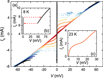
Figure 2. (a) A series of current–voltage characteristic (IVCs) for 12 different bath temperatures Tb = 8 K and from 12 to 25 K. From 12 to 18 K Tb is increased in steps of 2 K, from 18 to 25 K Tb is increased in steps of 1 K. (b) IVC for Tb = 8 K. A voltage jump occurs when the bias current Ib exceeds the critical current Ic = 7.8 mA. A hysteresis is observed here, marked by dashed red arrows. The whisker returns to the zero-voltage state when Ib is decreased below 6.4 mA. (c) IVC with Tb = 23 K. In this temperature range, the IVC is nonlinear but continuous.
Download figure:
Standard image High-resolution imageAs shown in figure 2(b), in the IVC obtained at Tb = 8 K, an abrupt voltage jump occurs when Ib exceeds Ic = 7.8 mA. The critical current density jc is estimated to be around 5 × 10⁵ A cm−2. A hysteresis can be seen in the IVC when reducing Ib to values below Ic. The whisker re-traps into the zero-voltage state when Ib reaches the return current Ir = 6.4 mA. The voltage just above Ic is about 62 mV, which is much higher than any value that could be expected for a Josephson junction or for phase-slip centers, where the voltage jump should be well below twice the energy gap voltage. The type of hysteresis seen in figure 2(b) has been discussed a lot in the literature and appears as a result of hot spot formation [15, 16, 23]. Below the return current, the hot spot disappears.
Figure 2(c) shows an IVC at Tb = 23 K, where the IVC is nonhysteretic but nonlinear before it finally turns into the linear regime. This behavior is observed in the temperature range from 22 K to Tc, which we call the high temperature range.
To describe whether or not Joule heating is important in a current-carrying superconducting microbridge, the Stekly parameter  is introduced [24]. α is the ratio between the heat generated in the resistive state and the heat transferred to the bath, and it depends on jc, the normal state resistivity ρs, the heat-transfer coefficient h, the bath temperature and the ratio d between the cross section of the microbridge and its cooled perimeter. When
  , Joule self-heating dominates and destroys the superconducting state even at currents lower than Ic, inducing the bistability between Ic and Ir. For our sample this is the case at temperatures below 18 K. The Stekly parameter decreases with increasing Tb. When Tb approaches Tc, α becomes less than 1, and hysteresis or bistability disappears. For our sample, this is the case for temperatures above 21 K. For this temperature, using α = 1 and a whisker thickness of about 300 nm one finds a heat-transfer coefficient of 17 W cm−2 K, which seems reasonable.
In the temperature range Tb from 18 to 21 K, multiple branches can be seen on the IVCs. This is shown in more detail in figure 3. Except for the branches corresponding to the zero-voltage state and the normal state, there are three additional branches, labeled Branch-1, Branch-2 and Branch-3 in figure 3. Also these branches are hysteretic. For example, when Ib exceeds 4.45 mA on Branch-2, the IVC switches to Branch-3, with a voltage jump from 19.7 to 31.2 mV. When Ib is decreased immediately, the whisker continues to stay on Branch-3 and returns to Branch-2 when Ib becomes less than 4.25 mA.
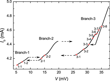
Figure 3. (a) Enlarged IVC at Tb = 20 K. Except for the zero-voltage state and the normal state, there are three more branches which are labeled by Branch-1, Branch-2 and Branch-3. Red circles indicate the bias points at which LTSLM is performed.
Download figure:
Standard image High-resolution imageThe additional branches and hysteresis can be induced by the formation of localized hot spots, appearing because of inhomogeneities, in our case the bending features of the whisker. Let us assume that a small hot spot has nucleated in the whisker for some reason. For a homogeneous sample, if the bias current is smaller than the so-called minimum normal-zone propagating current Ip [24], the hot spot will shrink again and disappear. If the bias current is larger than Ip, it will grow and eventually occupy the whole sample. However, if the sample is inhomogeneous because of the fabrication process, or because of the surrounding cooling environment, Ip(x) can become a function of the coordinate x along the whisker. Then, Ib might be larger than Ip at some position but smaller than the value of Ip(x) at other locations x. In this case, the hot spot would stay localized near the place x where Ib exceeds Ip(x). With increasing Ib it would expand along x, because the condition Ib > Ip(x) is fulfilled within a larger area.
To test these ideas, we use LTSLM to image potential hot spots caused by Joule heating. In figure 4 we show LTSLM images taken at the bias points (1-1) to (3-8) indicated in figure 3. The dashed lines indicate the boundaries of the whisker in the region between the voltage leads. Note that only in this region a voltage signal is picked up. In the LTSLM images at the two bias points (1-1) and (1-2) on Branch-1, the hot spot appears as the red feature at the right bottom of the bend in the whisker. The signal is quite localized and it is likely that the hot spot boundaries are not spatially resolved here. The hot spot expands towards the right electrode when Ib is increased from point (1-1) to point (1-2). In the LTSLM images at bias points (2-1) and (2-2) on Branch-2, the hot spot, or at least its left edge, appears at the upper end of the bend, i.e. its position differs from the one seen on Branch-1. ΔV(xL, yL) is large in the right half of the whisker, indicating that the whole bend is at a temperature near Tc. For bias point (3-1) on Branch-3, the left edge of the hot spot has changed its location again and appears near the left voltage electrode. With increasing Ib the left edge seems to leave the area between the voltage leads to the left, see bias points (3-2) to (3-5). At bias points (3-6) and (3-7), the sample area between the two voltage electrodes should be in the normal state, as suggested by the fact that the IVC is almost linear in this region. Indeed, the LTSLM signal is low. However, there seems to be some area close to the left voltage electrode producing somewhat higher values of ΔV, suggesting that in this region the local temperature is still close to Tc. At bias point (3-8), taken on the linear outermost branch of the IVC, the whisker is fully in the normal state and no strong LTSLM signal appears. This also holds for other bias points on the outermost branch (not shown).

Figure 4. LTSLM images taken at the bias points (1-1) to (3-8) indicated in figure 3. The dashed lines indicate the boundaries of the whisker in the region between the voltage leads.
Download figure:
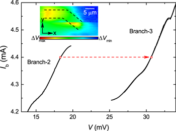
Standard image High-resolution imageWhen in the multi-branch temperature regime the whisker is biased near the end of a branch, the laser beam of the LTSLM can switch the IVC between different branches, as shown in figure 5. The bath temperature is Tb = 20 K and the sample is initially biased at 4.4 mA on Branch-2. The inset of the figure shows the LTSLM recording where the laser beam is moved line by line from bottom to top. The bias on Branch-2 is stable until the laser beam hits the hot spot, which is located near the bend, see figure 4. Then, the switch to Branch-3 occurs, and a further change of the laser position does not lead to a further switch of the hot spot position. The laser-induced switch is observable even for a very low laser power (less than 10 μW). The effect could be interesting for using the whisker as a photon detector or as a position-sensitive opto-electronic switch. The whisker is sensitive to laser beam irradiation at the location of hot spot, which in turn can be varied by the bias current. This may allow for more sophisticated configurations once a better understanding of the grown mechanism allows for controlling the shape of the whisker.
Figure 5. IVC at Tb = 20 K for currents between 4.2 and 4.6 mA. When biased at 4.4 mA, laser irradiation causes the whisker to switch from Branch-2 to Branch-3. The inset shows the LTSLM image taken during the switching event. Lower part: before switch, whisker located on Branch-2, upper part: after switch, whisker located on Branch-3.
Download figure:
Standard image High-resolution image
4. Conclusion
In this article we investigated the transport properties of a curved iron-based superconducting whisker. The resistive state is dominated by Joule heating, and no indications of, e.g. a Josephson-junction-like behavior or of phase-slip physics were found. Below the critical temperature, the resistive states of the sample can be divided into three temperature regimes. First, there is a low temperature regime where the sample immediately turns to the normal state because of strong Joule self-heating when the current exceeds the critical current. Here, the IVC is bi-stable. Second, there is an intermediate temperature regime with hysteretic multi-branch features in the IVC. LTSLM revealed that the multi-branch features arise from a localized hot spot which for different branches is located on different positions along the whisker. Finally, there is a high temperature regime close to the critical temperature where the IVC is continuous but nonlinear. Only here effects beyond Joule heating may be observable. In the multiple-branch region, the whisker can be switched between different states by a laser irradiating the hot spot, an effect which could be interesting for using the whisker as a photon detector or as a position-sensitive opto-electronic switch. More detailed studies of the performance of such devices, e.g. in terms of dark count rates and efficiency, are beyond the scope of the present paper but deserve future studies.
Acknowledgments
We gratefully acknowledge financial support from the National Natural Science Foundation of China (Nos. 61727805, 61611130069, 61521001, 11227904, 61501220, 61771234), innovative research team in university (PCSIRT) and Jiangsu Key Laboratory of Advanced Techniques for Manipulating Electromagnetic Waves. We also acknowledge support from the COST action NANOCOHYBRI (CA16218), and CAS Pioneer Hundred Talents Program.