

Abstract
Tailoring the properties of oxide-based nanocomposites is of great importance for a wide range of materials relevant for energy technology. YBa2Cu3O7−δ (YBCO) superconducting thin films containing nanosized BaHfO3 (BHO) particles yield a significant improvement of the magnetic flux pinning properties and a reduced anisotropy of the critical current density. These films were prepared by chemical solution deposition (CSD) on (100) SrTiO3 (STO) substrates yielding critical current densities up to 3.6 MA cm−2 at 77 K and self-field. Transport in-field Jc measurements demonstrated a high pinning force maximum of around 6 GN/m3 for a sample annealed at T = 760 °C that has a doping of 12 mol% of BHO. This sample was investigated by scanning transmission electron microscopy (STEM) in combination with electron energy-loss spectroscopy (EELS) yielding strain and spectral maps. Spherical BHO nanoparticles of 15 nm in size were found in the matrix, whereas the particles at the interface were flat. A 2 nm diffusion layer containing Ti was found at the YBCO (BHO)/STO interface. Local lattice deformation mapping at the atomic scale revealed crystal defects induced by the presence of both sorts of BHO nanoparticles, which can act as pinning centers for magnetic flux lines. Two types of local lattice defects were identified and imaged: (i) misfit edge dislocations and (ii) Ba-Cu-Cu-Ba stacking faults (Y-248 intergrowths). The local electronic structure and charge transfer were probed by high energy resolution monochromated electron energy-loss spectroscopy. This technique made it possible to distinguish superconducting from non-superconducting areas in nanocomposite samples with atomic resolution in real space, allowing the identification of local pinning sites on the order of the coherence length of YBCO (∼1.5 nm) and the determination of 0.25 nm dislocation cores.
Export citation and abstract BibTeX RIS
A correction was made to this article on 6 October 2015. The article title was corrected.
1. Introduction
Under specific conditions, high-temperature superconducting materials can carry electrical current with quasi zero resistance giving rise to a wide range of possibilities for technological applications in the areas of high-field magnets and energy, e.g. as power cables, transformers or current limiters [1, 2]. However, there is a great demand for further enhancement of the properties and reduction of fabrication costs of YBCO-coated conductors, which remain major challenges in applied superconductivity. Pinning centers impede the motion of vortices under a strong field gradient and, therefore, increase the critical current density Jc. A wide variety of defects can act as pinning centers in superconducting YBCO, such as twin boundaries, dislocations, and non-superconducting secondary phases. Although oxide-based nanocomposites are a developing research area little is yet known about structure-property correlations on the nanoscale [3]. Therefore, extensive research has been devoted to the study of magnetic vortex flux-pinning in high-Tc superconductors [1, 2, 4–8].
In recent years, chemical solution deposition (CSD) methods have been established as a viable route towards the fabrication of low-cost, highly efficient YBCO-coated conductors. Elaborate studies have been carried out on all-chemically deposited architectures of the superconducting film and suitable buffer layer systems by transmission electron microscopy (TEM) [4–12], scanning transmission electron microscopy (STEM) in combination with electron energy-loss spectroscopy (EELS) [13, 14], and electron tomography [13, 15]. Recent contributions on artificial pinning in CSD-derived YBCO films have shown that the pinning force can be greatly increased by the introduction of BaZrO3 (BZO) [16–23] or BaHfO3 (BHO) nanoinclusions [24]. BZO nanoparticles were reported to incorporate incoherently into the superconducting matrix and a strong isotropic flux pinning was observed [22]. However, the fundamental mechanism of pinning and a thorough structure-property correlation on the nanoscale still remains open. Even though a wide variety of related superconductor-insulator interfaces and pinning-relevant defects have been extensively studied, the actual pinning strengths, the strain fields of these artificial pinning centers, and the type of crystal defects they generate have not been studied in complete detail [21]. Recent work by Gutiérrez et al [16] proposes strain-driven broken twin boundary coherence as a relevant mechanism for pinning in YBCO nanocomposite thin films in which crystal defects play an important role.
Spatially resolved spectroscopy techniques are powerful tools to further address these issues. High spatial resolution maps of the superconducting behavior have been obtained from high-resolution scanning tunneling spectroscopy (STS) by Derro et al [48]. EELS in the TEM was used as a high spatial resolution method for analyzing the electronic structure of high-Tc YBCO thin films as early as 1991 by using the oxygen pre-peak as a position-sensitive probe of hole density by Eibl et al [41]. Similar experiments on the atomic scale have been performed by Song et al [49], but the focus in that case was on enhancing the critical current density at low-angle grain boundaries by Ca doping. The goal of the present work, however, is to increase understanding of the origin Jc enhancement due to artificial pinning sites in CSD-prepared YBCO thin films. On one hand it is known that strain fields around dislocations reduce the critical current density, and on the other hand they act as pinning sites, because their size is on the order of the coherence length of YBCO. The novelty in this work is that structural analysis on the atomic scale of artificial pinning sites is combined with spectroscopic analysis on the same scale in the above-mentioned sample type. The results of the combination give insight into the influence of defects on the macroscopic transport properties.
2. Experimental
YBCO nanocomposites with 12 mol% BHO were obtained via the trifluoroacetate metal–organic deposition (TFA-MOD) route described in detail in [25], but with one modification: ethanol was used as solvent for the precursor salts instead of methanol. The applied precursor solution was complemented with 12 mol% Hf(IV)-2, 4-pentanedionate with respect to yttrium as well as an equal amount of Ba(II)-trifluoroacetate for compensation. This solution was deposited on (100)-oriented STO single crystal substrates and subsequently annealed at temperatures ranging from 730 to 800 °C in an atmosphere of humid nitrogen with 100 ppm O2. The sample chosen for this detailed microscopy study was annealed at T = 760 °C with a doping of 12 mol% of BHO and presented the best pinning force density.
For electrical transport measurements, 50 μm wide bridges were prepared by wet-chemical etching after photolithographic masking. The transport measurements were performed in a four-probe configuration (i.e. Jc(B, 77 K), Jc(Θ) at several fields and temperatures, and R(B, T)) on selected samples on a physical properties measurement system (PPMS; Quantum Design, 1 μV criterion) and yielded critical current densities (Jc) of >3.6 MA cm−2 at 77 K in self-field. The maximum pinning force measured for the YBCO-nanocomposites was 6 GN m−3 at 0.8 tesla. Pure YBCO does not exceed 1.5 GN m−3.The angle Θ is spanned between the field B and the YBCO lattice parameter c with the rotation axis along the sample bridge and therefore along the applied current (maximum Lorentz force measurements). Irreversibility fields Birr were estimated with a Jc criterion of 100 A cm−2. For angular dependent measurements, the maximum Lorentz force setup was used, rotating the sample along the axis parallel to the electrical current. The resistive in-field measurements were carried out up to 9 tesla.
Cross-sectional specimens for (S)TEM were prepared by a combination of in situ focused ion beam and conventional Ar+ ion milling. High-angle annular dark-field (HAADF)–STEM image acquisition was carried out using an aberration-corrected (probe mode) transmission electron microscope 'TITAN Cube' operating at 300 kV (FEI Europe NanoPort—Eindhoven). For HAADF-STEM imaging at 300 kV an inner collection semi-angle β of 50–200 mrad was used. The acquired images were Fourier-filtered to reduce the noise. Java version 4.2231U2014 of the EMS code [26] was used to fit diffractograms and determine the orientation of the YBCO matrix and BHO precipitate. EELS data acquisition, processing and extraction: EELS data was acquired in an aberration-corrected FEI Titan 80–300 Cubed (S)TEM operating at 120 keV electron energy to maximize the interaction cross-sections, yielding a high signal-to-background ratio. Care was taken to choose the optimal acquisition conditions to minimize electron beam damage. The microscope was also equipped with an electron monochromator, increasing the energy resolution to 0.2 eV. EELS spectra were recorded on 2048 channels with an energy dispersion of 0.1 eV/channel in order to access information on most of the relevant elements simultaneously on a high-resolution Gatan GIF Quantum spectrometer. The convergence semi-angle was 18 mrad, the collection semi-angle was 59 mrad, the energy resolution was 0.2 eV, and the pixel dwell time was 0.05 s. EELS maps were generated by plotting the intensity under the corresponding background-subtracted EELS edges using the Digital Micrograph software package. Spectrum image filtered elemental maps were processed to reduce the detector noise with principal component analysis (PCA) [27], using 3–7 principal components. Care was taken that the application of PCA was only increasing the contrast in the elemental maps and not altering it or introducing artifacts.
Simulations of misfit edge dislocations at the YBCO-BHO interface were carried out using isotropic elasticity theory [28]. For simplicity it is assumed that misfit edge dislocations lie in bulk YBCO material. The relevant quantities for calculating the dislocation strain field are the length of the Burgers vector b and the Poisson ratio ν, which were calculated from the Young's modulus and the shear modulus. In our case the Burgers vector in YBCO was of type [100] and the Poisson ratio of YBCO ν = 0.086 [29]. Superconducting YBCO crystallizes in an orthorhombic crystal structure that has the space group Pmmm and lattice constants a = 3.8178 (1) Å, b = 3.8845 (1) Å, c = 11.6817 (3) Å. The non-zero elastic constants for YBCO (in GPa) are [29]: C11 = 230, C22 = 185.5, C33 = 111.21, C12 = 104.82, C13 = 50.17, C23 = 54.89, C44 = 42.31, C55 = 21.51, and C66 = 101.36. BaHfO3 has a cubic perovskite lattice structure and has a lattice constant of a = 4.2858 Å. The non-zero elastic constants (in GPa) are [30]: C11 = 313.18, C12 = 63.49, and C44 = 70.33. This is important for the dislocation orientation, i.e. where the extra half-plane is inserted. Because YBCO is the softer material (in terms of rigidity) additional half-planes are expected to be inserted more easily. A digital micrograph geometric phase analysis (GPA) plugin of Koch [31, 32] was used to extract the single strain tensor components from atomic resolution HAADF-STEM images. When this was not possible the local lattice deformation and rotation were determined [33, 34].
The Ti diffusion process was modeled by assuming an infinite extended STO/YBCO interface and both materials extending to infinity in the perpendicular direction, which reduces the geometry to one dimension. It is further assumed that there is no Ti depletion in STO close to the interface. Then the concentration c(x, t) of Ti atoms at depth x and time t in YBCO can be written as
With c0 as the initial Ti concentration and D as the diffusion coefficient.
3. Results
3.1. Scanning transmission electron microscopy, geometrical phase analysis and electron energy-loss spectroscopy
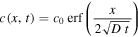
Figure 1(a) shows an atomic resolution HAADF-STEM image of a BHO nanoparticle located close to the STO substrate in the YBCO matrix. The corresponding crystallographic directions were extracted from the diffractogram (figure 1(b)) and are indicated in figure 1(a). In the right part of the BHO particle the BHO and YBCO lattice are overlapping forming a Moiré contrast. Figure 1(c) shows the  xx component of the strain tensor obtained using GPA analysis of figure 1(a) (the reflections used are indicated in figure 1(b)). Out of this image the dislocation core positions and orientations were determined and then used for the strain field simulation shown in figure 1(d). In both experiment and simulation, one dislocation was selected and magnified for comparison (see the insets in both images). The position and orientation of the extra half plane are indicated in the insets of the experiment and simulation images, respectively. Line profiles were extracted along the black arrow and plotted together in figure 1(e) to have a quantitative comparison. The dislocation core region is shown in gray and was defined as the region where the strain exceeds 20%. The core of the dislocations was determined to be about 0.25 nm in size.

Figure 1. (a) HAADF-STEM image of a BHO particle near the STO substrate interface. (b) FFT of (a) with indexed diffraction data of the YBCO matrix (red) and the BHO particle (blue). (c) xx strain component determined via geometric phase analysis [31, 32, 43]. The reflections used are indicated by the green circles in (b). (d) Simulated edge dislocation arrangement via linear elasticity theory according to (c). (e) Line profiles extracted from the indicated positions in (c) and (d), respectively. The number 1 in (a), (c) and (d) denotes a region at the YBCO/BHO interface, where in the experimental image the strain observed in the simulation was relaxed by introducing an Y-248 type of defect.
Download figure:
Standard image High-resolution imageFigure 2 is a HAADF-STEM image of a BHO particle in the YBCO matrix at atomic resolution. Note the sharp crystallographic facets of the BHO particle. The crystallographic orientation of the particle was again determined via the diffractogram shown in figure 2(b) and indicated in the image. The incorporation of the BHO particle into the YBCO matrix causes lattice defects like Y-248 intergrowths, which are also indicated in the image. The lattice deformation was calculated by determining the local variation (figure 2(c)) and rotation (figure 2(d)) of the g-vector indicated in figure 2(b). Due to Moiré effects the interior of the BHO particle shows a strong contrast. The Y-248 intergrowths can also be identified in the local g image (figure 2(c)).
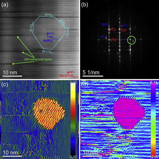
Figure 2. (a) HAADF-STEM image of a BHO particle in the YBCO volume. Note the sharp crystallographic facets with the indicated crystallographic indices. (b) FFT of (a) with indexed diffraction data of the YBCO matrix (red) and the BHO particle (blue). The local variation and rotation of the g-vector (indicated in (b)) determined via local geometric phase analysis [33, 34] are shown in (c) and (d), respectively.
Download figure:
Standard image High-resolution imageFigure 3(a) shows a HAADF-STEM image of a BHO particle inside the YBCO matrix. The region where an EELS map was acquired is indicated by the green rectangle. The unprocessed EELS map is shown in figure 3(b). Afterwards it was filtered using PCA to enhance the contrast and reduce noise (see figure 3(c)). To ensure that no artifacts were introduced during the PCA filtering, the region in the green square was chosen from figures 3(b) and (c), respectively, and plotted overlaid on each other in figure 3(d). Furthermore, the EEL spectrum extracted from the green square in figure 3(c) is plotted together with a similar sized area from the center of figure 3(c), i.e. from inside the BHO particle. The difference between the YBCO matrix and the BHO particle in the O-K edge and the O2p-pre-peak region can be seen directly from the EEL spectra, i.e. in the BHO particle there is no O2p-pre-peak because there are no empty states as in the YBCO. Additionally, a 2D STEM-EELS map was created in a similar way as described in [35]. The corresponding map was extracted from the red rectangle in figure 3(c) and plotted in figure 3(f). The line profile at the right side documents the decrease of the O2p-pre-peak intensity, i.e. the transition from superconducting parts of the sample into non-superconducting parts, when scanning the electron beam from the YBCO matrix into the BHO particle.

Figure 3. (a) HAADF-STEM image of a BHO particle in the YBCO matrix. (b) Principal component analysis using three components of the spectrum image. The red rectangle denotes the area where 2D STEM-EELS data were extracted. (c) Effect of the applied noise filtering procedure on EEL spectra including background. (d) Extracted EEL spectra at positions (1), i.e. YBCO matrix, and (2), i.e. BHO particle. Note the O2p-pre-peak intensity. (e) Complete 2D STEM-EELS data from (b) with line profiles documenting the O2p-pre-peak intensity. The x-axis units are electronvolts and the y-axis units are nanometers.
Download figure:
Standard image High-resolution imageFigure 4(a) shows a HAADF-STEM image of a BHO nanoparticle close to the STO substrate. The image was evaluated with respect to local lattice deformation and rotation [33, 34] documenting the strain being present in the lattice. The result is shown in figure 4(b). The numbers from 1 to 5 denote single edge dislocations with their associated strain fields at the YBCO/BHO interface. Figure 4(c) shows a color-coded O2p-pre-peak mapping of the nanoparticle region. Blue shades denote a low O2p-intensity, whereas reds indicate a high intensity. Figure 4(d) is an overlay image of figures 4(b) and (c), respectively. This was arranged to document the interplay of the dislocation strain field and O2p-pre-peak intensity, i.e. superconductivity on the nanometer scale. Figure 4(e) shows three EEL spectra extracted from the three magenta points in the O2p-mapping shown in figure 4(c). Even though BHO overlaps with the underlying YBCO in this area, the pre-peak signal is strongly diminished (see figure 4(e), blue spectrum). Again the transition from superconducting sample parts, i.e. YBCO matrix, to non-superconducting parts, i.e. BHO particles, is well documented by the decrease of the O2p-pre-peak intensity. The yellow arrows indicate the YBCO a- and c-axis directions at which line profiles of the O2p-pre-peak intensity were extracted, respectively. The result is shown in figure 4(f). The black curve shows the line profile along the YBCO a-axis and the red curve shows one along the c-axis. Notice that the transition region from superconducting to non-superconducting parts along the YBCO a-axis is about 2 nm wide. The single YBCO layers along the c-axis can be distinguished as oscillations of the O2p-pre-peak intensity, i.e. between copper planes and copper ribbons. The transition region at the substrate interface, i.e. where the O2p-pre-peak intensity is continuously decreasing, has a width of about 3 nm.
Figure 4. (a) HAADF-STEM image of a BHO particle close to the STO substrate. (b) Variation of the local lattice vector with edge dislocations on the YBCO film side indicated by the numbers. (c) O2p-pre-peak mapping: shades of blue indicate a low pre-peak intensity, and reds indicate high intensity. (d) Overlay of (b) with (c). (e) EEL spectra extracted at the magenta points in (c). (f) Line profiles along the yellow arrows indicated in (e).
Download figure:
Standard image High-resolution imageFigure 5 shows a color-coded 2D STEM-EELS measurement at the YBCO/STO interface. On the left side a simple atomic model of the analyzed area is shown next to the HAADF-STEM image. The line profile above the 2D STEM-EELS plot shows the EEL spectra of the three indicated lines (orange, magenta, and blue), respectively. Again the difference between copper planes (blue) and copper ribbons (magenta) can be identified. Also the YBCO/STO interface region (orange) can be identified. This observation is consistent with the O2p-pre-peak intensity line profile shown on the right side, which was extracted along the red rectangle from the 2D STEM-EELS data.
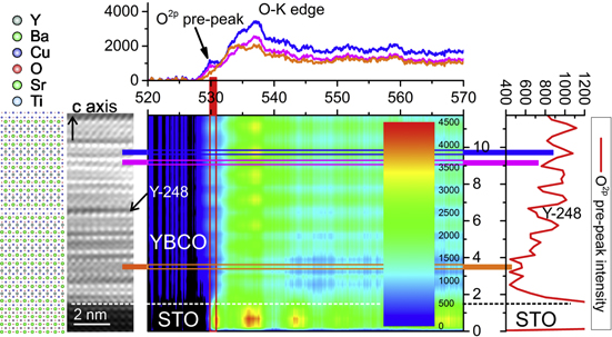
Figure 5. 2D STEM-EELS measurement close to the STO substrate and a BHO particle (not shown here). Note the variation of the O2p-pre-peak intensity along the c-axis. The x-axis units are electronvolts and the y-axis units are nanometers.
Download figure:
Standard image High-resolution imageFigure 6(a) shows a color-coded 2D STEM-EELS measurement at the YBCO/STO interface. On the left side a HAADF-STEM image is shown, and on the right side the O2p-pre-peak and the Ti-L2,3 intensity line profile are displayed in logarithmic scale for visualization purposes. These profiles were extracted along the red and magenta rectangles, respectively, from the 2D STEM-EELS data. Although it seems that the Ti signal oscillation into the YBCO bulk is periodic, which would suggest that the Ti diffuses into certain preferred atomic sites, we cannot be certain of this because we are close to the detection limit of the technique. This oscillation was not observed in the STO substrate. The line profile above the 2D STEM-EELS plot shows the EEL spectra of the YBCO and STO substrates, respectively. Figure 6(b) shows calculated diffusion profiles of Ti in YBCO for increasing diffusion times assuming an infinite Ti source in the negative part of the graph (STO substrate). The maximum diffusion time (60 min) is given by the annealing time of the film. The annealing temperature was 780 °C. However, the diffusion constant Dest = 1.5 × 10⁻⁴ nm s−1 had to be estimated by comparing the normalized EELS signal to the calculated diffusion curve for 60 min (see figure 6(c)), since no literature data for Ti diffusion in YBCO was available. This value is comparable to the impurity diffusion constants of Ba and Y in YBCO [36]. Other impurities such as Ni, Cu, Zn, Mg, Al, Ag, and Ca have diffusion coefficients at least by one order of magnitude larger than Ti [36, 37].
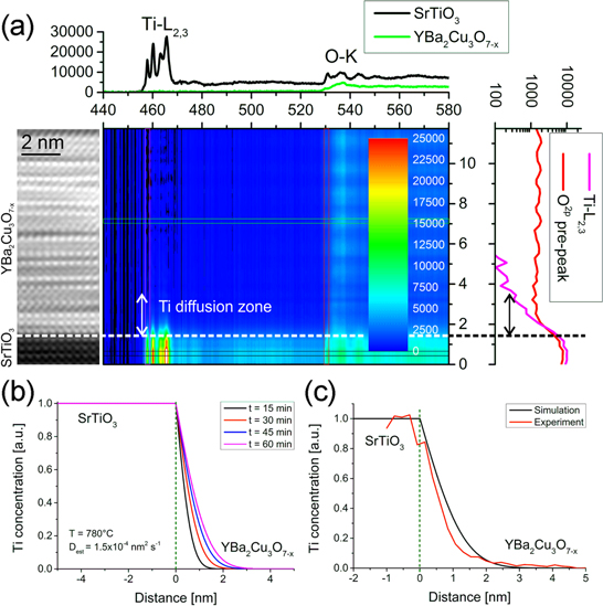
Figure 6. (a) 2D STEM-EELS measurement close to the STO substrate and a BHO particle (not shown here). Note the Ti signal reaching into YBCO film. The x-axis units are electronvolts and the y-axis units are nanometers. (b) Calculated Ti diffusion profiles at 780 °C into YBCO for various diffusion times assuming an infinite Ti source, i.e. bulk material. (c) Comparison of the calculated diffusion profile with the normalized EELS Ti-L2,3 signal. The diffusion constant D was estimated from the experimental profile due to the lack of literature values for Ti diffusion in YBCO.
Download figure:
Standard image High-resolution image3.2. Atomic scale image analysis by statistical parameter estimation theory
HAADF-STEM images were analyzed by means of statistical parameter estimation theory using the methodology presented by Van Aert et al [38]. The starting point of this method is the availability of a physics-based model describing the contrast of a HAADF-STEM image. Assuming a high-angle annular dark-field detector, an incoherent STEM image will be formed, which can be written as a convolution between an object function and the probe intensity. The unknown structure parameters of the object function, including the atomic column types and positions, are estimated by minimizing the uniformly weighted least squares criterion. By means of this procedure, atomic column positions can be estimated with high accuracy and precision. Distances between different columns were measured from the estimated atomic column positions in order to determine the distortion of the YBCO lattice caused by the BHO nanoinclusions.
Figure 7(a) shows an experimental image of an YBCO-BHO interface area. The measurement of the distances can be separated into two types: (i) the Ba-Cu-Ba (BCB) distance and (ii) the Ba-Cu-Y-Cu-Ba (BCYCB) distance. Table 1 shows the values obtained from crystallographic information together with estimated distances obtained from simulated and experimental images. Simulations of the YBCO and BHO lattices were carried out using the STEMsim program [39] using the crystallographic data as input. The second column of table 1 shows the estimated BCB and BCYCB distances obtained from such simulations. The third and fourth columns show the mean values obtained from areas of an experimental image selected near and far from the BHO particle, respectively. Some defects were detected due to the presence of the BHO precipitate. The local strain in the surroundings of the particles was quantified in a similar way to Cantoni et al [3] by measuring the variation  of the parameter in the YBCO lattice, where
  is the average measured parameter and c0 is the expected value of 11.68 Å from the crystallographic database. From this, it follows that the overall distortion of the YBCO lattice is 2% far from the particle and up to 7% near the particle.
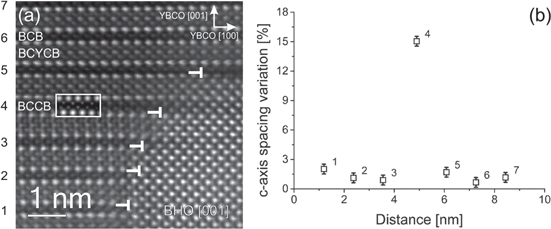
Figure 7. (a) HAADF-STEM image of an interface between the YBCO matrix and a BHO nanoparticle. A STEMsim [39] simulation is shown as an inset showing a Ba-Cu-Cu-Ba (BCCB) lattice defect structure with an extra Cu plane corresponding to Y-248 intergrowths [18]. A zig-zag arrangement of the Cu atoms is observed, which fits perfectly with the experimentally obtained image. (b) Measurement of the c-axis spacing variation in function of the distance.
Download figure:
Standard image High-resolution imageTable 1. Values of the interatomic distances measured from a simulation and from the experimental image shown in figure 3(a).
| Distance | Crystal Structure/Simulation | Far from particle | Near particle |
|---|---|---|---|
| BCB | 4.28 Å | 4.51 ± 0.02 Å | 4.92 ± 0.07 Å |
| BCYCB | 7.40 Å | 7.40 ± 0.05 Å | 7.34 ± 0.05 Å |
| c | 11.68 Å | 11.84 ± 0.04 Å | 12.40 ± 0.12 Å |
3.3. Superconducting properties
Figure 8(a) shows pinning force densities of a YBCO(BHO)/STO sample series prepared for the optimization of the annealing temperature. The optimum is found at 760 °C with a maximum pinning force density  of about 6 GN m−3. At higher and lower temperatures
  drops, but is still significantly higher than in films without artificial pinning centers throughout the entire temperature range investigated, since pristine films do usually not exceed 1.5 GN m−3. The film grown at 760 °C has been further investigated in angular dependent measurements (figure 8(b)), i.e. the angle of the magnetic field direction with respect to the c-parameter of YBCO and the rotation axis along the electrical current has been varied. A very low anisotropy of the critical current density is obvious at fields as low as 1 T at both temperatures applied. At 65 and 77 K, respectively, Jc values for B||c achieve approximately 80% and 70% of the critical current densities for B||a/b. At higher fields (here demonstrated for 5 T), and in particular at temperatures close to Tc the ratios deteriorate to 55% at 65 K and 5% at 77 K.
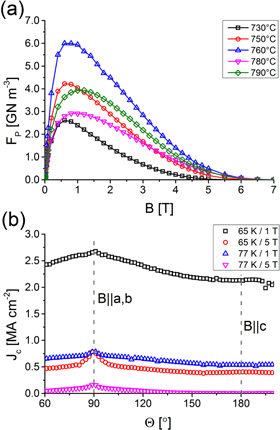
Figure 8. (a) Pinning force densities Fp(B) for samples of YBCO on STO containing 12 mol% BHO grown at different annealing temperatures. (b) Angular dependence of Jc for YBCO (BHO)/STO grown at 760 °C at two fields and two temperatures. The angle theta is spanned between the substrate normal and the magnetic field B with the rotation axis parallel to the electrical current.
Download figure:
Standard image High-resolution image4. Discussion
4.1. Methodology
4.1.1. Theoretical methodology
According to Fink et al [40] there are unoccupied states close to the Fermi level. The existence of these states originates from the amount of oxygen doping in the material; they do not occur in YBa2Cu3O6, but in YBa2Cu3O7. Fink et al [40] stated that these states are of type O2p and described their origin in detail. Since EELS is able to probe the electronic structure of a material, it can be used to detect those unoccupied states. Eibl et al [41] showed the potential of this method. The energy-loss near-edge fine structure (ELNES) of the O-K edge has, along with the characteristic peak located at an energy loss of 536 eV, an additional feature, called the pre-peak, located at 528.5 eV. The existence of this pre-peak in the EELS spectrum of YBCO depends on the presence of holes in the oxygen 2p band. Since these holes are the relevant superconducting charge carriers, this offers the possibility of distinguishing superconducting from non-superconducting regions [41]. Eibl et al [41] reported that they were able to map their samples with a lateral resolution of 10–50 nm. Electron microscopic and spectroscopic methods have since been greatly improved by the development of the spherical aberration corrector and a monochromator for the electron gun, improving lateral resolution to about 80 pm and spectral resolution to about 150 meV. Thus, this method is ideally suited to distinguish superconducting from non-superconducting regions on the atomic scale.
4.1.2. Experimental methodology
The schematic of figure 9 shows the methodology used for the analysis of strain fields of pinning active precipitates in YBCO superconductors. The starting point is aberration-corrected STEM. Two methods were used: atomic resolution HAADF imaging including image analysis (left) and EELS including ELNES analysis (right). The atomically resolved HAADF images were evaluated using GPA [31–33] in order to obtain the single strain tensor components (xx, yy, xy). If this method was not applicable, the local lattice deformation and rotation were determined [33, 34]. Both strain analysis methods lead to the quantification of the strain field on the nanoscale. The chemistry on the atomic scale was determined by acquiring EELS maps including the Ti-L2,3 and the O-K edge. These maps were evaluated with respect to the Ti distribution at the STO/YBCO interface yielding the Ti diffusion profile as well as O2p-pre-peak intensity yielding a fingerprint of superconductivity. In bulk, YBCO O2p-spectroscopy in the TEM was already carried out by Gauquelin et al [42]. However, their goal was not to map superconductivity in energy technology relevant samples on the atomic scale, but to determine the plane and chain contributions to the electronic structure in YBa2Cu3O6 and YBa2Cu3O7. If both methods are combined, i.e. HAADF-STEM imaging and EELS, it is possible to obtain an atomic scale map of superconductivity, i.e. it will be possible to identify pinning relevant structures.

Figure 9. Analysis procedure used to investigate TFA-MOD-derived YBCO thin films with BHO nanoinclusions by aberration-corrected scanning transmission electron microscopy.
Download figure:
Standard image High-resolution image
4.2. Observed strain fields and correlation with superconducting properties
The strain-fields of crystal defects associated with these pinning active BHO precipitates are known to be directly correlated to the augmentation of the superconducting properties in the system [18, 24] and were measured in this case quantitatively by high-angle annular dark-field (scanning) transmission electron microscopy in combination with GPA and statistical parameter estimation theory, thus allowing for the direct imaging and quantification of the corresponding strain fields. The in-plane and out-of-plane lattice mismatch values for BHO (+9.9 and +6.8) are similar to the BZO case (+8.3 and +7.1). The local lattice distortion matrix e is defined as given by Hÿtch et al [43] and the strain field matrix is obtained by taking the gradient of the displacement field. Our results show that the measured strain fields affect the lattice structure of YBCO within several nanometers from the crystal defect. Palau et al [44] have correlated the presence of BZO nanoparticles with the internal microstrain of YBCO-BZO nanocomposite superconductors by measurements using x-ray diffraction (XRD). Using the Williamson-Hall method, the internal microstrain in an YBCO layer, , could be determined. It has been proposed that the high enhancement of the isotropic Jc is mainly due to the contribution of the BZO nanoparticles located in the bulk of the films and to a lesser extent to interfacial nanoparticles, which mainly enhance the anisotropic Jc contribution [44]. This methodology contributes greatly to a direct microscopic correlation of microstrain and critical current enhancement, but is limited in providing an understanding of what actually occurs on the atomic scale. Also, the interaction between solution-derived BZO nanodot interfacial templates and YBCO films leading to enhanced critical currents has been studied by Abellan et al [45] and the role of various interfacial defects has been discussed in the literature [46]. A pinning landscape analysis in YBCO films has been shown in films with epitaxial and non- and/or semi-coherent nanoparticles [44]. However, a strain analysis on the nanoscale, i.e., structure-property correlation, is lacking. The tools and methodology presented in this contribution allow for the quantification of nanoscale strain-fields due to pinning active defects in YBCO superconductors.
We have shown that BHO nanocomposite YBCO thin films have a significantly increased pinning force as well as a critical current density compared to pristine YBCO films. The influence of different kinds of defects on the critical current density and pinning force in a BZO-doped YBCO sample was extensively discussed by Maiorov et al [20], Mastumoto and Mele [21], and MacManus-Driscoll et al [19]. Similar arguments hold, of course, for our BHO-doped sample. We furthermore directly prove the influence of the defects on the fundamental superconducting property of YBCO, i.e. the empty O2p states, by EELS on the atomic scale. A drastically improved pinning force density and high irreversibility fields in the YBCO layers containing nanosized BHO particles prepared by the trifluoroacetic acid process were also reported by Engel et al [24]. It was shown that the level of Hf doping in the precursor solutions results in an increased BHO nanoinclusion content. Investigations into the behavior of the critical current density in magnetic fields up to 9 tesla revealed a strong enhancement of Jc at high magnetic fields with an increasing amount of BHO precipitates. XRD measurements demonstrated the dependence of (i) the critical temperature Tc and the transition width ΔTc on the c-axis parameter of YBCO and (ii) the BHO content on the amount of Hf in YBCO. The Hf concentration was, therefore, correlated to the pinning force and the increased critical current density. This is also related to the increase in the density of Y-248 intergrowths [18]. Although both the lattice parameter and the BHO content increase simultaneously with increasing hafnium content, no significant change in the Tc values was detected. The concentration of Hf ranged up to 2 at.%, yielding an averaged c-axis parameter of more than 11.68 Å. In the case of the sample investigated in this work, the Hf content was increased up to 12 mol%, and the resulting c-axis lattice parameter changes measured locally by quantitative electron microscopy yielded values of 12.40 ± 0.12 Å and 11.84 ± 0.04 Å, respectively, corresponding to areas near and far from the BHO particle. The results are in good agreement with the values found by XRD studies [24]. A direct structure-property correlation (strain) on the nanoscale could be demonstrated and an effective methodology has been implemented for the analysis of nanoscale strain fields of pinning active precipitates in YBCO structured superconductors.
4.3. Influence of Ti diffusion
In a related contribution, Erbe et al [47] investigated TEM lamellae of YBCO thin films on STO without Hf addition via energy-dispersive x-ray (EDX) line scans and found the YBCO matrix to be contaminated by titanium throughout the entire thickness of the layer. This effect set in at annealing temperatures as high as 750 °C and increased gradually with increasing temperatures leading to massive effects on both Tc and Jc. They also reported that the influence of the STO substrate on Tc and Jc was much less obvious in films containing artificially forced BHO particles, and assumed that those particles could counterbalance the loss of the chemical inertness of the substrate at high annealing temperatures. Our own EELS measurements confirm that Ti is also diffusing into the YBCO matrix in films BHO containing; however, the interdiffusion layer is limited to a few nanometers. In the Ti diffusion zone we also observe a breakdown of superconductivity via the O2p-analysis technique, i.e. in BHO there is no O2p-pre-peak since there are no empty states as in YBCO. The amount of Ti diffusion is less in BHO than in YBCO, letting the BHO particles act as a diffusion barrier.
5. Conclusion
This contribution presents a detailed microstructural and chemical investigation of composite thin films of superconducting YBCO doped with nanosized BHO particles on STO substrates. A major objective was to use atomic-resolution Z-contrast STEM imaging and EELS mapping, including Ti chemical maps and O K-edge pre-peak intensity maps, to probe superconducting areas using the oxygen pre-peak of the O-K EELS signal along with a strain analysis around YBCO/BHO interfaces. The sample annealed at T = 760 °C was prepared by a TFA-MOD CSD process and 12 mol% of BHO doping was selected according to optimized deposition parameters and superconducting properties (Jc, Jc anisotropy, and field-dependent pinning force). The first part is to image pinning-relevant structures at atomic resolution with STEM-HAADF images, i.e. strain mapping, whereas the second part probes the local electronic structure and charge transfer by high energy-resolution monochromated electron energy-loss spectroscopy, i.e. spectral mapping. This technique allowed distinguishing superconducting from non-superconducting areas in nanocomposite samples with atomic resolution in real space, allowing the identification of local pinning sites on the order of the coherence length of YBCO (∼1.5 nm) and the determination of dislocation cores of size 0.25 nm. Furthermore, we document Ti diffusion from STO into YBCO due to the elevated processing temperatures by using EELS. We report a direct observation and quantitative analysis of interfacial misfit edge dislocation arrays in YBCO-BHO nanocomposite superconductors by HAADF-STEM. Two types of local lattice defects were identified and imaged: misfit edge dislocations and Ba-Cu-Cu-Ba stacking faults (Y-248). Misfit interfacial dislocations were identified at the BHO-YBCO interface, distance less than 2 nm. A model-based analysis that relies on fitting the contrast of individual atomic columns was used to measure local atomic displacement and was found to be suitable for measuring displacements at the highest possible resolution. Sharply facetted BHO nanoparticles coherent to the YBCO matrix were found, and the termination edges of the facets act as nucleation centers for Y-248 intergrowth formation. It remains to be found what drives coherency and whether coherent and incoherent particles coexist.
Acknowledgments
The authors acknowledge financial support from the European Union under the Framework 6 program as a contract for an Integrated Infrastructure Initiative (References No. 026019 ESTEEM) and by the EU-FP6 Research Project 'NanoEngineered Superconductors for Power Applications' NESPA no. MRTN-CT-2006-035619. This work was supported by funding from the European Research Council under the Seventh Framework Programme (FP7). LM-L, ST and GVT acknowledge ERC grant No. 246791—COUNTATOMS and funding under a contract for an Integrated Infrastructure Initiative, Reference No. 312483- ESTEEM2, as well as the EC project EUROTAPES. GTM and SVA acknowledge financial support from the Fund for Scientific Research-Flanders (Reference G.0064.10N and G.0393.11N). MD acknowledges financial support from the LOEWE research cluster RESPONSE (Hessen, Germany). ME has received funding from the European Union Seventh Framework Programme (FP7/2007–2013) under grant agreement no. NMP-LA-2012-280432. LM-L and MD kindly acknowledge support from Professor H-J Kleebe to complete this investigation.