
Abstract
Highly textured transparent conducting front electrode (TFE) can enhance light trapping; however, we observed an improved performance of a solar cell by nanometer level modification of surface texture. A 40 nm thick aluminum doped zinc oxide was sputter deposited at an oblique flux on the textured fluorine doped tin oxide TFE, and a TFE double layer was used for the front electrode of solar cells. The cells fabricated on these modified TFEs exhibited an increased open circuit voltage, enhancement in short circuit current density and an increase in fill factor that reached up to 74% because of reduced series resistance of the cell. The surface texture of the TFE was modified with various angular fluxes of the zinc oxide sputter particle, which shows lower texture-induced-surface defect, higher work function. These are thought to have helped in improving the performance of the thin-film solar cells. However, at a near normal angular flux of the zinc oxide sputter particle, light trapping was observed to have reduced significantly, leading to a significant reduction in current density of the cell.
Export citation and abstract BibTeX RIS
1. Introduction
Photovoltaic conversion efficiency of an amorphous silicon solar cell can be enhanced with the introduction of light trapping scheme. The diffused transmission at the front surface [1] and its reflection at the back [2, 3] can lead to a significant improvement in the short circuit current density (Jsc) [4, 5]. In order to obtain better light trapping, higher roughness of the textured surface can be adopted. However, while the thin layers of the solar cells were deposited on a deeply textured transparent conducting oxide (TCO), a poor localized surface contact between the p-layer and the TCO may be formed at some points over the surface. From the optics point of view, an enhanced parasitic absorption has been reported for cells with higher surface texture [6]. Furthermore, the energy band structure between the TCO and the p-layer is another important aspect of the solar cell [7], as the front interface may behave like a Schottky junction if the difference in work function between the layers is significant. Based on the Richardson's thermionic equation, larger difference in Fermi energy between the TCO and p-layer can lead to low current density across the TCO/p interface, resulting in low fill factor (FF) of the cell and hence reduced cell efficiency. The fluorine doped tin oxide (FTO) has lower work function in comparison to that of the aluminum doped zinc oxide (AZO). In our investigation, we deposited a thin AZO layer over the textured FTO, investigated the cell characteristics and observed an improvement in solar cell parameters.
2. Experimental description
Initially we deposited several AZO single layers on Corning (Eagle XG) glass substrates by dc magnetron sputtering (MS) of 2 wt.% Al2O3 doped ZnO target, with 2 mTorr deposition pressure, 15 sccm Ar gas flow rate, 2.74 W cm−2 dc power density of the plasma, 155 °C substrate temperature and 5 rpm angular speed of the substrate and characterized the AZO films. We varied the target angle (θ) of the MS system to obtain various surface textures and work functions; here the θ = 90° indicates that the target and substrate surfaces are parallel and facing each other. A schematic diagram of the target-substrate orientation of the MS system is shown in figure 1. Accessing various points of the rough surface was one of the reasons for using various angular fluxes of AZO sputter particles. We used a commercially available ∼650 nm thick textured FTO coated glass substrate, deposited a 40 nm thick AZO over it, and fabricated solar cells on the modified TFE. Prior to the deposition, the substrates were cleaned ultrasonically in acetone and isopropyl alcohol for 10 min, rinsed with de-ionized water, and dried in N2 gas. A pre-sputtering on the AZO target was carried out for 5 min before the film deposition. The mobility and concentration of the charge carriers in the AZO films were measured by the Hall effect measuring instrument (model: ECOPIA HMS-300).
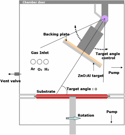
Figure 1. Schematic diagram of the magnetron sputtering system for the AZO layer deposition, where the target angle with reference to the substrate can be altered.
Download figure:
Standard image High-resolution imageThe amorphous silicon layers of the solar cells were deposited in a cluster-type multi-chamber plasma enhanced chemical vapor deposition system at 13.56 MHz (for the p-type layer and n-type layer deposition) and at 60 MHz (i-type layer deposition) plasma frequency. The solar cell structure was: glass/FTO(650 nm)/AZO(40 nm)/p-a-SiC:H(15 nm)/i-a-SiC:H(5 nm)/i-a-Si:H(400 nm)/n-a-Si:H(10 nm)/n-µc-Si:H(20 nm)/Ag(100 nm)/Al(1 µm), where p-a-SiC:H is the p-type hydrogenated amorphous silicon carbide (a-SiC:H), i-a-SiC:H the intrinsic a-SiC:H buffer layer, i-a-Si:H the intrinsic-type hydrogenated amorphous silicon (a-Si:H), n-a-Si:H the n-type a-Si:H, and n-µcSi:H the n-type micro-crystalline silicon layer. We used B2H6 (2% doping) and PH3 (3% doping) as the p-type and n-type dopant gas, respectively. A schematic diagram of the solar cell is shown in figure 2.

Figure 2. Schematic diagram of the solar cell structure. The dimensions are not to scale. The gap in the textured FTO and AZO symbolizes the 'cavity'-type surface defects.
Download figure:
Standard image High-resolution imageThe total and diffused transmittance of the TCO layers was measured with the help of an integrating sphere. The external quantum efficiency (EQE) was measured in an EQE measuring system (model: QEX7, PV Measurement Inc.). Images of the TCO surfaces were recorded in a scanning electron microscope (SEM). The current density–voltage (J–V) characteristics of solar cells were measured under 100 mW cm−2, with AM 1.5 illumination, and at 25 °C cell temperature. We investigated three cells for each set of the textured front electrode.
A numerical simulation was carried out with the help of AFORS-HET computer program (freely available at www.helmholtz-berlin.de/f o rschung/e n m a/s i-p v/p r o j e k t e/asicsi/afors-het/index_en.html). The properties of layers of the solar cells were kept constant during simulation, while the series resistance (Rs) and parallel resistance (Rp) were changed to fit the theoretical current voltage (LIV) characteristics of the cells under illumination, with that of the experimental LIV results. In this way we estimated the Rs and Rp through the simulation.
3. Results and discussions
The AZO layers that we deposited and investigated had the mobility of charge carriers 15 cm2 V−1 s−1, carrier concentration 5 × 1020 cm−3, resistivity 10−3 Ω.cm. Figures 3(a) and (b) show SEM surface images of FTO without the AZO layer. Here sharp edges and tips of the individual (nearly pyramidal) surface structure are visible; these have lateral dimension within 100 nm to about 1 µm. Figures 3(c)–(g) show that, after the AZO layer deposition at various θ, the edges of the pyramidal structures became less sharp. The surface roughness of the textured FTO and FTO/AZO double layers were nearly 150 nm, except that of θ = 72.5°, which is about 90 nm.
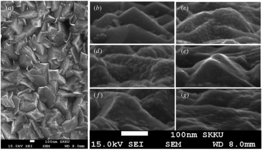
Figure 3. SEM surface image of (a) top view of textured FTO, (b) inclined view of textured FTO, and (c)–(g) inclined view of the 40 nm AZO coated textured FTO surfaces where the AZO layers were deposited with various θ, (c) θ = 32.5°, (d) θ = 40.0°, (e) θ = 47.5°, (f) θ = 65°, (g) θ = 72.5°.
Download figure:
Standard image High-resolution imageYablonovitch and Cody [8] proposed that, in an ideal light trapping, with random statistical light, the absorption coefficient of cell material enhances by 4n2 times, where n is the refractive index of the material. As higher diffused transmittance through the front surface implies increased randomness of light inside the cell, it is expected that, for a relatively higher diffused transmission through the TFE, the absorption coefficient of the cell active layer will increase. The diffused transmission is shown in figure 4(a), the inset shows total transmittance spectra. Figure 4(b) shows the difference in diffused transmission as well as total transmission spectra of the FTO/AZO double layers, with reference to that of the FTO film (without the AZO layer). A reduction in diffused transmittance at wavelength λ < 400 nm, and total transmittance at λ < 600 nm was observed. When the AZO layers were deposited on the FTO, the difference in the total transmittance of the TCOs was significantly lower (within 300–500 nm wavelength range), whereas a relatively smaller reduction was observed for λ > 500 nm. Light trapping is useful for longer wavelength of light where absorption coefficient is low. However, as total transmittance of light shows small reduction, due to the presence of the AZO layer, it is expected that the current density of the cells will reduce, although an increase in diffused transmission may help in enhancing the current density. The effect of light trapping has been estimated with the help of the EQE spectra. Based on the Schades and Smith model, the EQE can be expressed as [9, 10]

where RF is the reflectance of the top surface of the cell, A is the absorbance while its subscript indicates the concerned layer, ϕ is the EQE enhancement factor, which in an ideal situation is considered unity. The Jsc can be expressed as

where q is the electronic charge, h is the Plank constant, c is the speed of light, and χ(λ) is the AM1.5 solar spectra.
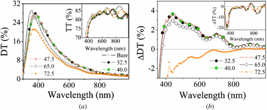
Figure 4. (a) Diffused transmittance (DT) and total transmittance (TT) (in the inset) of FTO/AZO double layer. The legend 'bare' indicates FTO without the AZO coating, while the numbers indicate the θ with which AZO layers were deposited. (b) Difference in diffused transmission (ΔDT) of the FTO/AZO double layers with reference to that of the textured FTO film. The inset shows a similar difference in total transmittance (ΔTT).
Download figure:
Standard image High-resolution imageWith reference to the cell without AZO, the EQE of all the cells (not shown here) with an FTO/AZO double layer showed a small reduction in blue response for λ < 450 nm, and a small enhancement for λ ∼ 620 nm; except for the last cell (AZO deposited at θ = 72.5°), the EQE decreased significantly for λ > 450 nm. We estimated ϕ using equation (1) (figure 5(a)) for all the solar cells. A small reduction in ϕ for λ < 600 nm is thought to be due to reduced optical transmission through the double layer front TCO (figures 4(a) and (b)), although it is expected to improve if thinner FTO were used. A marginal increase in ϕ for λ ∼ 650 nm, for the cells with the additional AZO front layer, may not have a significant impact on the cell performance. For the last cell (with θ = 72.5°), a drastic reduction in light trapping becomes visible for λ > 500° nm, possibly due to the additional reduction in diffused transmission with the AZO layer, as indicated in figure 4(a). This figure shows that thickness and texture dependant optical transmission of the TCO plays a significant role in light trapping.

Figure 5. (a) Spectra of EQE enhancement factor for the cells, here 'phi' indicates ϕ of equation (1). (b) Energy band diagram of the layers used in fabricating the solar cells, where EF is the Fermi level; VB the valence band; Ec the conduction band edge, top most dotted line is vacuum level; Vb1, Vb2 are the expected built-in potential in the cells before and after use of AZO, respectively.
Download figure:
Standard image High-resolution imageFor θ < 72.5°, there is a small reduction in light trapping with the introduction of the 40 nm AZO layer. Figure 5(b) shows the energy band structure of the materials used in solar cell fabrication. In order to simplify band structure analysis, we divide the cells into two components: a Schottky diode, formed by the TCO/p combination, where majority carrier transport follows Richardson's thermionic equation J = AGT2 e−W/kT; here AG is the Richardson constant, T the temperature, and W the work function difference of the layers. The other part of the cell follows the semiconductor diode equation. The measured FTO work function was 4.3 eV while that of the AZO films were 4.7, 4.71, 4.76, 4.89, 5.72 eV for the AZO films deposited at θ = 32.5°, 40.0°, 47.5°, 65.0°, 72.5°, respectively. Thus, the higher work function of the AZO layers may reduce the Schottky barrier, leading to an increase in current density through the TCO/p interface. This, as well as an increase in open circuit voltage (Voc), is reflected in the light induced J–V characteristics of the cells as shown in figure 6(a). The increase in Voc is indicated by Vb1 and Vb2 in figure 5(b).

Figure 6. (a) J–V characteristics of solar cells having different AZO interlayers, with the legends as explained earlier. (b) Comparison of experimentally observed Jsc (ExptJsc) to that estimated from EQE spectra (EQEJsc), using equation (2). The cell numbers 0,1,2,3,4,5 correspond to 'bare', θ = 32.5°, 40.0°, 47.5°, 65.0°, 72.5°, respectively. The cell number 0 is taken as reference.
Download figure:
Standard image High-resolution imageWe observed that Jsc of most of the cells remain higher with reference to the cell having no AZO in the front electrode, except for the cell with ϕ = 72.5°, figures 6(a) and (b). In figure 6(b) 'EQEJsc' was estimated by using equation (2). Among the investigated cells (three sets of cells for each θ), we measured the highest Jsc as 15.2 mA cm−2 and efficiency (η) as 9.7% (for θ = 47.5°), and FF as 74.4% (for θ = 72.5°). The reduced Jsc and η for the last cell may be because of the reduced light trapping, figure 5(a). The experimentally observed Jsc remains higher than that estimated from the EQE spectra, probably because of the reduced Schottky barrier height at the TCO/p interface of the cells with the AZO layer, in comparison to the cell having no AZO. The FF and Voc of all the cells showed marked improvement.
One more reason for such an improvement in solar cell performance may be attributed to the reduced localized surface defects at the TCO/p interface due to the AZO layer. The side view of the FTO/AZO double layers was investigated under SEM. It revealed that some nano cavity or texture induced localized surface defects were formed between the AZO and FTO, at the deep trough between the neighboring pyramidal textures of the FTO (figure 7(a)), leading to a localized poor electrical connection between the FTO and the p-layer (figure 7(b)).

Figure 7. (a) Side view of the 40 nm AZO layer deposited over a textured FTO surface, showing a nano cavity formed at the trough of two neighboring pyramidal textures. One side of the triangular cavity is about 30 nm. (b), (c) Schematic demonstration of reduction of texture-induced defects by the AZO layer deposition. (b) Defective TCO/p contact formation by p-layer deposition, (c) improved TCO/p contact due to the presence of AZO inter layer. Here dimensions are not to scale.
Download figure:
Standard image High-resolution image
A schematic demonstration of this phenomenon has been shown in figures 7(b) and (c). Figure 7(b) shows that the deposition of p-layer over the textured FTO will most likely form a 'cavity'-type defect. With the AZO layer deposition, the electrical connection between the defective part of the p-layer and the TCO could be established. Thus, the localized surface defects could be reduced.
Another reason for such an improved FF and Voc of the cells with thin AZO might be attributed to the improvement in the transparent conducting properties of the AZO due to hydrogen doping [11, 12], that may have happened during the p-layer deposition. However, under the hydrogen plasma the FTO surface probably becomes partially defective [13]. The improved TCO/p interface can also result in the reduction of series resistance (Rs) and interface defects. The reduced defects may also contribute to the improved Voc, the reduced Rs will result in increased FF.
4. Simulation
The AFORS-HET simulation shows that the Rs of the cell without AZO was 6.0 Ω.cm2. When the AZO layer was deposited with θ = 32.5° the result was Rs = 0.8 Ω.cm2, which was nearly the same for the rest of the cells, except for the last cell, Rs ≤ 0.1 Ω.cm2. The solar cell parameters used in the simulation are given in table 1.
Table 1. Some of the solar cell parameters used in the AFORS-HET simulation.
| Parameters | p-a-SiC:H | i-a-Si:H | n-µc-Si:H |
|---|---|---|---|
| Layer thickness (nm) | 15 | 400 | 20 |
| Dielectric constant | 11.9 | 11.9 | 11.9 |
| Electron affinity (eV) | 3.9 | 3.9 | 3.9 |
| Band gap (eV) | 1.82 | 1.52 | 1.52 |
| Optical band gap (eV) | 1.82 | 1.52 | 1.52 |
| Conduction band density of states (cm−3) | 4 × 10¹⁸ | 2.5 × 10¹⁸ | 4 × 10¹⁸ |
| Valence band density of states (cm−3) | 4 × 10¹⁸ | 2.5 × 10¹⁸ | 4 × 10¹⁸ |
| Electron mobility (cm2 V−1 s−1) | 1.5 | 10 | 0.5 |
| Hole mobility (cm2 V−1 s−1) | 0.37 | 1 | 0.1 |
| Thermal velocity of holes (cm s−1) | 106 | 7 × 10⁵ | 1 × 10⁶ |
| Thermal velocity of electron (cm s−1) | 4 × 10⁶ | 7 × 10⁵ | 5 × 10⁶ |
| Doping concentration (cm−3) | 6.9 × 10¹⁹ | 1000 | 7.5 × 10¹⁹ |
| Layer density (g cm−3) | 2.328 | 2.328 | 2.328 |
| Donor defect density (cm−3) | 5 × 10¹⁷ | 5.5 × 10¹⁶ | 6.9 × 10¹⁸ |
| Acceptor defect density (cm−3) | 5 × 10¹⁷ | 5.5 × 10¹⁶ | 6.9 × 10¹⁸ |
| Defect type | Gaussian | Gaussian | Gaussian |
| Electronic capture cross section of electron (cm2) | 3 × 10⁻¹⁵ | 3 × 10⁻¹⁵ | 3 × 10⁻¹⁵ |
| Electronic capture cross section of hole (cm2) | 3 × 10⁻¹⁴ | 3 × 10⁻¹⁴ | 3 × 10⁻¹⁴ |
Thus, the surface modification of the textured FTO glass, with the help of the AZO layer, might have reduced surface defects and Schottky barrier height at the TCO/p interface. Here, it seems that the change in the characteristic parameters of the cells was due to a combination of two effects, reduced texture-induced-surface defects and reduced Schottky barrier height at the TCO/p interface. It appears impossible to isolate the roles of these two effects on cell performance because both work function and reduction of texture-induced-surface defects are associated to the angle of flux of the AZO sputter particle towards the textured FTO substrate. However, in a different set of experiments the two effects may be separately investigated.
Here we have demonstrated that the texture induced 'cavity' defects can possibly be corrected well by sputter deposition of a thin transparent conducting layer, with nearly 47.5° angle flux of the sputter particle.
5. Conclusions
In summary, the sputter deposition with an angular flux of the AZO film over the textured FTO substrate helped to improve the short circuit current density and fill factor of the solar cell in two possible ways, such as reducing cavity-type surface defect and reduced Schottky barrier at the TCO/p interface. At various angular fluxes of the AZO sputter particle the change in surface texture varies, at a higher target angle the surface texture reduces. An optimum cell property was observed for θ = 47.5°, which may remain dependant on the nature of the surface texture; sharper texture may produce better results at a higher ϕ and vice versa.
Acknowledgment
This work was supported by the New and Renewable Energy of the Korean Institute of Energy Technology Evaluation and Planning (KETEP) grant funded by the Korean government Ministry of Knowledge Economy.