
Abstract
The evolution of luminescence properties and voids formation with respect to annealing temperature in H implanted ZnO was investigated by depth-resolved cathodoluminescence spectroscopy (DRCLS), transmission electron microscopy and secondary ion mass spectrometry (SIMS). The annealing temperature is found to induce noticeable changes to the shape, size and empty volume density of the cavities. DRCLS results also reveal that the green emission is influenced by different annealing temperatures. In particular, the 600 °C anneal produces a strong quenching of the green emission in the implanted region, while after the 800 °C anneal a significant enhancement near the surface is observed. The annealing at 600 °C also results in an uncommon violet emission at ∼3.1 eV that is not observed after a higher annealing temperature. A clear correlation between the violet emission, vacancies and Li is revealed from comparison between the DRCLS intensities and SIMS data.
Export citation and abstract BibTeX RIS
1. Introduction
ZnO is a direct wide bandgap (∼3.4 eV) semiconductor with an exciton binding energy of ∼60 meV. This is ∼2 times higher than GaN at ∼26 meV, thus making ZnO a very attractive alternative to nitrides for the fabrication of optoelectronic devices operating in the ultraviolet (UV) region. However, commercial use of ZnO based optoelectronic devices is still not available, as the fabrication of stable, reliable and reproducible p-type ZnO is still not achievable. Although hydrogen remains as a controversial impurity in ZnO, there is a general agreement both theoretically and experimentally that H plays a major role in the difficulty to achieve a p-type doping in ZnO [1–6]. A good understanding of H and its related defects in ZnO is crucial to obtain better control over the electrical conductivity of ZnO. Doping of H through ion implantation is an effective way to investigate the interaction between H and intrinsic defects in ZnO by exploiting the implantation damage.
Previously it has been shown that in ZnO implanted with 1 × 1017 cm−2 H− ions and annealed at 800°C for 1 h in air, the implanted region is decorated with voids the size of ∼2–30 nm [7]. In the present work, depth-resolved cathodoluminescence spectroscopy (DRCLS) is used to investigate the emission from H implantation induced defects in ZnO that is annealed at varying temperatures. The samples are also analysed by cross-sectional transmission electron microscopy (XTEM) and secondary ion mass spectrometry (SIMS) to correlate the distribution of the defects and impurities with respect to the DRCLS emission from the implanted region.
2. Experimental
Hydrothermally grown ZnO single crystals purchased from Tokyo Denpa Co. (Japan) were used in this study. 1 × 1017 cm−2 H− ions were implanted into the Zn (0 0 0 1) surface of the samples at 100 keV at room temperature. The H implantation was carried out with a tandem accelerator (NEC, 5SDH-4) that has a maximum terminal voltage of 1.7 MV. To minimize the effect from channelling, the samples were tilted 10° with respect to the incident beam during implantation [8]. After H implantation, the samples were annealed by a conventional furnace at 600 to 800 °C for 1 h in air. The implantation and impurity concentration profiles were measured by SIMS using a Cameca IMS 7f instrument. Crater depths were measured with a Dektak 8 stylus profilometer and a constant erosion rate was assumed when converting sputtering time to sample depth. Calibrations of H and Li were accomplished via ion-implanted reference samples.TEM analysis of the samples was carried out with a Philips CM300 instrument equipped with a LaB6 filament operating at 300 kV. DRCLS measurements were carried out at 80 K with a FEI Quanta 200 scanning electron microscope using incident excitation energies EB = 2 to 30 keV. The beam power was held constant at 15 µW at each EB by adjusting the beam current such that a constant power density was maintained at different sampling depths.
3. Results and discussion
3.1. Thermal evolution of microstructures and implanted H
After 600 °C annealing, a band of voids is observed at the peak of the as implanted H profile, as illustrated in the XTEM image in figure 1(a) and the SIMS results in figure 1(b). The as implanted SIMS H profile peaks at ∼670 nm, which is close to the SRIM simulated projected range Rp≈660 nm [9]. Significant outdiffusion of implanted H is observed upon annealing, with the peak H concentration decreasing to ∼0.2–0.4% of the initial concentration after 800 °C annealing [7]. SIMS measurements also show that upon annealing, Li redistributes to a profile that matches the shape of the H profile. The resemblance of the Li and H profiles suggests that (LiZn–OH) complexes form during thermal annealing, however the trapping of H and interstitial Li at the same acceptor-like defects cannot be ruled out [7]. The XTEM image in figure 1(a) also shows that the voids in the 600 °C samples are round and irregular in shape, in an obvious contrast to the sharp faceted voids observed in the 800 °C samples [7]. By sampling a defect free region in the XTEM images taken along [1
 0 0] (400 nm × 400 nm, with the centre at Rp) for each sample annealed at 600 °C and 800 °C, respectively, statistical analysis of the empty volume density and the voids sizes is carried out. By measuring 75 voids for each sample, the voids in the 600 °C sample are found to have larger sizes of ∼14 ± 9 nm, compared to ∼10 ± 5 nm in the 800 °C sample. Furthermore, by assuming the same thickness for both the XTEM foils, from an empty volume density measurement (total area of voids/total volume of the sampled area), the empty volume that is bound by the voids in the Rp region is estimated to be approximately three times larger in the 600 °C sample than in the 800 °C sample.
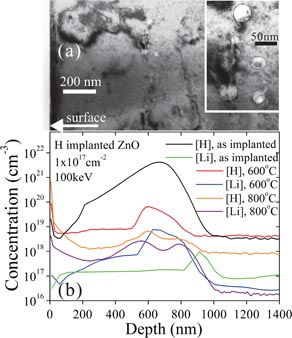
Figure 1. (a) Cross-sectional TEM micrograph along the [1 1
 0] zone axis of ZnO single crystal implanted with 1 × 1017 cm−2 H− at 100 keV and annealed at 600 °C. Inset shows a magnified TEM image of the voids. (b) SIMS profiles of H and Li in ZnO implanted with 1 × 1017 cm−2 H− before and after annealing at 600 °C and 800 °C.
Download figure:
Standard image High-resolution imageThe shrinkage in void size and a reduction in empty volume at >600 °C, as revealed by comparing figure 1(a) and the previous studies [7], corroborates the positron annihilation spectroscopy (PAS) data that exhibits a drop in the vacancy concentration in the H implanted region at temperatures >700 °C [10]. In hydrothermally grown ZnO samples implanted with Zn, upon annealing, mobile Zn interstitials (Zni) are observed to be released rapidly from the implanted region and 'kick out' substitutional Li from Zn sites (LiZn) [11]. This produces highly mobile Li interstitials (Lii) and results in a significant Li depleted region beyond Rp [11]. This was ascribed to being similar to the commonly known transient enhanced diffusion (TED) of B in Si [12]. The burst of Zni is reported to occur at temperatures ∼600–800 °C [11], and coincides with the temperature at which a decrease in void sizes is observed in the present work. As Zni are highly mobile even below RT [13], they are expected to participate in the annihilation of VZn. During annealing, the burst of excess Zni from the implanted layer further promotes the VZn annihilation process, thus causing a shrinkage in size of the voids in the present work, as well as the decrease in VZn concentration as reported by PAS studies [10]. However, in contrast to the Zn implanted samples, the SIMS result in figure 1(b) shows no depletion of Li in the implanted region. This could be due to the voids/bubbles formed in H implanted samples behaving as a strong sink for Zni, thus minimizing the impact of Zni on the Li profiles through TED as observed in Zn implanted samples [11]. In addition, it is also likely that Li atoms are decorating the voids and influencing their shapes, as fast diffusing metals are commonly known to accumulate around voids in Si [14–16]. For irradiated hydrothermally grown ZnO, PAS studies have also shown the trapping of Li in the vicinity of vacancy clusters after annealing [17]. Nevertheless, this is difficult to prove by TEM imaging from the monolayers of a light element such as Li decorating the internal surface of an empty void in a heavier matrix such as ZnO.
3.2. Depth-resolved emission at different annealing temperatures
From the DRCLS measurement, for the as implanted sample as shown in figure 2(b), little to no emission is observed from the implanted region for EB < 14 keV. The weak emission could be a result of a high density of non-radiative recombination centres formed by the H implantation. After annealing, figures 2(c) and (d) show a near band edge (NBE) emission that peaks at ∼3.3 eV and a broad deep level (DL) emission centred between ∼2.0–2.5 eV. However, the emission near the surface (at low EB) is still quite weak. Thus, the implantation damage is still not completely recovered after annealing to 800°C for 1 h. The NBE emission at 80 K results from the recombination of free and bound excitons [18], while the chemical origin of DL emission still remains elusive [19]. The observed DL emission can often be fitted with 2 Gaussian components: (1) a lower energy component (1.9–2.1 eV) that has been attributed to Zn vacancy (VZn) and vacancy clusters [20], or to Li [21]; and (2) a high energy component (∼2.3–2.5 eV) that is assigned to O vacancies (VO) [22]. In addition, a set of equally spaced peaks separated by ∼72 meV attributed to the longitudinal (LO) phonon replicas of the free excitons are also observable. For the 600 °C sample, there is also a broad band that peaks at ∼3.1 eV as illustrated in figure 2(c) for EB ≈ 10–20 keV. Furthermore, in both the annealed samples, the NBE peaks are also red shifted with higher EB, possibly suggesting the creation of new radiative recombination centres by H implantation and subsequent annealing. Self-absorption effects may also be a cause of the NBE red shift as the CL emission escape depth in the sample will increase with increasing CL generation at higher EB [23, 24].
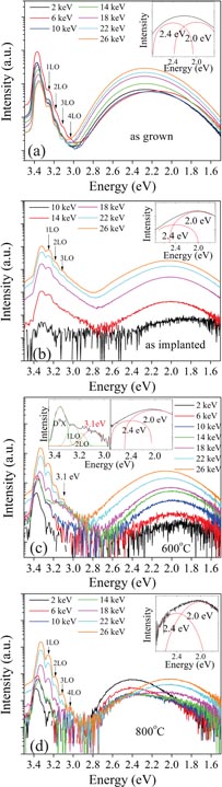
Figure 2. Depth-resolved CL spectra at 80 K for ZnO single crystals in (a) as grown, (b) implanted with 1 × 1017 cm−2 H− at 100 keV, (c) implanted and annealed at 600 °C and (d) implanted and annealed at 800 °C. Insets show emissions at 2.0, 2.4 and 3.1 eV as revealed by Gaussian-fitting.
Download figure:
Standard image High-resolution imageThe electron–hole pair excitation depth at each EB is simulated with the Monte Carlo code CASINO to correlate the CL emission with respect to the implantation profile. The electron–hole pair generation (primary electron energy loss) is not linear over its maximum excitation depth Um, but instead has a stretched Gaussian shape that peaks at ∼0.3 Um. Therefore, in the present work, a corrected excitation depth U0 that corresponds to the depth at which 70% of electron–hole pairs are generated is used instead. Figures 3 show the intensity of the NBE emission INBE and the integrated intensity of the DL emission ID with respect to U0. ID (2.0 eV) and ID (2.4 eV) are obtained by deconvoluting the DL emission into 2 Gaussian distributions that peak at 2.0 eV and 2.4 eV, respectively. A Gaussian distribution that peaks at 3.1 eV is also used to fit the anomalous broad band at ∼3.1 eV found in the 600 °C sample, with the NBE band, the 1LO and 2LO of the free excitons were included in the fitting process, as shown in the inset of figure 2(c). The emission that peaks at 2.0 eV, 2.4 eV and 3.1 eV will be hereafter referred to as red, green and violet emission, respectively.

Figure 3. ID(2.4 eV), INBE and ID(2.0 eV) for ZnO single crystals in (a) as grown, (b) implanted with 1 × 1017 cm−2 H− at 100 keV, (c) implanted and annealed at 600 °C and (d) implanted and annealed at 800 °C.
Download figure:
Standard image High-resolution imageAfter implantation, the sample shows very low DRCLS emission from the surface to U0 ≈ Rp as illustrated in figures 3(b), suggesting that the most defective layer in the implanted region is located at U0 < Rp. After annealing, the emission from this defective layer does not completely recover to the one in the as grown sample as shown in figure 3(a), and results in a plateau region with low INBE from the surface to U0 ≈ 500 nm. This suggests that the non-radiative recombination channels caused by the high dose H implantation are not completely annealed out even after 800 °C. Nonetheless, for the annealed samples, the DL emission does not appear to share the same depth profile trend as the NBE. For the red emission, ID (2.0 eV) is found to increase with higher EB, irrespective of the annealing temperature. For the 600 °C sample, there is also a small peak for ID (2.0 eV) at U0 ≈ 500 nm, showing a possible increase of the defect concentration related to red emission. On the other hand, for the green emission, ID (2.4 eV) appears to be completely suppressed after 600 °C annealing, which could be a result of the passivation of deep level defects by the implanted H. This is supported by the SIMS data in figure 1(b), where no H is detected at depth >1000 nm with ID (2.4 eV) increasing sharply. However, after 800 °C annealing, the green emission is significantly enhanced in the near surface region and becomes more intense than the red emission. For the violet emission that is only observable at EB ≈ 10–20 keV after 600 °C annealing, ID (3.1 eV) increases from low EB, then peaks at 14 keV/U0 ≈ 430 nm, and eventually decreases when DRCLS probes deeper into the sample. The ID (3.1 eV) peak is located at approximately the same depth as the small peak of ID (2.0 eV). This depth is also where the plateau region of near surface low INBE ends.
The surface enhancement of the green emission after 800 °C annealing has also been reported in electron irradiated melt-grown samples [25] and as-received hydrothermally grown samples [26]. This increase has been ascribed to either the dissociation of the non-radiative VO–acceptor defects complexes [25], or to the loss of H near the surface, as re-annealing the samples in forming gas (5% H2/95% N2 or 5% H2/95% Ar2) quenches the green emission [26]. Both of these studies propose that the passivated defects involved with the green emission could be due to Cu, which has often been assigned as a source for green emission, especially when fine structures resembling longitudinal optical (LO) phonon replicas with a periodic energy spacing of 72 meV is observed on the high energy slope of the band [27, 28]. As CuH and CuH2 complexes dissociate below 800 °C [29], which is the temperature where the green emission starts to re-appear, this may also explain the surface enhancement of the green emission after 800 °C annealing observed in the present work. Similar to the works by Allen et al [26] and Knutsen et al [25], in the PL spectrum that is collected at 14K for the 800°C sample as shown in figure 4, fine structures separated by ∼72 meV occur on the high energy slope of the DL emission. The SIMS measurement also shows an accumulation of Cu concentration (∼1 × 1018 cm−3) near the surface that decreases gradually to the background concentration (∼1 × 1015 cm−3) at a depth of ∼400 nm (see the online supporting information for the Cu concentration-depth profile measured by SIMS for the H implanted sample before and after implantation and annealing (stacks.iop.org/JPhysD/47/342001/mmedia)). Therefore, Cu may be one of the defects related to the green emission enhancement after 800 °C annealing, and is susceptible to passivation by H after 600 °C annealing.

Figure 4. 14 K PL spectra for ZnO single crystals implanted with 1 × 1017 cm−2 H− at 100 keV and annealed at 800 °C, showing phonon replicas that are periodically separated by ∼72 meV at the high energy side of the deep level band.
Download figure:
Standard image High-resolution image
The broad violet band centred at 3.1 eV that appears after 600 °C annealing (in figure 2(c)) is uncommon, but when observed it has been attributed to (a) a donor to acceptor pair (DAP) [30], (b) shallow donor levels such as Zni [31], and (c) LiZn acceptor states located at ∼0.3 eV above the valence band [32]. Figure 3(c) shows that the violet emission peaks at UO ≈ 500 nm, which is slightly shallower than the peak of the SIMS implanted H profiles at ∼600 nm in figure 1(b). As discussed previously, depth profiling with DRCLS cannot be extracted linearly with respect to EB. The actual depth for the violet emission peak may be slightly different than the one derived from the 70% of the maximum CL generation depth. In the implanted layer, it has been shown that the region shallower than Rp is mostly filled with vacancies, while the interstitial-rich region is located at a depth deeper than Rp [33]. As discussed previously, the small peak of the red emission at UO ≈ 500 nm in figure 3(c) appears to overlap with the depth at which the violet emission peaks. Despite still being controversial, the red emission is typically suggested to be related to the VZn and clusters thereof [20]. In addition, ID (3.1 eV) also has a depth profile that is similar in shape and trend to the SIMS Li profile in the 600 °C annealed sample in figure 1(b). This may indicate a correlation between the violet emission, vacancies and Li, in general agreement to the study by Zhang et al that relates the violet emission to LiZn [32]. However, other sources mentioned earlier for the violet band may also not be ruled out here, such as the DAP and free to bound recombination, which may have a weak phonon coupling that makes the phonon replicas hard to be detected.
4. Conclusions
In conclusion, the annealing temperature is found to influence the shape, size and empty volume density of voids formed in ZnO single crystals implanted with 1 × 1017 cm−2 H− ions. The voids change from a round to a faceted shape when the annealing temperature increases from 600 to 800 °C. DRCLS measurements also reveal a considerable difference in the depth dependence of the green, red and violet emissions after thermal annealing. The green emission is heavily quenched by H after 600 °C annealing, while loss of H near the sample surface results in a re-appearance and significant enhancement in the near surface region following 800 °C annealing. The violet emission that is only stable at <600 °C is found to be related to Li and vacancies.
Acknowledgments
Financial support from the Australian Research Council and the Research Council of Norway is acknowledged. We also thank the Australian National Fabrication Facility (ACT node) and the Centre for Advanced Microscopy (AMMRF node) for access to their facilities.