
Abstract
The relationship between thermal conductivity and microstructures of aluminium nitride films is reported. Films were deposited on silicon substrates by magnetron sputtering of a pure Al target in nitrogen argon plasma at low temperatures (<300 °C) with thickness ranging from 150 to 3500 nm. Balanced and unbalanced magnetron configurations were used for different nitrogen contents in the gas phase. Various microstructures were thus created and their thermal conductivity was measured with the transient hot strip technique. Depending on the crystalline structure of the films, the bulk thermal conductivity of the AlN films at room temperature varied between 2 and 170 W m−1 K−1. Unbalanced magnetron allowed achieving highly dense (0 0 2) oriented AlN films with a grain size in the 100 nm range, a low oxygen content close to 0.5 at% and a resulting bulk thermal conductivity as high as 170 W m−1 K−1. Such a crystalline quality resulted from the ion energy involved in the growth process. In contrast, balanced magnetron led to weakly textured AlN films containing 5 at% oxygen with a grain size in the 30 nm range and a resulting thermal conductivity ranging from 2 to 100 W m−1 K−1 depending on the microstructure. Otherwise, the thermal boundary resistance between AlN films deposited by unbalanced magnetron and the silicon substrate was found to be as low as 1.0 × 10⁻⁸ K m2 W−1. Such a value was in good agreement with the thickness of the interfacial amorphous layer determined in the 2 nm range by high resolution transmission electron microscopy.
Export citation and abstract BibTeX RIS
1. Introduction
Dielectric films are extensively used as electrical insulating and protective coatings in electronic circuits, electro-optical devices and optical systems. Their thermal conductivity is a key property of power devices, since it could substantially affect safety, reliability and performances. Nowadays, dielectric films most commonly used in circuits and devices are silicon dioxide, titanium dioxide and silicon nitride, which exhibit poor thermal conductivity. For instance, the thermal conductivity of amorphous silicon dioxide is around 1 W m−1 K−1. [1, 2]. For thermal management issues, there is an increasing need to replace such dielectrics with materials exhibiting higher thermal conductivity. In that respect, aluminium nitride (AlN) seems a good candidate. Thermal conductivity of single crystal AlN at room temperature has been reported equal to 320 W m−1 K−1 [3]. The high thermal conductivity and high dielectric constant of AlN are major factors favouring its use as a heat spreader material for electronic applications. For several decades, the thermal conductivity of bulk AlN has been extensively investigated [3–6]. Sintered polycrystalline AlN ceramics have thermal conductivity ranging from 17 to 285 W m−1 K−1 according to bulk defects or oxygen content [7, 8]. In addition, a high thermal conductivity is estimated to be about 320 W m−1 K−1 from some theoretical and experimental considerations [5]. Otherwise, high-quality AlN substrates with a thermal conductivity around 270 W m−1 K−1 are currently synthesized at high temperatures by CVD processes. Hence, it has been reported that the thermal conductivity of AlN can strongly decrease with increasing oxygen impurities content [3].
Generally, thermal conductivity of deposited thin films is different from their bulk form due to the special nature of the microstructure resulting from the growth process. The thermal conductivity can be affected by crystalline phases, crystallite sizes and structural imperfections such as impurities and lattice defects [3–7]. Thus, thermal conductivity values of amorphous and polycrystalline films can range over several decades depending on the defect density and oxygen content [8, 9]. Thermal conductivity of deposited thin films remains difficult to predict because microstructures are strongly impacted by the growth mechanisms and processing parameters [10, 11].
This paper reports on the microstructure dependence of the thermal conductivity of aluminium nitride thin films prepared by reactive magnetron sputtering. The films were deposited at low temperatures on silicon substrates with balanced and unbalanced magnetron configurations and different nitrogen contents in the gas phase. Various microstructures of AlN film were thus created and their thermal conductivity was determined with the transient hot strip technique. The relationship between the structural features of the films and their thermal conductivity was analysed.
2. Experimental details
2.1. Film preparation
AlN films were deposited on (1 0 0) silicon substrates by reactive dc magnetron sputtering of a pure aluminium target in an argon/nitrogen mixture. The deposition equipment consisted of a home-designed reactor equipped with a magnetron cathode and a 50 mm diameter aluminium target (99.9995% purity) supplied with a dc continuous voltage [12, 13], for deposition pressure in the 0.3–2 Pa range with a fixed total gas flux of 12.5 sccm and a nitrogen/argon ratio ranging from 10% to 60%. The power supply applied to the target was constant at 150 W. Deposition was carried out in planar configuration. Films were deposited without any intentional heating of the substrate. Nevertheless, during deposition, temperature increased up to around 270 °C due to plasma heating of the surface.
Two magnetic configurations of the magnetron cathode were used for promoting different types of film microstructure in deposited films while maintaining the same deposition chamber. In the first configuration, a balanced magnetron was involved and the distance between the target and the substrate was fixed at 30 mm. Such a configuration of the cathode provided a homogeneous discharge with low ion flux and electron density, involving a high flux of AlN reactive species and a low Al atom flux [12]. Thus, in that case, the deposition process enhanced the production of AlN dimers in the plasma phase and enabled us to synthesize AlN films (denoted b-AlN in the study) with different preferential orientations, namely (1 0 0, 0 0 2 and even 1 0 1), depending on the nitrogen content during deposition. In the second magnetic configuration, an unbalanced magnetron was used, and the distance between the target and the substrate was fixed at 40 mm. This configuration provided high fluxes of metallic species and ions, associated with a limited production of AlN species in the plasma phase and a strong increase in the ratio of ions to metal atom flux impacting the growing films [12]. In that case, the ion energy, provided by the ion flux to the growing film, was typically in the 20–30 eV range. Thus, dense (0 0 2) oriented AlN films (denoted u-AlN in the study) with high crystalline quality were obtained. Consequently, the energy transfer to the growing film was significantly increased with regards to a balanced magnetron configuration. The effect of such a process modification on the composition and structure of the synthesized films has been previously reported [12].
2.2. Thermal conductivity measurements
The thermal conductivity of AlN films was measured with the transient hot strip technique. A schematic of the experimental apparatus is presented in figure 1. The apparatus has been designed for testing films over a wide range of thermal conductivity and thickness. An aluminium strip of 20 µm×200 µm, used both as heater and electrical resistance thermometer, was patterned by photolithography of an Al film (20–60 nm thickness) deposited on each AlN film. Aluminium films were deposited at room temperature by dc magnetron sputtering of a pure aluminium target in argon plasma. This deposition technique was preferred to achieve a dense conductor with good adhesion and prevent diffusion of aluminium through the AlN films. Each test was carried out after incorporating the strip into a bridge (see figure 1). For tests, an input voltage U was applied across the bridge for 10 µs with a signal generator while the output voltage ΔV was detected over time with a digital oscilloscope through a 1 GHz differential probe (inset of figure 1). Then, the temperature rise of the strip ΔT was determined at any time with formula (1) given for a balanced bridge:

where β is the temperature coefficient of the strip. The thermal conductivity was determined by comparing thetime-dependent thermal impedance of the film/substrate system, expressed in °C W−1 according to relation (2):

where Z = ΔT/Q(Q is the heat generated by the strip), Ro denotes the electrical resistance of the strip, with numerical expressions (3a) and (3b) derived from a two-dimensional heat diffusion model of the film–substrate system, represented in figure 2. The thermal impedance Z in the Laplace transform domain is written as
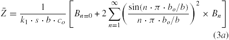
with
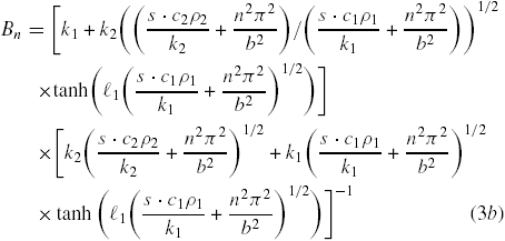
where k is the thermal conductivity, cρ the heat capacity, ℓ the thickness, s the Laplace variable and tanh stands for the hyperbolic tangent. Subscripts 1 and 2 refer to the film and to the substrate, respectively. Width and length of the strip are bo = 20 µm and co = 200 µm. The width of the substrate b is 1 mm. Z in the time-domain was obtained from (3a) and (3b) after real-space return with the Gaver–Stehfest algorithm [14]. The thermal conductivity of the film was treated as a free parameter fitted to minimize the differences between the model and the experimental signal. The fit was carried out by minimizing a least square function through the approach reported previously [15, 16]. The 2D model ((3a) and (3b)) supposed an isothermal strip with negligible thermal capacitance deposited on a homogeneous film with a constant thermal conductivity. Moreover, the substrate was taken as semi-infinite. Expressions (3a) and (3b) have been validated with three-dimensional finite element simulations. For tests, β was calibrated for each sample between 20 and 80 °C temperature. Depending on the aluminium thickness, Ro varied between 15 Ω and 35 Ω and β from 1.0 × 10⁻³ K−1 to 2.5 × 10⁻³ K−1. The thermal conductivity and heat capacity of the silicon substrate were 148 W m−1 K−1 and 1.6 × 10⁶ J m−3 K−1, respectively [17]. The measurement technique has been validated on different silicon oxide films and substrates (quartz, polycrystalline and single crystal Al2O3). For instance, a thermal conductivity of 1.3 W m−1 K−1 for a 500 nm thick SiO2 film was found, in good agreement with other data [1, 2]. In our experiments, the heat capacity of the AlN films was taken equal to 2.7 × 10⁶ J m−3 K−1 [17]. Figure 3 plots a representative thermal signal obtained on a 3.5 µm thick u-AlN film deposited on silicon, as the output voltage of the strip over time during 10 µs. In figure 3, the black line is the measured signal. The red signal is calculated with relations (3a) and (3b) after fitting the thermal conductivity of the film. In this case, the thermal conductivity was found equal to 130 ± 10 W m−1 K−1. The inset of figure 3 shows the relative difference between measured and calculated signals. The difference does not exceed 1%. However, it is worth noting that, for given parameters of the growth process, an intermediate layer was formed between the silicon substrate and the AlN film. The thickness of such an interfacial layer remains constant after the first stage of the deposition. Such a layer acts as a thermal barrier and is not considered in (3a) and (3b). Therefore, thermal conductivity k appears as a thickness-dependent property that can be related with the AlN thickness ℓ with relation (4) derived from a series-circuit relationship:

where RSi/AlN is the thermal boundary resistance due the amorphous layer between Si substrate and AlN film, and kb is the thermal conductivity in the bulk of the AlN film. Equation (4) is established for 1D steady-state conditions. This equation remained valid under our experimental conditions. First, since the strip size (20 µm×200 µm) was much larger than the films thickness, the heat diffusion in the film can be regarded as one-dimensional. In addition, during the experiments, the films act as pure resistance. Indeed, the time constants were very small (less than 300 ns) with regard to the time-window of the experiments (1–10 µs). Equation (4) was also confirmed by numerical simulations. However, because of the strip size, the effective conductivity measured from formulae (3a) and (3b), referred to the cross-plane conductivity, the in-plane conductivity not having any substantial effect.
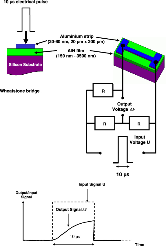
Figure 1. Schematic of the transient hot strip technique implemented for measuring the thermal conductivity of AlN films. An electrical pulse of 10 µs width was applied. Inset: input and output signal of the bridge within the strip is incorporated versus time.
Download figure:
Standard image
Figure 2. The two-dimensional heat diffusion model implemented for fitting the thermal conductivity of AlN films. k is the thermal conductivity, and cρ the heat capacity. Subscripts 1 and 2 refer to the AlN film and the silicon substrate, respectively. ℓ1 is the AlN film thickness.
Download figure:
Standard image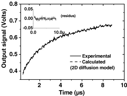
Figure 3. Output voltage of the bridge versus time measured with an aluminium strip deposited on 3,5 µm thick AlN film prepared with unbalanced magnetron sputtering on silicon substrate (1 0 0). Black line is the measured voltage as the dashed line is the signal calculated with relations (3a) and (3b). The inset shows the relative difference between the measured and the calculated signals.
Download figure:
Standard image2.3. Physical and chemical characterization
Scanning electron microscopy (SEM) imaging was performed with a JEOL JSM 6800 microscope equipped with an energy dispersive x-ray (EDX) spectrometer. For structural analysis, the x-ray diffraction (XRD) measurements were carried out with a Siemens D5000 x-ray diffractometer in Bragg–Brentano θ/2θ geometry using the Cu Kα radiation. The average grain size was determined with the Debye–Scherrer formula. Transmission electron microscopy (TEM) micrographs, used for analysing the Si–AlN interface, were recorded using a Hitachi HNAR9000 microscope. Crystalline quality was examined with Fourier-transform-infra-red analysis. The infrared absorption spectra (400–4000 cm−1) of the deposited films were recorded ex situ using a Nicolet 20 SXC spectrometer equipped with a HgCdTe (MCT) detector.
3. Results
XRD analysis revealed that AlN films were crystallized in pure wurtzite AlN phase with different preferential orientations depending on magnetic configurations (table 1). AlN films prepared with balanced magnetron (denoted hereafter b-AlN), with thickness ranging from 0.8 to 2.3 µm, were found poorly textured with a 5 at% oxygen content and a grain size in the 30 nm range. They had low density and several preferential crystalline orientations (1 0 0)/(0 0 2)/(1 0 1), depending on the nitrogen content in the gas phase. In contrast, the AlN films prepared with unbalanced magnetron (denoted hereafter u-AlN), with thickness ranging from 150 nm to 3.5 µm, had larger grain size in the 100 nm range and a lower oxygen content of 0.5 at%. They were dense and highly textured along (0 0 2). Their surface roughness (RMS), determined by atomic force microscopy (AFM), varied from 1 to 5 nm. Figure 4 shows representative SEM images of the section of both type of films deposited on silicon substrate. On the one hand, b-AlN films (figure 4(a)) have a columnar structure, typically obtained with magnetron sputtering techniques. On the other hand, the u-AlN films (figure 4(b)) are more compact, without visible voids between the weakly visible columns.
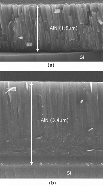
Figure 4. MEB images of transversal section of (a) 1.5 µm thick AlN film prepared with balanced magnetron sputtering on silicon substrate (1 0 0) and (b) 1.5 µm thick AlN film prepared with unbalanced magnetron sputtering on silicon substrate (1 0 0).
Download figure:
Standard imageTable 1. Main features of AlN films prepared with balanced and unbalanced magnetron sputtering (see [12] for details).
| Balanced magnetron b-AlN | Unbalanced magnetron u-AlN | |
|---|---|---|
| Crystalline orientation | N2 content dependent | c(0 0 2) oriented |
| Crystalline quality | Poorly textured | Good and highly textured |
| Oxygen content (% at.) | 5 | 0.5 |
| Average grain size (nm) | 20–30 | 100–150 |
| Internal stress | Tensile | Compressive |
| Internal stress (GPa) | 0.5 | −1.5 |
Thermal conductivities of b-AlN films and u-AlN films are given in the seventh column of table 2 for different film thicknesses and different nitrogen contents in the gas phase. The nitrogen content varied from 10% up to more than 30%. The films thicknesses were between 150 and 3500 nm (see table 2). The fourth and fifth columns of table 2 indicate the preferential crystalline orientation, determined by XRD, and the full width at half maximum (FWHM) of the FTIR (E1) T0 mode, respectively. The FWHM of the FTIR E1(T0) vibration mode is known to have significance for the crystalline quality of the films, as discussed later in that section. As evidenced in table 2, the thermal conductivity varies over several decades for b-AlN films and u-AlN films. Moreover, it is observed that the thermal conductivity of the u-AlN films is higher than b-AlN films for similar film thickness (see, for example, 100 W m−1 K−1 for the 1700 nm thick u-AlN films against 35 W m−1 K−1 for the b-AlN film of equivalent thickness). This fact was established for any nitrogen content (see the last columns of table 2). Overall, results were consistent with structural parameters derived from FTIR and XRD analysis: the thermal conductivity of u-AlN films, highly textured with 100 nm grain size and low oxygen content, was higher than the one of b-AlN films, which are poorly crystallized and weakly textured with an average 30 nm grain size and 5% oxygen content. Results confirmed that the thermal conductivity is strongly affected by phonon scattering and inclusion of oxygen atoms. As phonon mean-free path in AlN single crystal is in the order of 100 nm at room temperature [18], it was demonstrated that the conductivity should be more reduced for b-AlN (20 nm grain size, 5 at% oxygen) than u-AlN (100 nm grain size, 0.5 at% oxygen, see table 1).
Table 2. Effective and bulk thermal conductivity for AlN elaborated by unbalanced and balanced magnetron sputtering (respectively u-AlN and b-AlN), according to the crystalline orientation and crystalline quality as checked by the FWMH of the FTIR (E1) T0 mode. The main characteristics of AlN films are summarized in table 1.
| Magnetic configuration | AlN film thickness (nm) | Nitrogen content in the plasma phase (%) | Crystalline preferential orientation | FWHM of FTIR (E1) T0 mode (cm−1) | Crystalline quality | Oxygen content (at%) | Effective thermal conductivitya (W m−1 K−1) | Bulk thermal conductivityb (W m−1 K−1) |
|---|---|---|---|---|---|---|---|---|
| Balanced magnetic configuration b-AlN films | 2300 | <20 | (1 0 1) | 45 | Average | 5 | 15 | 68 |
| 2300 | (1 0 1) | 39 | 39 | 64 | ||||
| 2000 | (1 0 1) | 35 | Good | 44 | 98 | |||
| 1800 | (1 0 1) | 38 | 35 | 68 | ||||
| 1700 | 20–30 | (0 0 2) | 86 | Average | 5 | 4 | 4.2 | |
| 1600 | (0 0 2) | 56 | Average | 26 | 44 | |||
| 1000 | (0 0 2) | 91 | Poor | 14 | 22 | |||
| 1800 | >30 | (1 0 0) | 114 | Poor | 5 | 2.5 | 2.6 | |
| 1000 | (1 0 0) | 142 | Very poor | 6 | 7 | |||
| 800 | (1 0 0) | 162 | Very poor | 2.5 | 2.4 | |||
| Unbalanced magnetic configuration u-AlN films | Excellent | 0.5 | ||||||
| 150 | 20 | (0 0 2) | <30 | 17 ± 8 | 170 ± 30 | |||
| 800 | (0 0 2) | 40 ± 10 | 170 ± 30 | |||||
| 1700 | (0 0 2) | 100 ± 15 | 170 ± 30 | |||||
| 3500 | (0 0 2) | 130 ± 10 | 170 ± 30 |
aEffective thermal conductivity values are given with an accuracy of ±10%. bBulk thermal conductivity and the thermal boundary resistance were estimated from figure 5 and figure 7 and relation (4). The thermal boundary resistance for u-AlN films was found equal to 1 × 10⁻⁸ K m−2 W−1. For b-AlN films, the thermal boundary resistance was estimated to 2.5 × 10⁻⁸ K m−2 W−1, while considering proportional to the interfacial layer thickness.
According to structural parameters indicated in table 1, b-AlN films were weakly crystallized along a preferential orientation, depending on the nitrogen content in the gas phase during deposition. As displayed in table 2, thermal conductivities of b-AlN films ranged from 2 W m−1 K−1 to approximately 40 W m−1 K−1. The AlN films were mainly (1 0 1) oriented for low nitrogen content, lower than 20%, and (0 0 2) and (1 0 0) oriented for nitrogen content in the 20–30% range and above 30%, respectively. Thermal conductivity of (1 0 0) oriented films was lower than 10 W K−1 m−1, and varied in the range 4–26 W m−1 K−1 and 30–50 W m−1 K−1 for (0 0 2) and (1 0 1) oriented films, respectively. It was confirmed that the thermal conductivity in the range 30–50 W m−1 K−1 referred to the narrower FWHM, thus indicating higher crystalline quality. For all films, it was established that the wider the FWHM of the IR E1(T0) vibration mode, the lower the thermal conductivity. This fact is illustrated in figure 5 that plots the thermal conductivity of b-AlN films, as defined in relations (3a) and (3b), versus the FWHM of FTIR (E1) T0 vibration mode. As expected, figure 5 reveals a good correlation between the FWHM of the FTIR (E1) T0 vibration mode and the thermal conductivity with regard to the crystalline orientation of the films, namely (1 0 0), (0 0 2) and (1 0 1). Clearly, the curve of figure 5 shows three distinct domains for thermal conductivity and FWHM referring to the preferential crystalline orientation of materials. Moreover, figure 6 compares the FTIR spectra obtained for two b-AlN films (1 0 1) oriented having different thermal conductivity values of 44 and 15 W m−1 K−1. Figure 6 proves that, even if FWHM is quite similar, as shown in figure 5, their transmission spectra, and particularly the (E1) T0 vibration peak, should be more appropriate to gauge the crystalline quality. Transmitted intensity substantially increases with the thermal conductivity.

Figure 5. Thermal conductivity of AlN films of type (1) versus FWHM of FTIR E1 (T0) mode, which is significant for the crystalline quality of the films. Note that the effective thermal conductivity values are given with an accuracy of ± 10%.
Download figure:
Standard image
Figure 6. Comparison of FTIR spectra obtained for two AlN films exhibiting a thermal conductivity of 44 W m−1 K−1 (red line) and 15 W m−1 K−1 (black line).
Download figure:
Standard imageThermal conductivity of u-AlN films of 150 nm, 800 nm, 1700 nm and 3500 nm, prepared under the same experimental conditions, was found equal to 17 W m−1 K−1, 40 W m−1 K−1, 100 W m−1 K−1 and 130 W m−1 K−1, respectively. This result indicated that, due to growth process, the as-prepared materials are heterogeneous by nature, especially through the cross-plane direction. In other words, it was confirmed that the crystalline quality of u-AlN changed with thickness to a large extent. As already mentioned, the weak thermal conductivity of the amorphous interfacial layer, between the silicon substrate and the AlN film, has a major contribution, especially in the case of thinner films (see relation (4)). Figure 7 plots the thermal resistance of the u-AlN film, ℓ/k according to the thickness. The uncertainty on the interfacial thermal resistance was largely due to the uncertainty on the silicon parameters reported in the literature. Therefore, the linear fit associated with the experimental points of figure 7 stands as the most credible profile (i.e. thermal resistance versus thickness). Measurements (black squares) were found in good agreement with relation (4) (discontinuous black line). Therefore, the thermal boundary resistance of Si/AlN interface was found to be as low as 1 × 10⁻⁸ W−1 K m2. Thus, the uncertainty was estimated as equal to ±0.5 × 10 −8 K m2 W−1, according to measurements performed for the smaller resistance. The interfacial resistance was attributed to the 2 nm thick interfacial amorphous layer observed by high resolution TEM, as shown in figure 8(a). Note that it remains much lower than the one measured by Zhao et al for sputtered AlN films by the thermo-reflectance technique [19]. The bulk thermal conductivity of the u-AlN films was found to be as high as 170 ± 30 W m−1 K−1 by extraction from the slope in figure 6. This highlights the high bulk crystalline quality of the deposited u-AlN film.
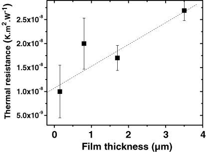
Figure 7. Thermal resistance of AlN films prepared with unbalanced magnetron sputtering versus thickness. The discontinuous line obtained by linear regression and according to relation (4), the bulk thermal conductivity and the boundary resistance are found to be equal to 170 W m−1 K−1 and 1 × 10⁻⁸ K m−2 W−1, respectively.
Download figure:
Standard image
Figure 8. (a) HRTEM image of the AlN/Si interface for an AlN film prepared by unbalanced magnetron sputtering (u-AlN). Thickness of the amorphous intermediate layer is 2 nm and the measured thermal boundary resistance is 1 × 10⁻⁸ K m−2 W−1. (b) HRTEM image of an AlN film prepared with balanced magnetron sputtering (b-AlN). Thickness of the amorphous intermediate layer is 5 nm. The thermal boundary resistance was estimated to be 2.5 × 10⁻⁸ K m−2 W−1, while considering the thermal resistance proportional to the interfacial layer thickness.
Download figure:
Standard imageMoreover, high resolution TEM observations revealed a 5 nm thick amorphous interface for b-AlN films (figure 8(b)). The interfacial thermal resistance was primarily originated from the amorphous layer given by TEM observation (figure 8), thickness of 2 nm and 5 nm for u-AlN and b-AlN films, respectively. Further, the thermal conductivity of the amorphous layer was considered as constant for all AlN samples. Then, the interfacial resistance should be proportional to the thickness of the amorphous layer. As HRTEM observations of b-AlN films (figure 8(b)) evidenced an amorphous layer thickness of 5 nm (i.e. 2.5 times thicker than the one of u-AlN films), the interfacial resistance was taken 2.5 times higher than the one of the u-AlN films. We thus reasonably assumed a thermal boundary resistance in the order of 2.5 × 10⁻⁸ K m2 W−1.
As checked on HRTEM images, no delamination of the films was observed. This fact was also confirmed by a previous study of our group [20] demonstrating that thick AlN films with a good crystalline quality and a predominant (0 0 2) texture can be deposited by dc reactive on silicon substrate without any delamination. For thick films, we observed that the improvement of the crystalline quality of the films is linked with a decrease in the compressive stress as a function of thickness. This effect is beneficial for the film adhesion.
Therefore, the bulk thermal conductivity of b-AlN films, reported in the last column of table 2, has been estimated by relation (4) from measured values given in the eight columns of table 2. Comparison between thermal conductivity of u-AlN and b-AlN in the bulk is analogous to the ones conducted above regarding apparent values (right part of table 2). Our study evidenced that higher thermal conductivity values are observed for AlN films with higher crystalline quality. High thermal conductivities were found for u-AlN films which were better crystallized, denser and highly textured along the (0 0 2) direction. In contrast, b-AlN films were characterized by low thermal conductivity related to their lower crystalline quality. Thermal conductivities of b-AlN films are comparable to the data reported in the literature for AlN thin films, i.e. in the 1–10 W m−1 K−1 range [11, 21]. To our knowledge, the high value of 170 W m−1 K−1 measured for u-AlN film is among the best ever reported for thin films. Such a value has been obtained thanks to an optimization of the crystalline quality of the AlN films, while controlling the deposition process parameters. The reached value is not so far from the value 272 W m−1 K−1, reported for bulk AlN substrates synthesized at high temperature in the 800–1000 °C range [22]. Finally, this study highlights the effective correlation between the thermal conductivity, crystalline quality and microstructure of AlN thin films deposited by reactive magnetron sputtering at low temperatures.
4. Conclusion
This study investigated the thermal conductivity of AlN films deposited by reactive magnetron sputtering at low temperatures (<300 °C). Deposition was performed by magnetron sputtering of a pure Al target in nitrogen argon plasma on silicon substrates with film thickness ranging from 150 to 3500 nm. We highlighted the effects of magnetron configurations, i.e. balanced and unbalanced, and nitrogen content in the gas phase on the thermal conductivity of AlN films. Various microstructures were thus created and their thermal conductivity was measured with the transient hot strip technique. We evidenced the relationship between thermal conductivity, crystalline quality and microstructures of aluminium nitride films. Depending on the crystalline structure of the films, the bulk thermal conductivity of the AlN films at room temperature varied in a wide range. Unbalanced magnetron achieved highly crystallized films with a bulk thermal conductivity as high as 170 W m−1 K−1 and low oxygen content close to 0.5 at%. Such a crystalline quality resulted from the high ion energy involved in the growth process. In contrast, balanced magnetron gave weakly crystallized films containing 5 at% oxygen and a thermal conductivity ranging from 2 to 100 W m−1 K−1 according to the microstructure. Otherwise, the thermal boundary resistance between AlN films deposited by unbalanced magnetron and the silicon substrate was found to be as low as 1.0 × 10⁻⁸ K m2 W−1. This resistance was attributed to the amorphous layer created between the AlN film and the Si substrate, as evidenced by high resolution TEM observations. The high thermal conductivity obtained for AlN, prepared with unbalanced magnetron sputtering, demonstrates the ability of magnetron reactive processes to offer a suitable route for synthesizing dielectric thin films with high thermal conductivity at temperatures compatible with the back end process of device fabrication.
Acknowledgments
This work has been financially supported by the Alcatel-Thales III-V Lab (Fr.). Professor Abdou Djouadi is deeply acknowledged for his early contribution in the study and fruitful discussions related to AlN film properties. Alain Barreau from the CMC-Université de Nantes (Fr.) is thanked for SEM observations.